
Influence of the Bias Voltage on Effective Electron Velocity in AlGaN/GaN High Electron Mobility Transistors
Abstract
:1. Introduction
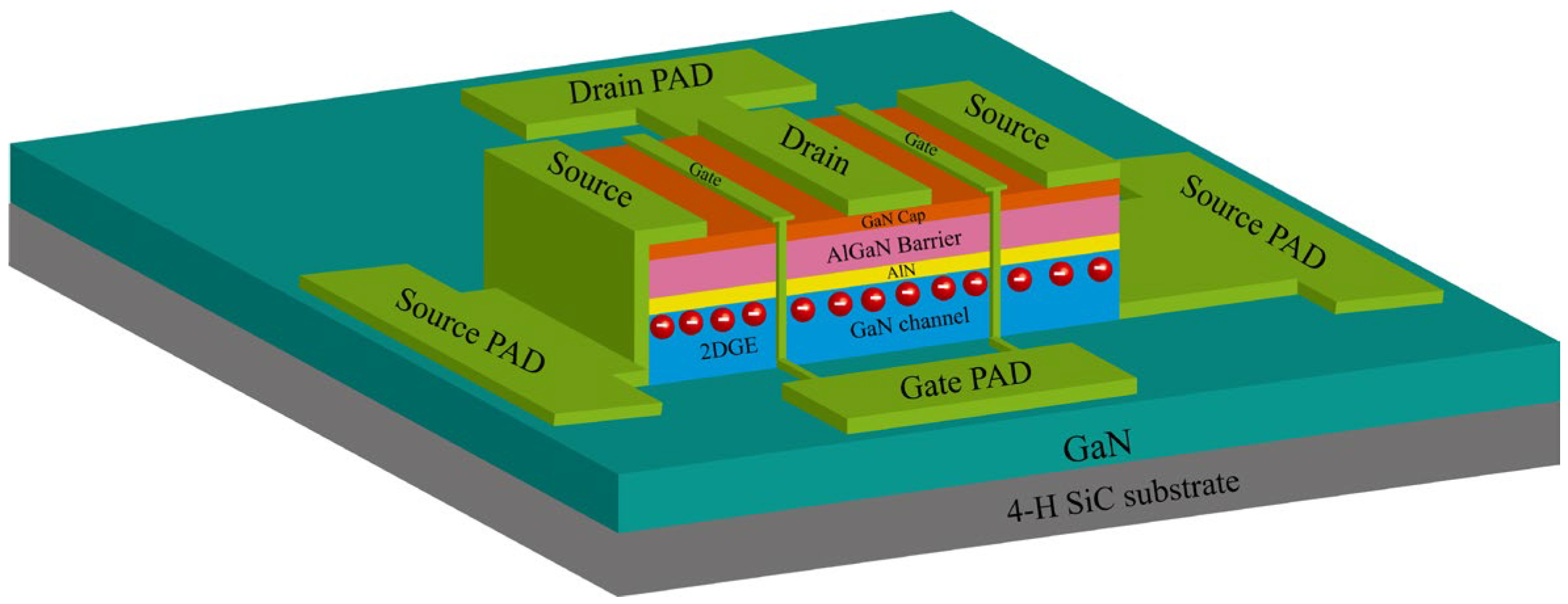
2. Experiments
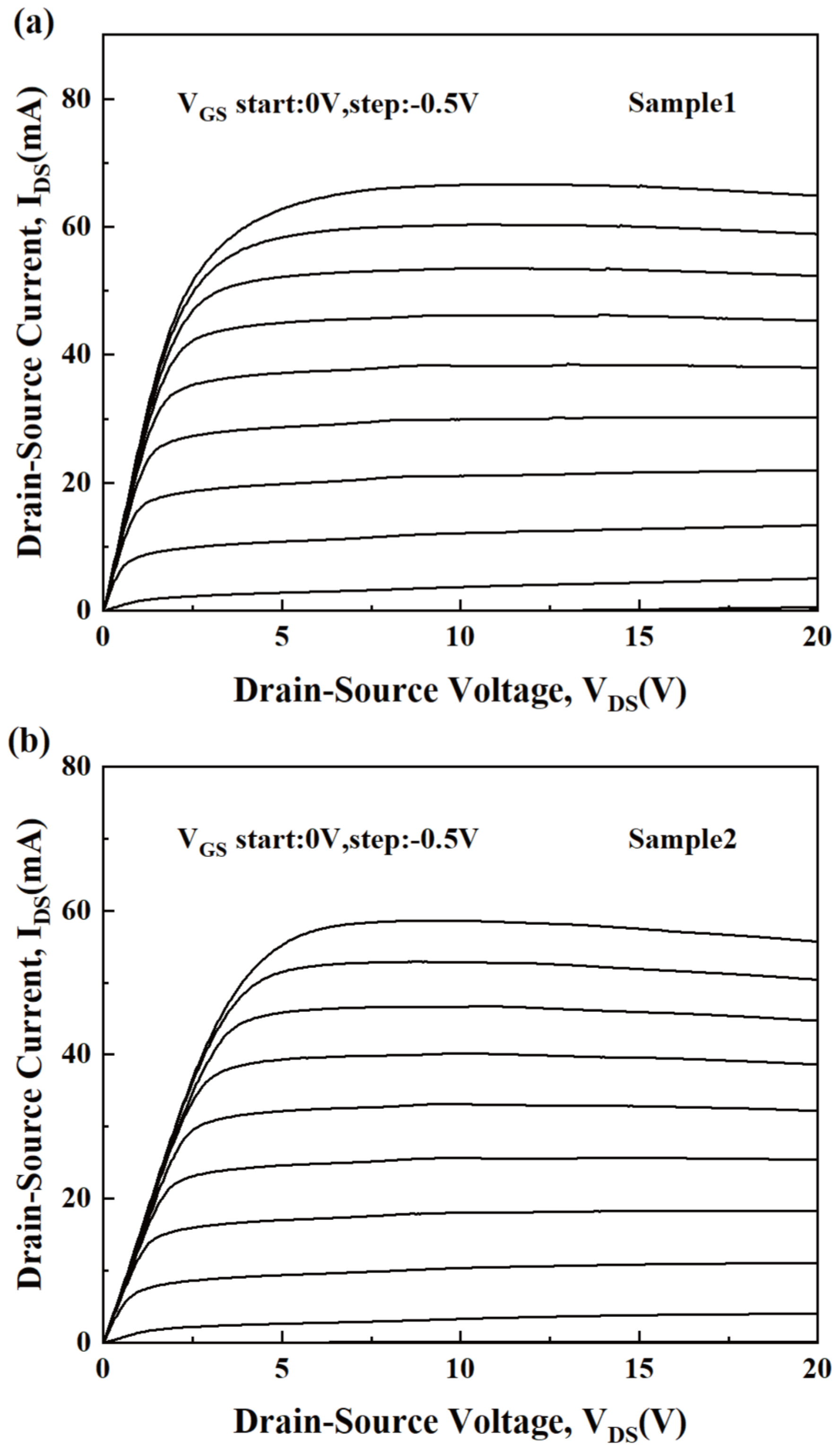
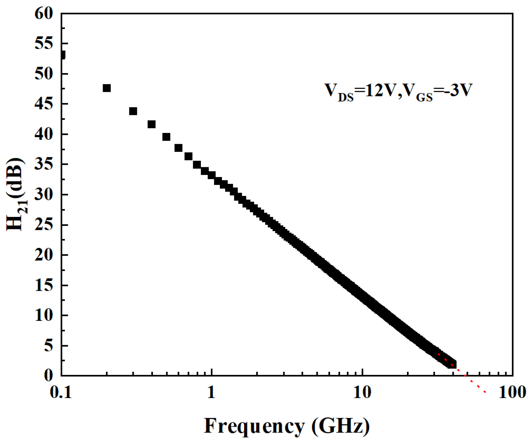
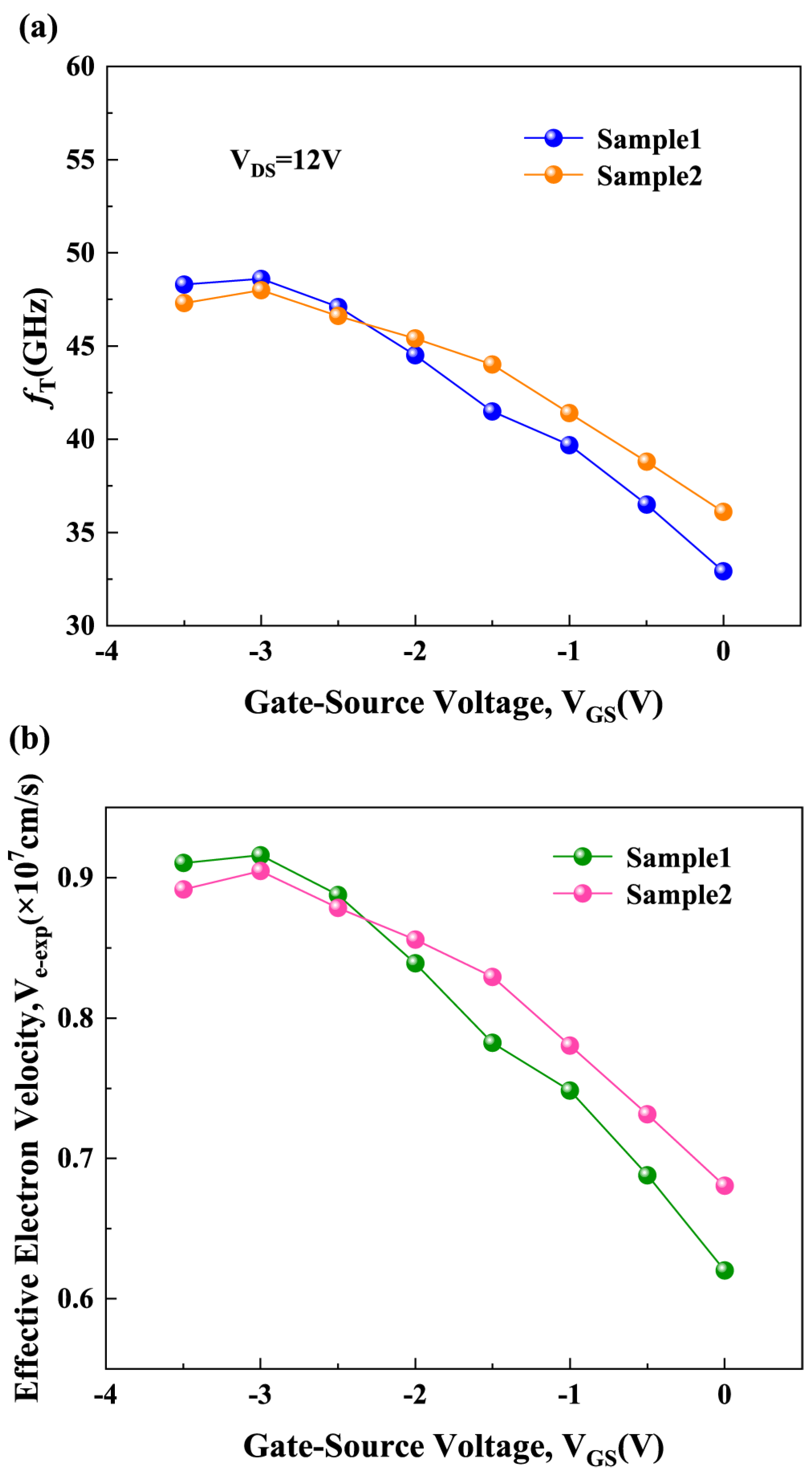
3. Results and Discussion
4. Conclusions
Author Contributions
Funding
Data Availability Statement
Conflicts of Interest
References
- Wang, Z.; Wang, G.; Liu, X.; Wang, S.; Wang, T.; Zhang, S.; Yu, J.; Zhao, G.; Zhang, L. Two-dimensional wide band-gap nitride semiconductor GaN and AlN materials: Properties, fabrication and applications. J. Mater. Chem. C 2021, 9, 17201–17232. [Google Scholar] [CrossRef]
- Akpınar, Ö.; Bilgili, A.K.; Öztürk, M.K.; Özçelik, S. Electron transport properties of Al0.3Ga0.7 N/GaN high electron mobility transistor (HEMT). Appl. Phys. A 2020, 126, 623. [Google Scholar] [CrossRef]
- Ajayan, J.; Nirmal, D.; Mohankumar, P.; Mounika, B.; Bhattachary, S.; Tayal, S.; Fletcher, A.S.A. Challenges in material processing and reliability issues in AlGaN/GaN HEMTs on silicon wafers for future RF power electronics & switching applications: A critical review. Mater. Sci. Semicond. Process. 2022, 151, 106982. [Google Scholar] [CrossRef]
- Wang, F.; Chen, W.; Wang, Z.; Wang, Y.; Lai, J.; Sun, R.; Zhou, Q.; Zhang, B. A low turn-on voltage AlGaN/GaN lateral field-effect rectifier compatible with p-GaN gate HEMT technology. Semicond. Sci. Technol. 2021, 36, 034004. [Google Scholar] [CrossRef]
- Han, Z.; Li, X.; Wang, H.; Liu, Y.; Yang, W.; Lv, Z.; Wang, M.; You, S.; Zhang, J.; Hao, Y. Highly Responsive Gate-Controlled p-GaN/AlGaN/GaN Ultraviolet Photodetectors with a High-Transmittance Indium Tin Oxide Gate. Micromachines 2024, 15, 156. [Google Scholar] [CrossRef]
- Moon, J.-S.; Wong, J.; Grabar, B.; Antcliffe, M.; Chen, P.; Arkun, E.; Khalaf, I.; Corrion, A.; Chappell, J.; Venkatesan, N.; et al. 360 GHz fMAX Graded-Channel AlGaN/GaN HEMTs for mmW Low-Noise Applications. IEEE Electron Device Lett. 2020, 41, 1173–1176. [Google Scholar] [CrossRef]
- Feng, C.; Jiang, Q.; Huang, S.; Wang, X.; Liu, X. Gate-Bias-Accelerated VTH Recovery on Schottky-Type p-GaN Gate AlGaN/GaN HEMTs. IEEE Trans. Electron Devices 2023, 70, 4591–4595. [Google Scholar] [CrossRef]
- Islam, N.; Mohamed, M.F.P.; Khan, M.F.A.J.; Falina, S.; Kawarada, H.; Syamsul, M. Reliability, Applications and Challenges of GaN HEMT Technology for Modern Power Devices: A Review. Crystals 2022, 12, 1581. [Google Scholar] [CrossRef]
- DiSanto, D.W.; Bolognesi, C.R. At-bias extraction of access parasitic resistances in AlGaN/GaN HEMTs: Impact on device linearity and channel electron velocity. IEEE Trans. Electron Devices 2006, 53, 2914–2919. [Google Scholar] [CrossRef]
- Zhou, Q.; Zhang, A.; Zhu, R.; Shi, Y.; Wang, Z.; Liu, L.; Chen, B.; Jin, Y.; Chen, W.; Zhang, B. Threshold voltage modulation by interface charge engineering for high performance normally-off GaN MOSFETs with high faulty turn-on immunity. In Proceedings of the 2016 28th International Symposium on Power Semiconductor Devices and ICs (ISPSD), Prague, Czech Republic, 12–16 June 2016. [Google Scholar]
- Pampori, A.U.H.; Ahsan, S.A.; Dangi, R.; Goyal, U.; Tomar, S.K.; Mishra, M.; Chauhan, Y.S. Modeling of Bias-Dependent Effective Velocity and Its Impact on Saturation Transconductance in AlGaN/GaN HEMTs. IEEE Trans. Electron Devices 2021, 68, 3302–3307. [Google Scholar] [CrossRef]
- Wang, M.; Lv, Y.; Zhou, H.; Cui, P.; Liu, C.; Lin, Z. Bias-Dependent Electron Velocity Extracted From AlGaN/GaN HFETs and Its Impact on gm and fT. IEEE Electron Device Lett. 2024, 45, 160–163. [Google Scholar] [CrossRef]
- Chung, J.W.; Zhao, X.; Wu, Y.R.; Singh, J.; Palacios, T. Effect of image charges in the drain delay of AlGaN/GaN high electron mobility transistors. Appl. Phys. Lett. 2008, 92, 093502. [Google Scholar] [CrossRef]
- Romanczyk, B.; Guidry, M.; Zheng, X.; Li, H.; Ahmadi, E.; Keller, S.; Mishra, U.K. Bias-Dependent Electron Velocity Extracted From N-Polar GaN Deep Recess HEMTs. IEEE Trans. Electron Devices 2020, 67, 1542–1546. [Google Scholar] [CrossRef]
- Yang, M.; Lin, Z.; Zhao, J.; Cui, P.; Fu, C.; Lv, Y.; Feng, Z. Effect of Polarization Coulomb Field Scattering on Parasitic Source Access Resistance and Extrinsic Transconductance in AlGaN/GaN Heterostructure FETs. IEEE Trans. Electron Devices 2016, 63, 1471–1477. [Google Scholar] [CrossRef]
- Yang, M.; Lv, Y.; Feng, Z.; Lin, W.; Cui, P.; Liu, Y.; Fu, C.; Lin, Z. Study of source access resistance at direct current quiescent points for AlGaN/GaN heterostructure field-effect transistors. J. Appl. Phys. 2016, 119, 224501. [Google Scholar] [CrossRef]
- Cui, P.; Liu, H.; Lin, W.; Lin, Z.; Cheng, A.; Yang, M.; Liu, Y.; Fu, C.; Lv, Y.; Luan, C. Influence of Different Gate Biases and Gate Lengths on Parasitic Source Access Resistance in AlGaN/GaN Heterostructure FETs. IEEE Trans. Electron Devices 2017, 64, 1038–1044. [Google Scholar] [CrossRef]
- Cui, P.; Lv, Y.; Lin, Z.; Fu, C.; Liu, Y. Effect of polarization Coulomb field scattering on device linearity in AlGaN/GaN heterostructure field-effect transistors. J. Appl. Phys. 2017, 122, 124508. [Google Scholar] [CrossRef]
- Cui, P.; Lv, Y.; Liu, H.; Cheng, A.; Fu, C.; Lin, Z. Improved Linearity with Polarization Coulomb Field Scattering in AlGaN/GaN Heterostructure Field-Effect Transistors. Sci. Rep. 2018, 8, 983. [Google Scholar] [CrossRef]
- Cui, P.; Lv, Y.; Liu, H.; Cheng, A.; Luan, C.; Zhou, Y.; Lin, Z. Effect of different gate lengths on device linearity in AlGaN/GaN high electron mobility transistors. Phys. E Low-Dimens. Syst. Nanostruct. 2020, 119, 114027. [Google Scholar] [CrossRef]
- Haupt, C.; Maroldt, S.; Quay, R.; Pletschen, W.; Leuther, A.; Ambacher, O. Development of a high transconductance GaN MMIC technology for millimeter wave applications. Phys. Status Solidi (C)—Curr. Top. Solid State Phys. 2011, 8, 297–299. [Google Scholar] [CrossRef]
- Liu, Z.H.; Ng, G.I.; Arulkumaran, S.; Maung, Y.K.T.; Teo, K.L.; Foo, S.C.; Sahmuganathan, V. Comprehensive Study on the Bias-Dependent Equivalent-Circuit Elements Affected by PECVD SiN Passivation in AlGaN/GaN HEMTs. IEEE Trans. Electron Devices 2011, 58, 473–479. [Google Scholar] [CrossRef]
- Bouzid-Driad, S.; Maher, H.; Defrance, N.; Hoel, V.; De Jaeger, J.C.; Renvoise, M.; Frijlink, P. AlGaN/GaN HEMTs on Silicon Substrate With 206-GHz FMAX. IEEE Electron Device Lett. 2013, 34, 36–38. [Google Scholar] [CrossRef]
- Alim, M.A.; Rezazadeh, A.A.; Gaquiere, C. Thermal characterization of DC and small-signal parameters of 150 nm and 250 nm gate-length AlGaN/GaN HEMTs grown on a SiC substrate. Semicond. Sci. Technol. 2015, 30, 125005. [Google Scholar] [CrossRef]
- Jessen, G.H.; Fitch, R.C.; Gillespie, J.K.; Via, G.; Crespo, A.; Langley, D.; Denninghoff, D.J.; Trejo, M.; Heller, E.R. Short-Channel Effect Limitations on High-Frequency Operation of AlGaN/GaN HEMTs for T-Gate Devices. IEEE Trans. Electron Devices 2007, 54, 2589–2597. [Google Scholar] [CrossRef]
- Tasker, P.J.; Hughes, B. Importance of source and drain resistance to the maximum fT of millimeter-wave MODFETs. IEEE Electron Device Lett. 1989, 10, 291. [Google Scholar] [CrossRef]
- Manohar, S.; Pham, A.; Evers, N. Direct determination of the bias-dependent series parasitic elements in SiC MESFETs. IEEE Trans. Microw. Theory Tech. 2003, 51, 597–600. [Google Scholar] [CrossRef]
- Stiglitz, M.; Blanchard, C. MMIC Design: GaAs FETs and HEMTs; Artech House Inc.: Norwood, MA, USA, 1989. [Google Scholar]
- Campbell, C.F.; Brown, S.A. An analytic method to determine GaAs FET parasitic Inductances and drain resistance under active bias conditions. IEEE Trans. Microw. Theory Tech. 2001, 49, 1241–1247. [Google Scholar] [CrossRef]
- Lin, H.K.; Huang, F.H.; Yu, H.L. DC and RF characterization of AlGaN/GaN HEMTs with different gate recess depths. Solid-State Electron. 2010, 54, 582–585. [Google Scholar] [CrossRef]
- Jiang, G.; Fu, C.; Liu, Y.; Yang, G.; Cui, P.; Zhang, G.; Lv, Y.; Lin, Z. A novel method to determine bias-dependent source and drain parasitic series resistances in AlGaN/GaN high electron mobility transistors. Solid-State Electron. 2024, 220, 108991. [Google Scholar] [CrossRef]
- Wang, M.; Lv, Y.; Zhou, H.; Wen, Z.; Cui, P.; Liu, C.; Lin, Z. A Hybrid Simulation Technique to Investigate Bias-Dependent Electron Transport and Self-Heating in AlGaN/GaN HFETs. IEEE Trans. Electron Devices 2023, 70, 5479–5483. [Google Scholar] [CrossRef]
- Fang, T.; Wang, R.; Xing, H.; Rajan, S.; Jena, D. Effect of Optical Phonon Scattering on the Performance of GaN Transistors. IEEE Electron Device Lett. 2012, 33, 709–711. [Google Scholar] [CrossRef]
- Bajaj, S.; Shoron, O.F.; Park, P.S.; Krishnamoorthy, S.; Akyol, F.; Hung, T.-H.; Reza, S.; Chumbes, E.M.; Khurgin, J.; Rajan, S. Density-dependent electron transport and precise modeling of GaN high electron mobility transistors. Appl. Phys. Lett. 2015, 107, 153504. [Google Scholar] [CrossRef]
- Gurusinghe, M.N.; Davidsson, S.K.; Andersson, T.G. Two-dimensional electron mobility limitation mechanisms in AlxGa1-xN/GaN heterostructures. Phys. Rev. B 2005, 72, 045316. [Google Scholar] [CrossRef]
- Cserveny, S. Relationship between measured and Intrinsic conductances of MOSFETs. IEEE Trans. Electron Devices 1990, 37, 2413–2414. [Google Scholar] [CrossRef]
- Jiang, G.; Lv, Y.; Lin, Z.; Yang, Y.; Liu, Y.; Guo, S.; Zhou, Y. Polarization Coulomb field scattering with the electron systems in AlGaN/GaN heterostructure field-effect transistors. AIP Adv. 2020, 10, 075212. [Google Scholar] [CrossRef]
Disclaimer/Publisher’s Note: The statements, opinions and data contained in all publications are solely those of the individual author(s) and contributor(s) and not of MDPI and/or the editor(s). MDPI and/or the editor(s) disclaim responsibility for any injury to people or property resulting from any ideas, methods, instructions or products referred to in the content. |
© 2024 by the authors. Licensee MDPI, Basel, Switzerland. This article is an open access article distributed under the terms and conditions of the Creative Commons Attribution (CC BY) license (https://creativecommons.org/licenses/by/4.0/).
Share and Cite
Jiang, G.; Cui, P.; Fu, C.; Lv, Y.; Yang, M.; Cheng, Q.; Liu, Y.; Zhang, G. Influence of the Bias Voltage on Effective Electron Velocity in AlGaN/GaN High Electron Mobility Transistors. Micromachines 2024, 15, 1148. https://doi.org/10.3390/mi15091148
Jiang G, Cui P, Fu C, Lv Y, Yang M, Cheng Q, Liu Y, Zhang G. Influence of the Bias Voltage on Effective Electron Velocity in AlGaN/GaN High Electron Mobility Transistors. Micromachines. 2024; 15(9):1148. https://doi.org/10.3390/mi15091148
Chicago/Turabian StyleJiang, Guangyuan, Peng Cui, Chen Fu, Yuanjie Lv, Ming Yang, Qianding Cheng, Yang Liu, and Guangyuan Zhang. 2024. "Influence of the Bias Voltage on Effective Electron Velocity in AlGaN/GaN High Electron Mobility Transistors" Micromachines 15, no. 9: 1148. https://doi.org/10.3390/mi15091148