Article

Novel Bidirectional ESD Circuit for GaN HEMT

by
Pengfei Zhang
1,
Cheng Yang
1,
Jingyu Shen
2,
Xiaorong Luo
1,3,*,
Gaoqiang Deng
1,*,
Shuxiang Sun
1,
Yuxi Wei
1 and
Jie Wei
1
1
School of Integrated Circuit Science and Engineering, University of Electronic Science and Technology of China, Chengdu 610054, China
2
China Resources Microelectronics (Chongqing) Limited, Chongqing 401331, China
3
College of Microelectronics, Chengdu University of Information Technology, Chengdu 610225, China
*
Authors to whom correspondence should be addressed.
Micromachines 2025, 16(2), 129; https://doi.org/10.3390/mi16020129
Submission received: 11 November 2024 / Revised: 14 January 2025 / Accepted: 22 January 2025 / Published: 23 January 2025
(This article belongs to the Special Issue RF and Power Electronic Devices and Applications)

Abstract

:
In this paper, the ESD protection circuit for p-GaN gate HEMTs with bidirectional clamp is proposed and investigated. ESD clamp circuits consist of several forward diodes in serials and a reverse diode. During the ESD pulse, a discharging channel in the proposed ESD clamp is built and the gate to source voltage for p-GaN HEMTs is clamped at safety value. Based on the experimental verification, the proposed ESD clamps have bidirectional protection functionality by being triggered by a required voltage and exhibit a high secondary breakdown current in both forward and reverse transient ESD events. Meanwhile, the proposed ESD clamp circuit can decrease the power loss in a static state.
Keywords:
ESD; GaN; diode; p-GaN HEMT

1. Introduction

With superior working properties, the p-GaN gate high-electron mobility transistor (HEMT) has emerged as a prominent power device market. Meanwhile, its gate structure can be easily damaged by electrostatic discharge (ESD) events [1,2,3,4]. Recently, some articles have reported the ESD robustness of GaN HEMTs [5,6,7,8]. The commercial p-GaN gate HEMTs need to reach an industrial standard of more than 2 kV human body model (HBM) failure voltage (VHBM), which is equal to human body 1.5 kΩ, multiplied by secondary breakdown current (IS) (≥1.34 A) [9]. Therefore, incorporating ESD protection devices or circuits into GaN power systems has become a practical choice. Nevertheless, the p-GaN gate HEMTs equivalent VHBM for the gate-to-source condition is only 0.2∼0.33 kV [10]. Consequently, it is necessary to improve its gate-to-source ESD robustness by ESD circuit. Furthermore, since the protected HEMT also faces the threat of reverse electrostatic discharging current [11], reverse discharging properties should be taken into consideration during ESD protection circuit design.
However, there are only a few reports on ESD-protected circuit design for GaN HEMTs. An integrated GaN-based ESD protection structure is proposed by diodes in serials [12]. Nevertheless, the circuit limits to a unidirectional protection functionality and occupies a substantial chip area. Zener diode [13] has bidirectional clamp capability, but it is still incompatible with existing p-GaN HEMT technology. The resistive ESD protection circuit has bidirectional protection functionality [14], but the resistance value becomes important, referring to the trade-off between chip area and leakage current. The ESD additional power dissipation significantly impacts the overall performance and energy efficiency of the system, which is a crucial design concern. In addition, the combination of diodes with resistors can achieve high performance [15,16]. They also face a similar dilemma as resistive ESD protection circuits. As for capacitor ESD protection circuits [17,18,19], on the one hand, those circuits have relatively low leakage current, and, on the other hand, those circuits involving stray parameters during the transient situation lead to a small design margin. ESD circuits in recent fully integrated GaN designs [20,21] have more than one discharging device. Those clamps increase discharging resistance and require high device consistency.
In this work, we proposed novel self-triggered ESD discharging circuits, which consist of diodes, a current-limiting resistor and a p-GaN HEMT. The proposed ESD clamps can protect bidirectional ESD conditions and satisfy the industrial standard of bidirectional ESD robustness requirements. This work is organized as follows. Firstly, the structures and mechanisms of two ESD circuits are presented. Subsequently, the characteristics of the proposed ESD clamps are investigated. Finally, the impact of the proposed ESD circuit on the switching characteristics of p-GaN HEMTs is given.

2. Structure and Mechanism

Two bidirectional ESD circuits are proposed in this work. Compared to the resistive ESD clamp circuit, the low leakage current can be realized by incorporating a reverse diode into ESD clamps. Figure 1a gives the schematic ESD configuration (designated as clamp1). It consists of several diodes and a p-GaN HEMT. Multiple forward diodes are connected in series between the gate and drain of the HEMT, while a reverse diode is connected between the gate and source. Figure 1c,d show the second proposed topology (designated as clamp2). All the devices in the proposed ESD circuits could be readily integrated into p-GaN technology, making ESD design more convenient. Meanwhile, the gate-source shorted p-GaN HEMT may also be used as the diodes of clamp2. Given that conducting the experiment is more economical, equivalent circuit topology is printed on a circuit board (PCB) to verify the feasibility of circuit topology. Figure 1b,d are, respectively, clamp1’s and clamp2’s PCB layout and PCB picture. In clamp2, several forward diodes with one reverse diode are connected in series between the gate and drain and a current-limiting resistor is parallelly connected between the HEMT’s gate and the source.
When the Input node in Figure 1 meets a forward pulse of an ESD event under dynamic conditions, the forward current flows through the forward diodes, reverse diode or R2. Then, a transient voltage is built at the G node. Since the Input node obtains an increasing current from the ESD pulse, the voltage of the G node rises over the threshold voltage (Vth) of HEMT in the ESD clamp. It triggers the HEMT to turn on. Consequently, the forward electrostatic discharging current can flow through the ESD circuit, effectively clamping the gate-to-source voltage of the main protected HEMT within a safe operational range. The main protected HEMT is mainly at a steady state during its operating lifetime, and thus, the static condition of ESD protection circuits should also be taken into consideration.
The forward diode has an equivalent resistance (ron), and the reverse diode shows dynamic equivalent resistance (roff). The reverse diode’s static equivalent resistance approaches infinity (∞) as its parasitic capacitor has been fully charged. Therefore, Equations (1) and (2) show the proportional relationship between VTri and Vth of clamp1. As shown in Equations (3) and (4), the VTri is different between transient state and static state for clamp2. Generally, the forward triggering voltage should be larger than the gate operating voltage of 5 V of the protected HEMT in order not to disturb normal operation [22]. For p-GaN gate HEMT, its gate bias allowed for long-term reliable operation is approximately 8V [23]. The optimal VTri is between 5 V and 8 V. Equation (2) indicates that clamp1 clamps the gate of protected HEMT around Vth under static conditions regardless of the number of diodes, which cannot realize ESD protection. Nevertheless, Equations (3) and (4) theoretically verified the feasibility of clamp2.
c l a m p 1 (1) Transient : V T r i   V t h × ( 1 + n r o n r o f f ) (2) Static : V T r i   V t h × + n r o n   V t h
clamp 2 (3) Transient : V Tri     V th × 1 + r off + n 1 r on R 2 (4) Static : V Tri   V th × + n 1 r on + R 2 R 2  
To experimentally validate the proposed design at a low cost, an equivalent structure has been constructed on PCB. The diodes (RS1A) with ron around 44 mΩ and the commercial p-GaN HEMTs (INN700D240B) with Vth around 1.7 V are used in PCB test experiments. The transient ESD events are simulated by the transmission line pulsing (TLP) measurement system HED-T5000 (HANWA, Tokyo, Japan) and the TLP pulses are configured to have a duration of 100 ns and a rise time of 10 ns time referring to previous ESD studies [24]. Furthermore, the bidirectional TLP current–voltage (IV) characteristics of the proposed ESD clamps are extracted. Meanwhile, its bidirectional static IV characteristics are also extracted.

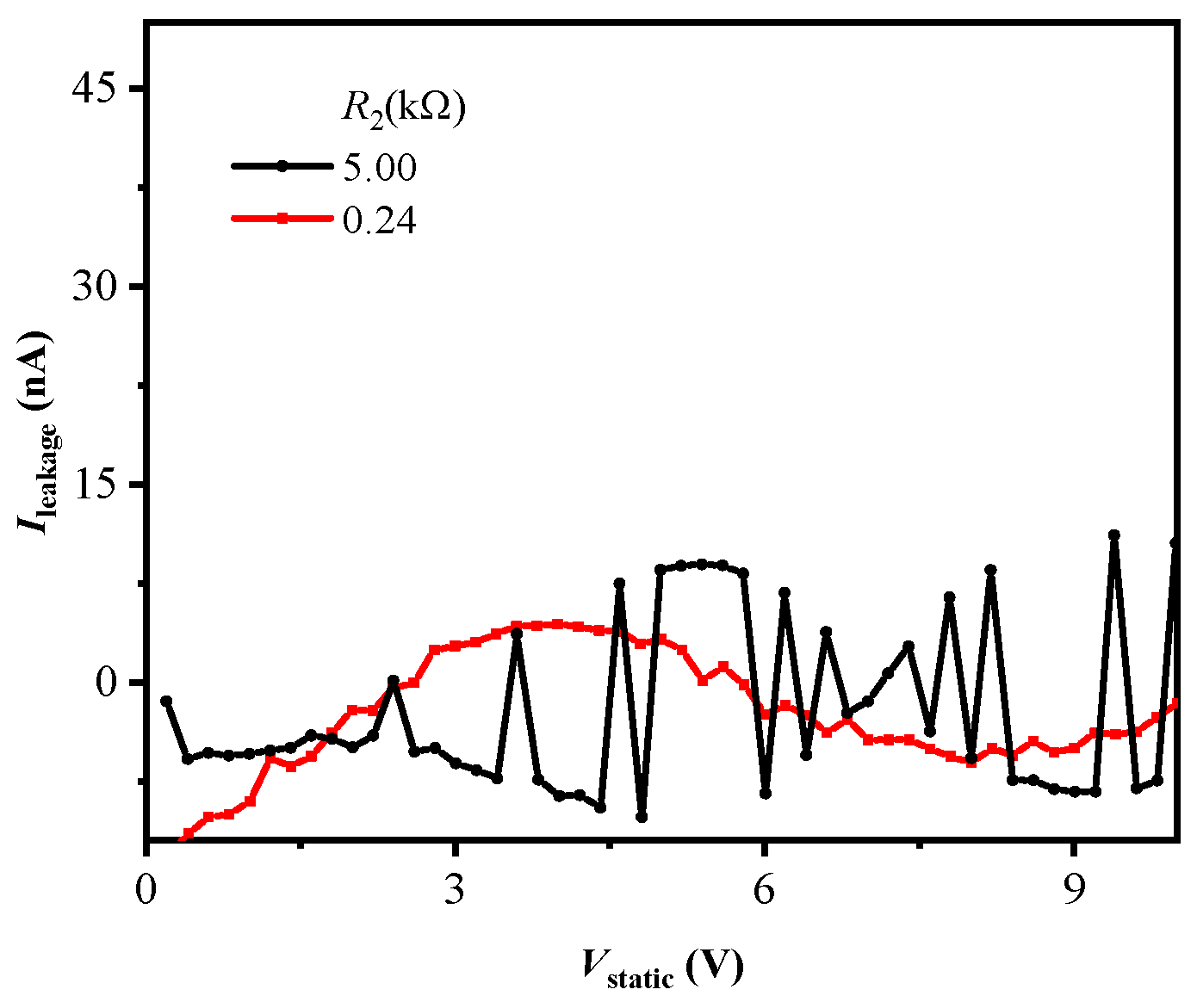
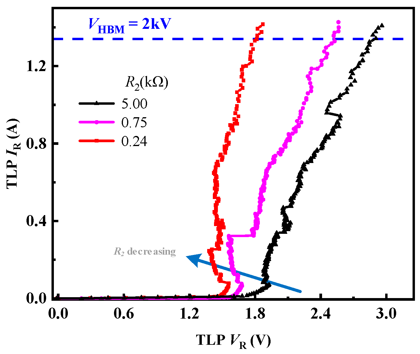
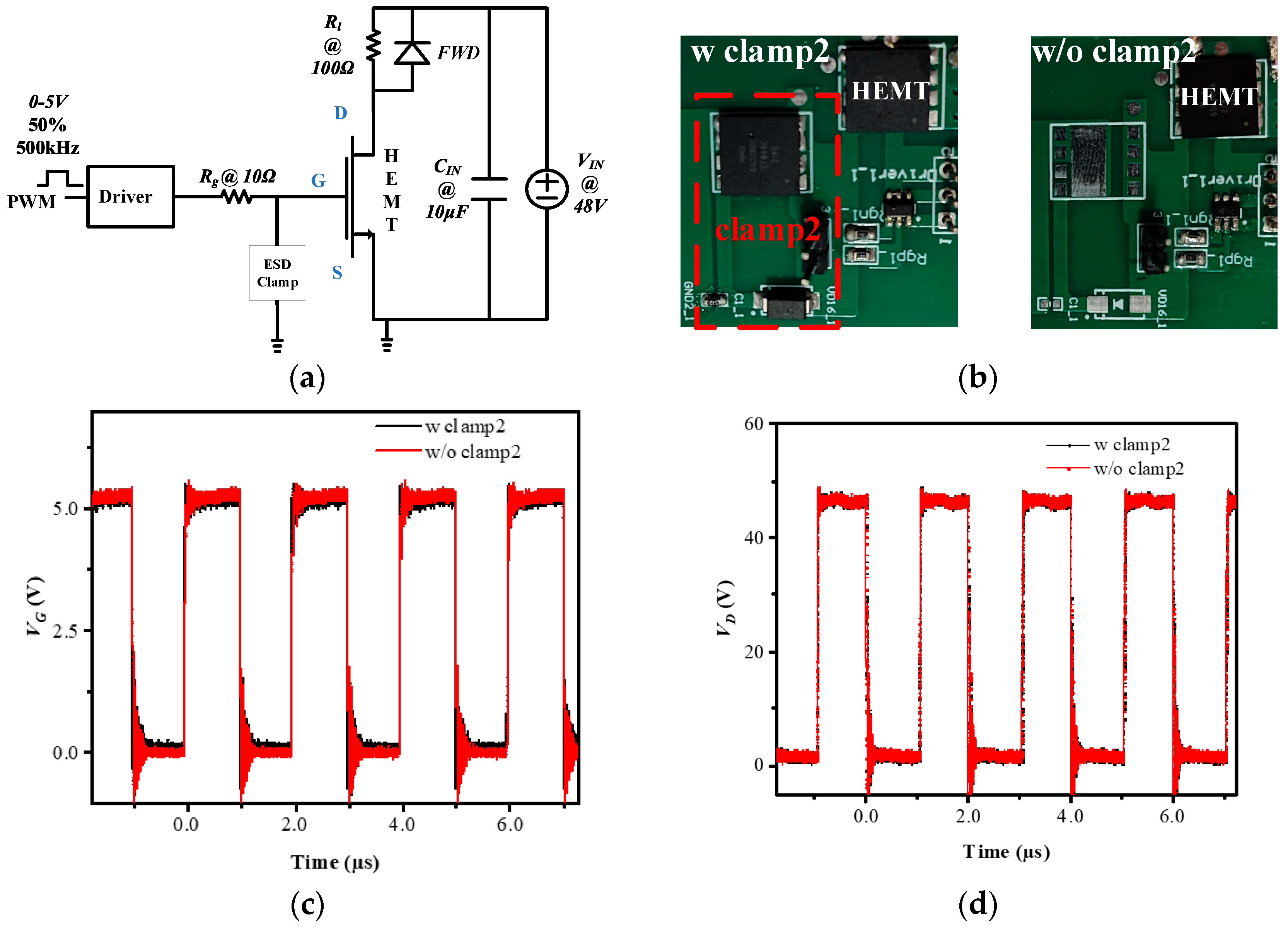
3. Results and Discussion

Figure 2a shows the TLP IV curves of clamp1 with a different number of forward diodes. During the ESD charges zapping at the Input node, clamp1 with 8 and 1 forward diodes could be triggered at 4.7 V and 1.8 V, respectively. It verifies that VTri positively correlated to the number of diodes. In addition, the two circuits both possessed a high secondary breakdown current of more than 1.34 A. It demonstrates that clamp1 could effectively release the accumulated electrostatic charges with the appropriate number of forward diodes. Nevertheless, the static I–V curves in Figure 2b show unacceptable low static VTri (lower than the gate operating voltage 5 V), and thus clamp1 cannot protect the main HEMT. By the way, static VTri decreases with the number of forward diodes. This could be explained by that the input static signal of the test machine may not filter out all the alternating signals.
Figure 3a shows that clamp2 can achieve more than 2 kV HBM failure voltage in a positive TLP test. With the increasing R2, VTri decreases from 17.7 V to 6 V and its decrease trend is decelerating in Figure 3b,c. Moreover, the curves in Figure 3a have an increasing slope when R2 rises, indicating an enhanced discharging efficiency. Given the ESD clamp design safety margin, a desirable R2 value should be chosen from 1 kΩ to 5 kΩ under the condition of 5 V ≤ VTri ≤ 8 V. As illustrated in Figure 3d, the number of forward diodes has little impact on the discharge characteristics because ron (~mΩ) is several orders of magnitude smaller than R2 (~kΩ).
Figure 4 gives the static leakage current of clamp2 with different values of R2. Clamp2 keeps leakage current at nano-ampere (nA) order, which proves static equivalent resistance of the reverse diode is also far larger than roff, as shown in Equation (4). Meanwhile, compared to resistive ESD clamp with milliampere (mA) leakage current [14], clamp2 decreases additional power dissipation.
Figure 5 compares the positive TLP I–V and positive leakage current characteristics with a resistive ESD circuit, clamp2 with RS1A and clamp2 with gate-source shorted p-GaN HEMT. (Since forward diodes of clamp2 have little impact on the circuit characteristics, the forward diodes or equivalent diodes of clamp2 are removed.) The clamp2 with RS1A and clamp2 with gate-source shorted p-GaN HEMT have the same R2 (5 kΩ) at the bias circuit. The conventional resistive ESD circuit has R1 (2 kΩ) and R2 (6 kΩ) at the bias circuit. All three ESD circuits show more than 1.34 A discharging property under the TLP test. Nevertheless, when it comes to static leakage property, two types of clamp2 reduce by more than five orders of magnitude. It proves that clamp2 design for ESD circuits can significantly reduce additional power dissipation.
We also investigate reverse TLP I–V characteristics of clamp2. Its reverse TLP I–V characteristics depend on R2. Its reverse VTri is evaluated in Equation (5).
Reverse   TLP :   V Tri     V th × 1 + R 2 r off + n 1 r on
Decreasing R2 leads to diminishing VTri, which is opposite to forward TLP I–V characteristics. Since the protected HEMT does not operate on reverse bias conditions, the reverse safety margin of the ESD clamp is 0 V to 8 V. Figure 6 shows that the clamp2 could be triggered by low voltage and achieve an IS more than 1.34 A under reverse TLP condition. It reveals that R2 is higher than roff. Meanwhile, reverse VTri fully locates at the safety margin when R2 changes from 0.24 kΩ to 5.0 kΩ. A desirable R2 value should be chosen from 1 kΩ to 5 kΩ, taking the forward and reverse ESD protection into consideration.
To verify the affection of clamp2 to the switching characteristic of the high-current and high-power p-GaN HEMTs, clamp2 is put into a test board circuit as shown in Figure 7. Figure 7a is the schematic structure of the whole circuit, where Rg is the resistor between the driver and the main HEMT gate electrode, Rl is the load resistor, the FWD is the commercial flywheel diode, CIN is the filter capacitor and VIN is the supply voltage in the test circuit. The test PWM (pulse-width modulation) pulse has a duty circled about 50%, and its switching frequency is 500 kHz. Figure 7c,d show that the switching waveforms about the gate voltage of mainHEMT (VG) and the drain voltage of mainHEMT (VD) of two test boards coincide at the same switching condition. It indicates that the proposed clamp2 has a negligible impact on the switching characteristic in its application.

4. Conclusions

The novel ESD protection circuits are proposed to enhance the ESD robustness of a GaN power system in both forward and reverse directions. Through the TLP tests, it is demonstrated that ESD protection circuits possess more than 2 kV of VHBM in transient ESD events. Clamp2 not only has a triggered voltage in safety margin (5~8 V), but also has superior power loss property. We found that the required triggering voltages of clamp2 are strongly related to R2. As R2 decreased from 5 kΩ to 1 kΩ, the forward triggering voltages increased from 6 V to 8 V, and the reverse triggering voltages decreased from 1.9 V to 1.6 V. In addition, the proposed ESD clamps can be easily integrated with p-GaN HEMT, demonstrating a good reference for the ESD design fully compatible with the GaN monolithic fabricating process.

Author Contributions

Investigation, P.Z. and C.Y.; Writing—original draft, P.Z.; Writing—review & editing, P.Z., J.S., X.L., G.D., S.S., Y.W. and J.W.; Supervision, X.L. All authors have read and agreed to the published version of the manuscript.

Funding

This research was funded by the National Natural Science Foundations of China under Grant 61874149 and U20A20208 and Zhumadian City Science and Technology Innovation Youth Project QNZX202325.

Data Availability Statement

The original contributions presented in this study are included in the article. Further inquiries can be directed to the corresponding authors.

Conflicts of Interest

The authors declare no conflict of interest. Jingyu Shen is employee of China Resources Microelectronics (Chongqing) Limited. The paper reflects the views of the scientists, and not the company.

References

  1. Kuzmík, J.; Pogany, D.; Gornik, E.; Javorka, P.; Kordos, P. Electrostatic discharge effects in AlGaN/GaN high-electron-mobility transistors. Appl. Phys. Lett. 2003, 83, 4655–4657. [Google Scholar] [CrossRef]
  2. Rossetto, I.; Meneghini, M.; Barbato, M.; Rampazzo, F.; Marcon, D.; Meneghesso, G.; Zanoni, E. Demonstration of Field- and Power-Dependent ESD Failure in AlGaN/GaN RF HEMTs. IEEE Trans. Electron Devices 2015, 62, 2830–2836. [Google Scholar] [CrossRef]
  3. Shankar, B.; Raghavan, S.; Shrivastava, M. ESD Reliability of AlGaN/GaN HEMT Technology. IEEE Trans. Electron Devices 2019, 66, 3756–3763. [Google Scholar] [CrossRef]
  4. Xin, Y.; Chen, W.; Sun, R.; Shi, Y.; Liu, C.; Xia, Y.; Wang, F.; Xu, X.; Shi, Q.; Wang, Y.; et al. Electrostatic Discharge (ESD) Behavior of p-GaN HEMTs. In Proceedings of the 32nd International Symposium on Power Semiconductor Devices and ICs (ISPSD), Electr Network, Vienna, Austria, 13–18 September 2020; pp. 317–320. [Google Scholar]
  5. Canato, E.; Meneghini, M.; Nardo, A.; Masin, F.; Barbato, A.; Barbato, M.; Stockman, A.; Banerjee, A.; Moens, P.; Zanoni, E.; et al. ESD-failure of E-mode GaN HEMTs: Role of device geometry and charge trapping. Microelectron. Reliab. 2019, 100–101, 113334. [Google Scholar] [CrossRef]
  6. Chen, Y.Q.; Feng, J.T.; Wang, J.L.; Xu, X.B.; He, Z.Y.; Li, G.Y.; Lei, D.Y.; Chen, Y.; Huang, Y. Degradation Behavior and Mechanisms of E-Mode GaN HEMTs with p-GaN Gate Under Reverse Electrostatic Discharge Stress. IEEE Trans. Electron Devices 2020, 67, 566–570. [Google Scholar] [CrossRef]
  7. Tazzoli, A.; Danesin, F.; Zanoni, E.; Meneghesso, G. ESD robustness of AlGaN/GaN HEMT devices. In Proceedings of the Electrical Overstress/Electrostatic Discharge Symposium, Anaheim, CA, USA, 23–28 September 2007. [Google Scholar]
  8. Xu, X.B.; Li, B.; Chen, Y.Q.; Wu, Z.H.; He, Z.Y.; Liu, L.; He, S.Z.; En, Y.F.; Huang, Y. Analysis of Trap and Recovery Characteristics Based on Low-Frequency Noise for E-Mode GaN HEMTs Under Electrostatic Discharge Stress. IEEE J. Electron Devices Soc. 2021, 9, 89–95. [Google Scholar] [CrossRef]
  9. Ker, M.D.; Peng, J.H.; Jiang, H.C. ESD test methods on integrated circuits: An overview. In Proceedings of the 8th IEEE International Conference on Electronics, Circuits and Systems, St Julians, Malta, 2–5 September 2001; pp. 1011–1014. [Google Scholar]
  10. Stadler, W.; Guggenmos, X.; Egger, P.; Gieser, H.; Musshoff, C. Does the ESD-failure current obtained by transmission-line pulsing always correlate to human body model tests? Microelectron. Reliab. 1998, 38, 1773–1780. [Google Scholar] [CrossRef]
  11. Xin, Y.; Chen, W.; Sun, R.; Wang, F.; Deng, X.; Li, Z.; Zhang, B. Simulation Study of a High Gate-to-Source ESD Robustness Power p-GaN HEMT with Self-Triggered Discharging Channel. IEEE Trans. Electron Devices 2021, 68, 4536–4542. [Google Scholar] [CrossRef]
  12. Wang, Z.; Liou, J.J.; Cho, K.-L.; Chiu, H.-C. Development of an Electrostatic Discharge Protection Solution in GaN Technology. IEEE Electron Device Lett. 2013, 34, 1491–1493. [Google Scholar] [CrossRef]
  13. Yan, X.; Li, W.; Islam, S.; Pourang, K.; Xing, H.G.; Fay, P.; Jena, D. Polarization-induced Zener tunnel diodes in GaN/InGaN/GaN heterojunctions. Appl. Phys. Lett. 2015, 107, 163504. [Google Scholar] [CrossRef]
  14. Xin, Y.; Chen, W.; Sun, R.; Wang, F.; Liu, C.; Deng, X.; Li, Z.; Zhang, B. Experimental Demonstration of an Integrated Bidirectional Gate ESD Protection Structure for p-GaN Power HEMTs. IEEE Electron Device Lett. 2023, 44, 209–212. [Google Scholar] [CrossRef]
  15. Lin, S.-Y.; Lin, S.-Y.; Hung, S.-H.; Wang, T.-W.; Li, C.-H.; Go, C.-L.; Huang, S.-C.; Chen, K.-H.; Zheng, K.-L.; Lin, Y.-H. 20.3 A GaN Gate Driver with On-chip Adaptive On-time Controller and Negative Current Slope Detector. In Proceedings of the 2023 IEEE International Solid-State Circuits Conference (ISSCC), San Francisco, CA, USA, 19–23 February 2023; pp. 306–308. [Google Scholar]
  16. Zhou, C.; Guan, Y.; Shen, J.; Liao, H.; Zhao, Q.; He, C.; Wu, Y.; Lin, W.; Zhang, T.; Chen, Y.; et al. On-Chip Gate ESD Protection for AlGaN/GaN E-Mode Power HEMT Delivering >2kV HBM ESD. In Proceedings of the 7th Annual IEEE Workshop on Wide Bandgap Power Devices and Applications (WiPDA), Raleigh, NC, USA, 29–31 October 2019; pp. 175–176. [Google Scholar]
  17. Yao, B.; Shi, Y.; Wang, H.; Xu, X.; Chen, Y.; He, Z.; Xiao, Q.; Wang, L.; Lu, G.; Li, H. A novel bidirectional AlGaN/GaN ESD protection diode. Micromachines 2022, 13, 135. [Google Scholar] [CrossRef] [PubMed]
  18. Liu, C.; Shi, Y.; He, Z.; Cai, Z.; Huang, X.; Chen, Y.; Chen, W.; Sun, R.; Lu, G.; Zhang, B. A GaN Lateral Bidirectional ESD Clamp Based on the Floating-Gate MBS and a Regulating Capacitor. IEEE Trans. Electron Devices 2023, 71, 510–515. [Google Scholar] [CrossRef]
  19. Lee, J.-H.; Huang, Y.-J.; Hong, L.-Y.; Chen, L.-F.; Jou, Y.-N.; Lin, S.-C.; Wohlmuth, W.; Liao, C.-C.; Li, C.-H.; Huang, S.-C. Incorporation of a simple ESD circuit in a 650V E-mode GaN HEMT for all-terminal ESD protection. In Proceedings of the 2022 IEEE International Reliability Physics Symposium (IRPS), Dallas, TX, USA, 27–31 March 2022; pp. 2B. 3-1–2B. 3-6. [Google Scholar]
  20. Lee, J.-H.; Huang, Y.-J.; Hong, L.-Y.; Liao, C.-C.; Lien, B.; Nidhi, K.; Jou, Y.-N.; Chen, K.-H. The Influence of Gate-Series-Resistor on the ESD Protection and Switching Speed for 650V GaNHEMT Circuit. In Proceedings of the 2024 IEEE International Symposium on the Physical and Failure Analysis of Integrated Circuits (IPFA), Singapore, 15–18 July 2024; pp. 1–6. [Google Scholar]
  21. Wang, W.-C.; Ker, M.-D. Fully Integrated GaN-on-Silicon Power-Rail ESD Clamp Circuit Without Transient Leakage Current During Normal Power-ON Operation. IEEE J. Electron Devices Soc. 2024, 12, 760–769. [Google Scholar] [CrossRef]
  22. Wang, H.; Wei, J.; Xie, R.; Liu, C.; Tang, G.; Chen, K.J. Maximizing the Performance of 650-V p-GaN Gate HEMTs: Dynamic RON Characterization and Circuit Design Considerations. IEEE Trans. Power Electron. 2017, 32, 5539–5549. [Google Scholar] [CrossRef]
  23. Rossetto, I.; Meneghini, M.; Hilt, O.; Bahat-Treidel, E.; De Santi, C.; Dalcanale, S.; Wuerfl, J.; Zanoni, E.; Meneghesso, G. Time-Dependent Failure of GaN-on-Si Power HEMTs With p-GaN Gate. IEEE Trans. Electron Devices 2016, 63, 2334–2339. [Google Scholar] [CrossRef]
  24. Scholz, M.; Linten, D.; Thijs, S.; Sangameswaran, S.; Sawada, M.; Nakaei, T.; Hasebe, T.; Groeseneken, G. ESD On-Wafer Characterization: Is TLP Still the Right Measurement Tool? IEEE Trans. Instrum. Meas. 2009, 58, 3418–3426. [Google Scholar] [CrossRef]
Figure 1. Clamp1: (a) schematic structure, (b) PCB layout and picture; Clamp2: (c) schematic structure, (d) PCB layout and picture.
Micromachines 16 00129 g001
Figure 2. (a) Positive TLP I–V characteristics of clamp1; (b) positive leakage current characteristics of clamp1.
Micromachines 16 00129 g002
Figure 3. Test result for clamp2: positive TLP I–V characteristics with different R2 values (a) linear-scale and (b) log-scale; (c) VTri; (d) positive TLP I–V characteristics with different number of forward diodes.
Micromachines 16 00129 g003
Figure 4. Positive leakage current characteristics of clamp2 with different R2 values.
Micromachines 16 00129 g004
Figure 5. Schematic structure and test board pictures of (a) resistive ESD circuit and (b) clamp2 with gate-source shorted p-GaN HEMT as equivalent diode; comparison of test results of: (c) positive TLP I–V and (d) positive leakage current characteristics with different ESD circuit.
Micromachines 16 00129 g005
Figure 6. Reverse TLP I–V characteristics of clamp2.
Micromachines 16 00129 g006
Figure 7. Switch characteristics of protected HEMT with or without the proposed ESD clamp2: (a) schematic structure; (b) test board pictures; (c) test result for gate voltage of mainHEMT (VG); (d) test result for drain voltage of mainHEMT (VD).
Micromachines 16 00129 g007
Disclaimer/Publisher’s Note: The statements, opinions and data contained in all publications are solely those of the individual author(s) and contributor(s) and not of MDPI and/or the editor(s). MDPI and/or the editor(s) disclaim responsibility for any injury to people or property resulting from any ideas, methods, instructions or products referred to in the content.

