Impact of Layer Materials, Their Thicknesses, and Their Reflectivities on Emission Color and NVIS Compatibility in OLED Devices for Avionic Display Applications

 , , , ,
Abstract
:1. Introduction
2. Materials and Methods
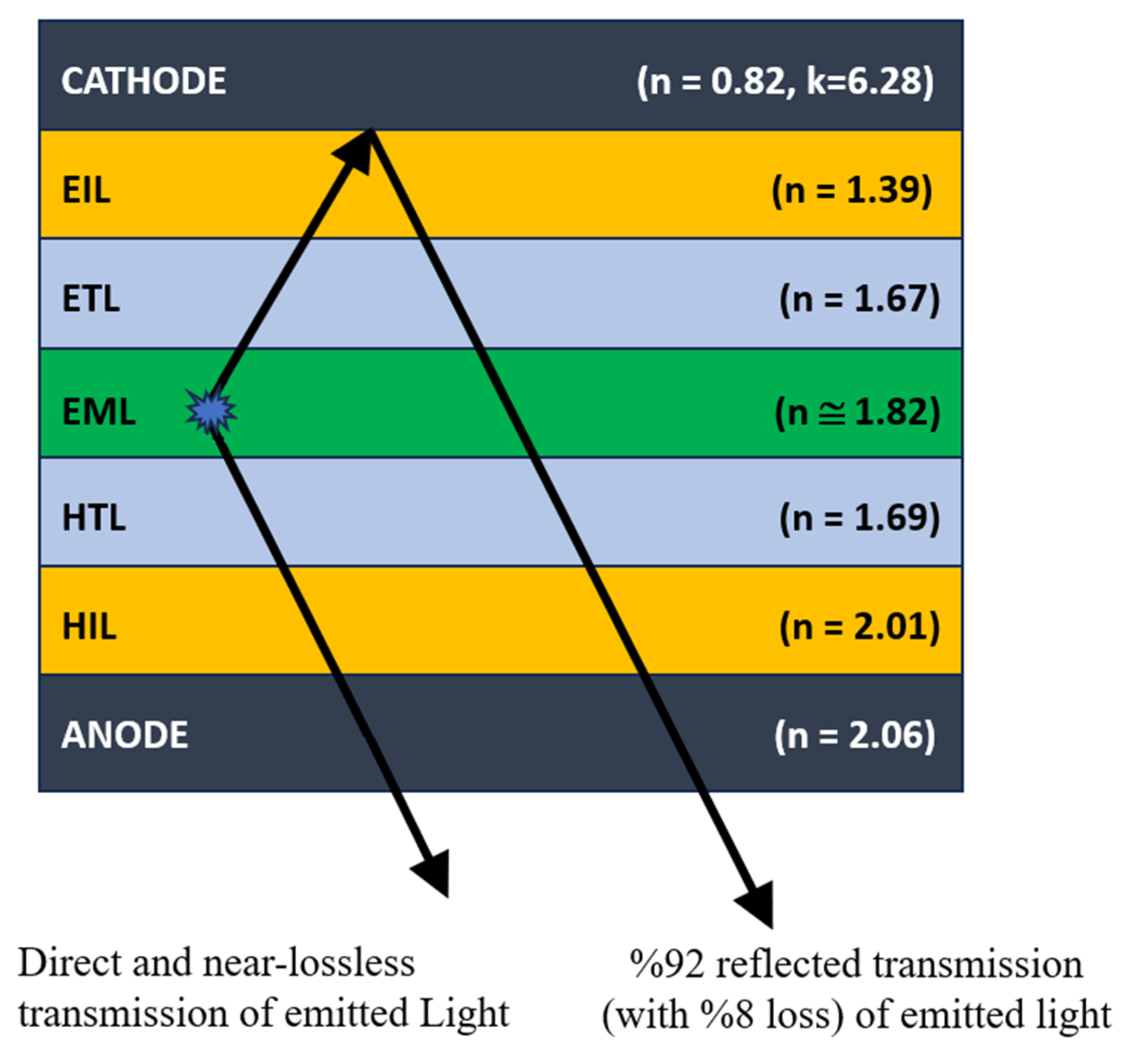
2.1. Modelling of OLED Device Stack
2.2. Selection of Materials for Each Layer for Optimal Electron–Hole Balance
2.3. Calculation of Effective Reflectivity of Multiple OLED Layers
3. Results and Discussions
3.1. SETFOS Simulation Results: Impact of Layers on OLED Characteristics
3.1.1. The Effect of OLED Layers on Color Coordinates
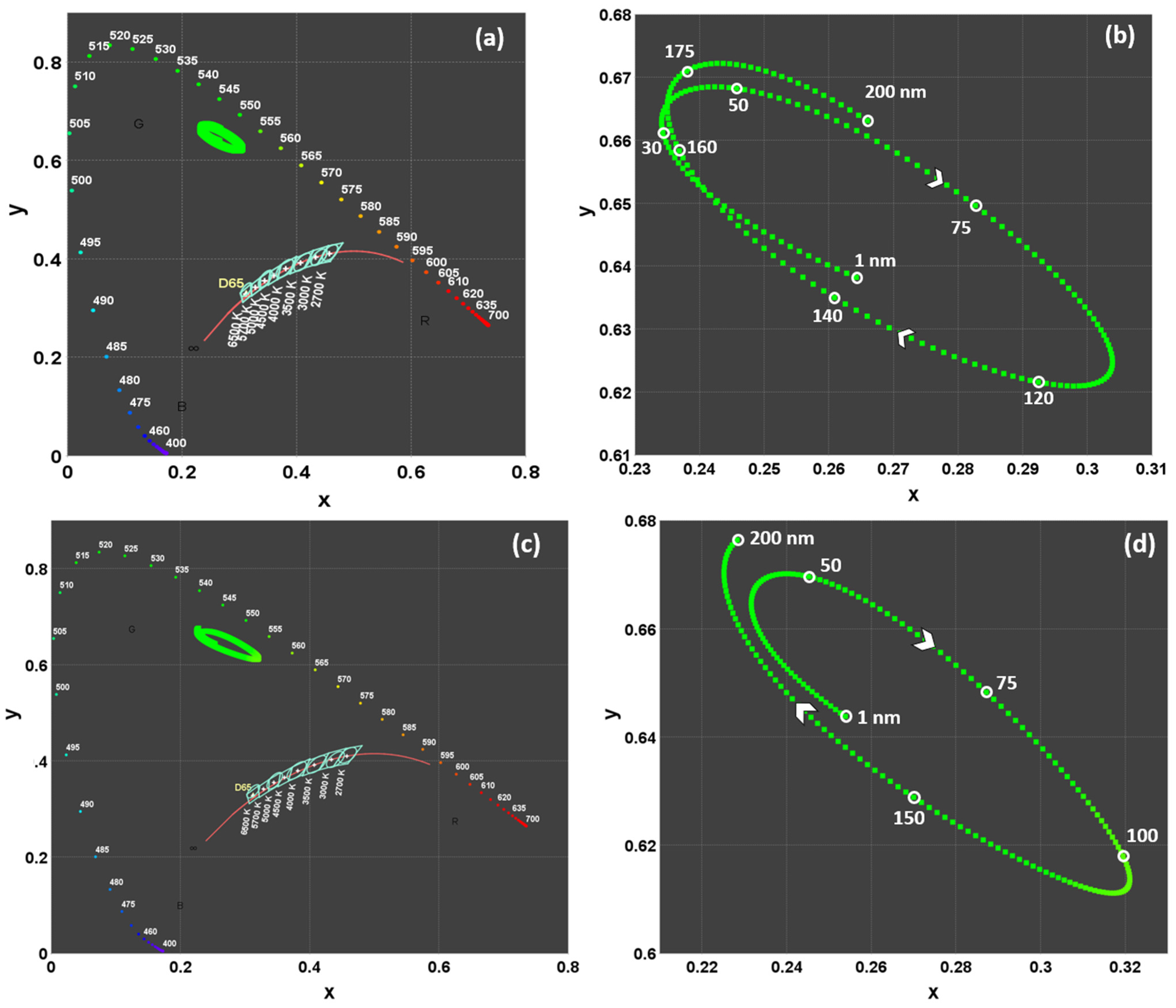
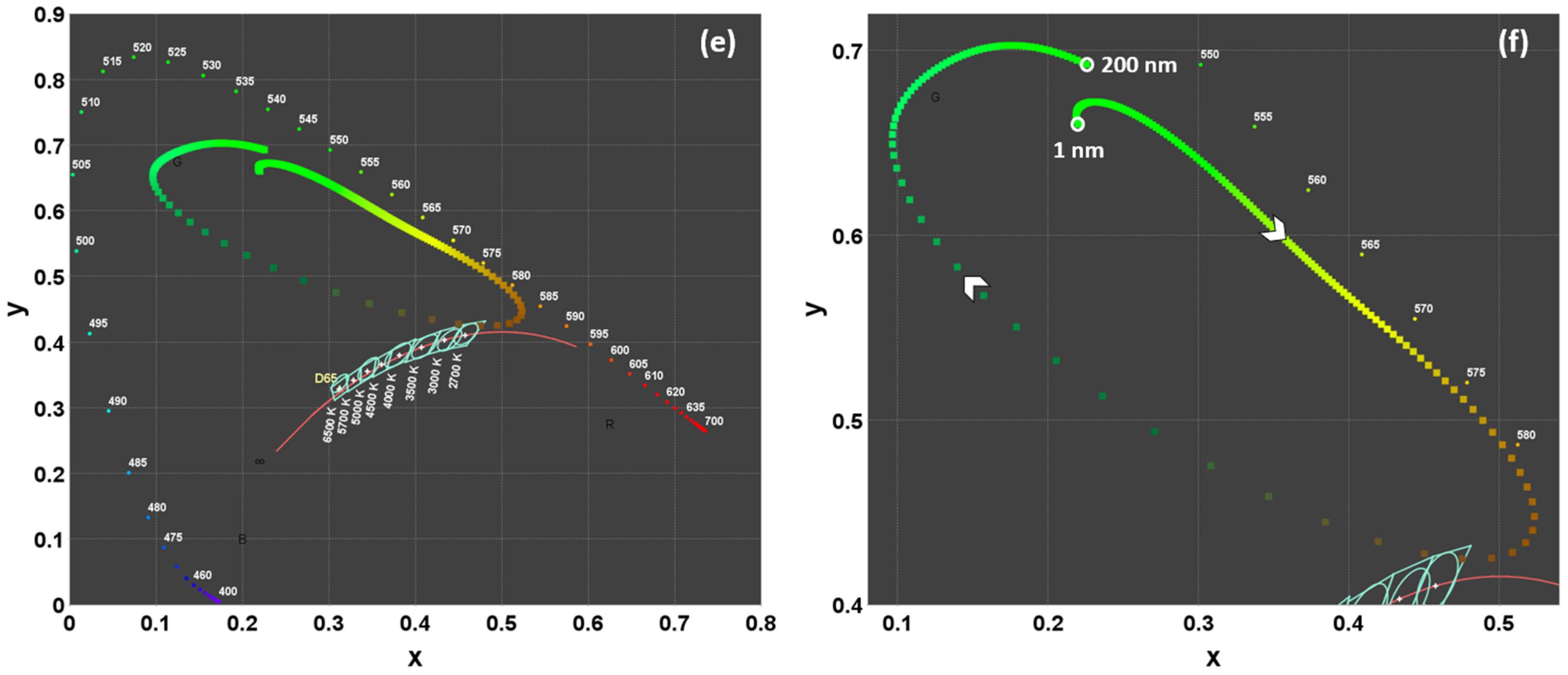
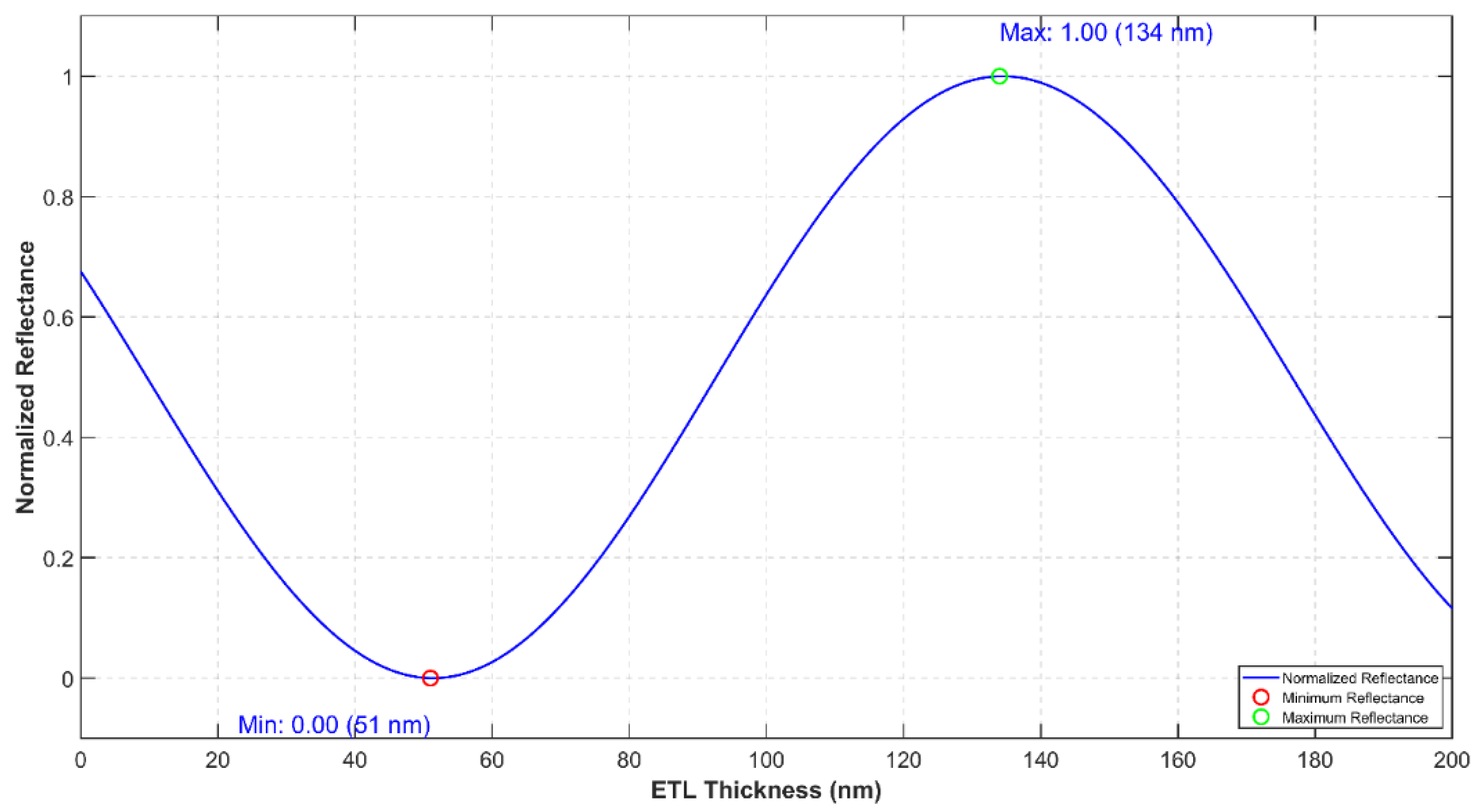
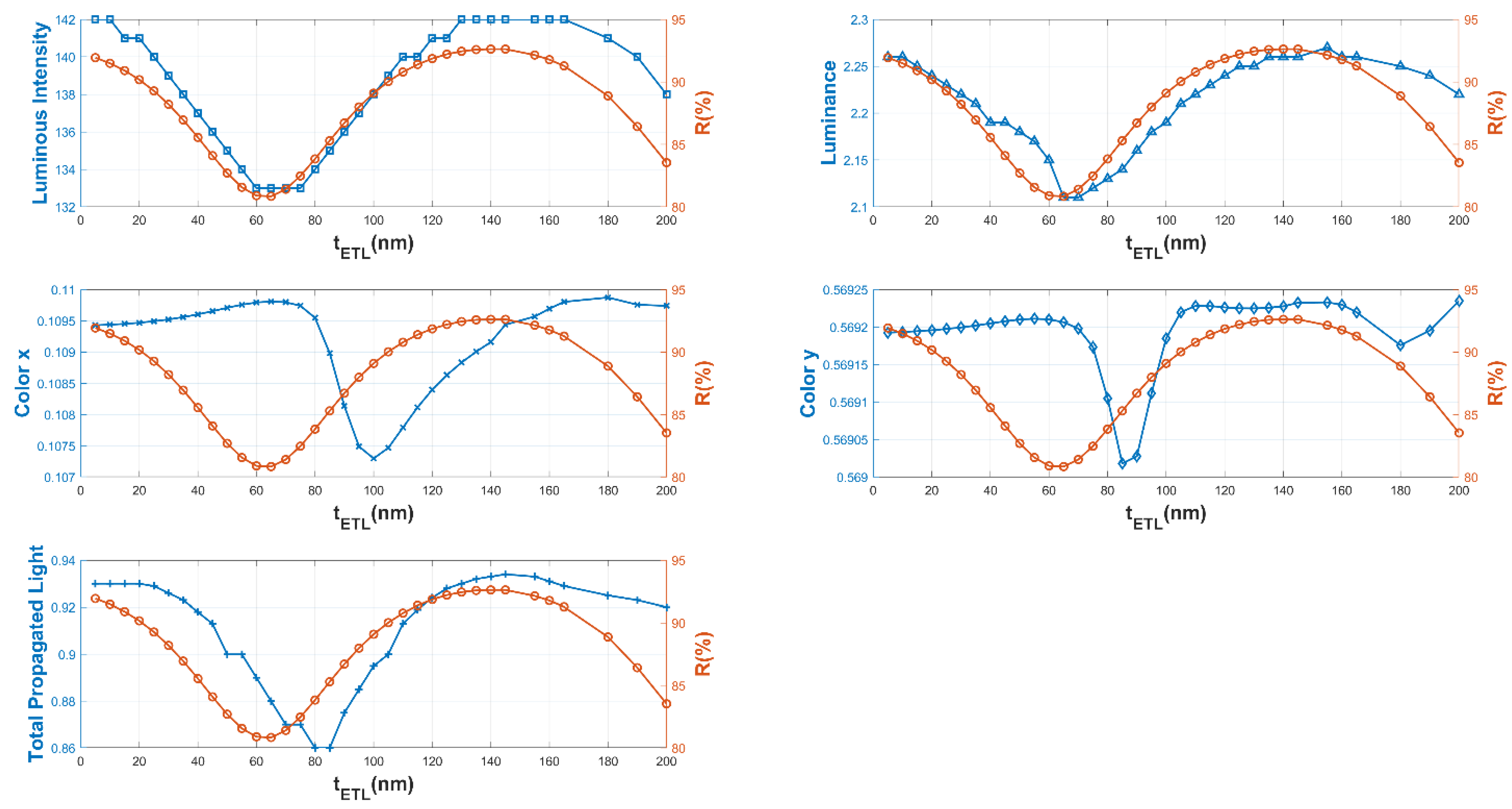
3.1.2. The Effect of Layer Thickness on Color Coordinates
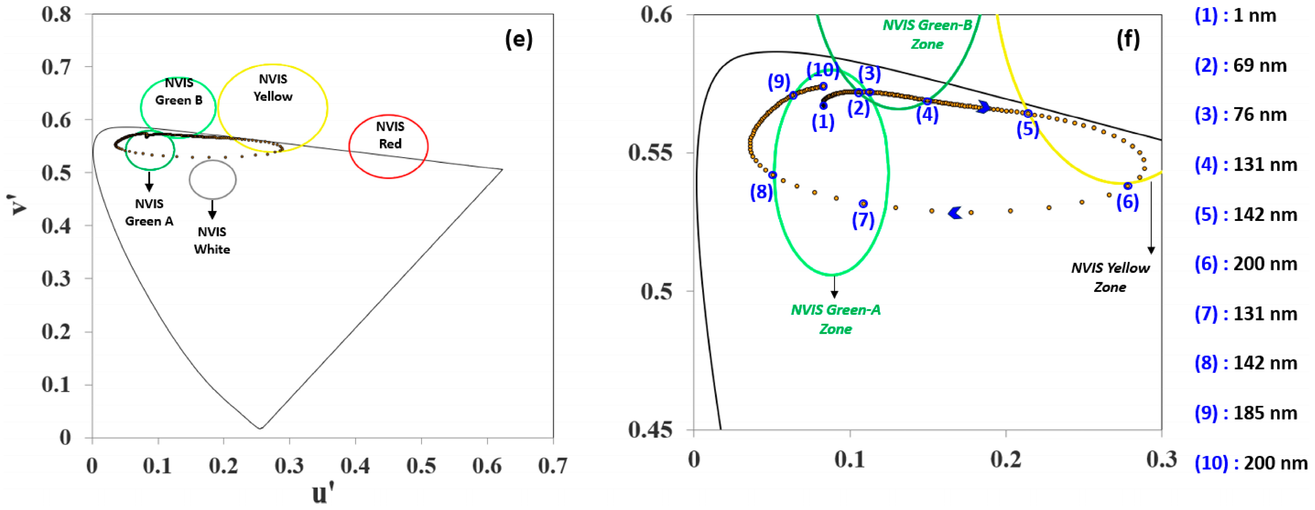
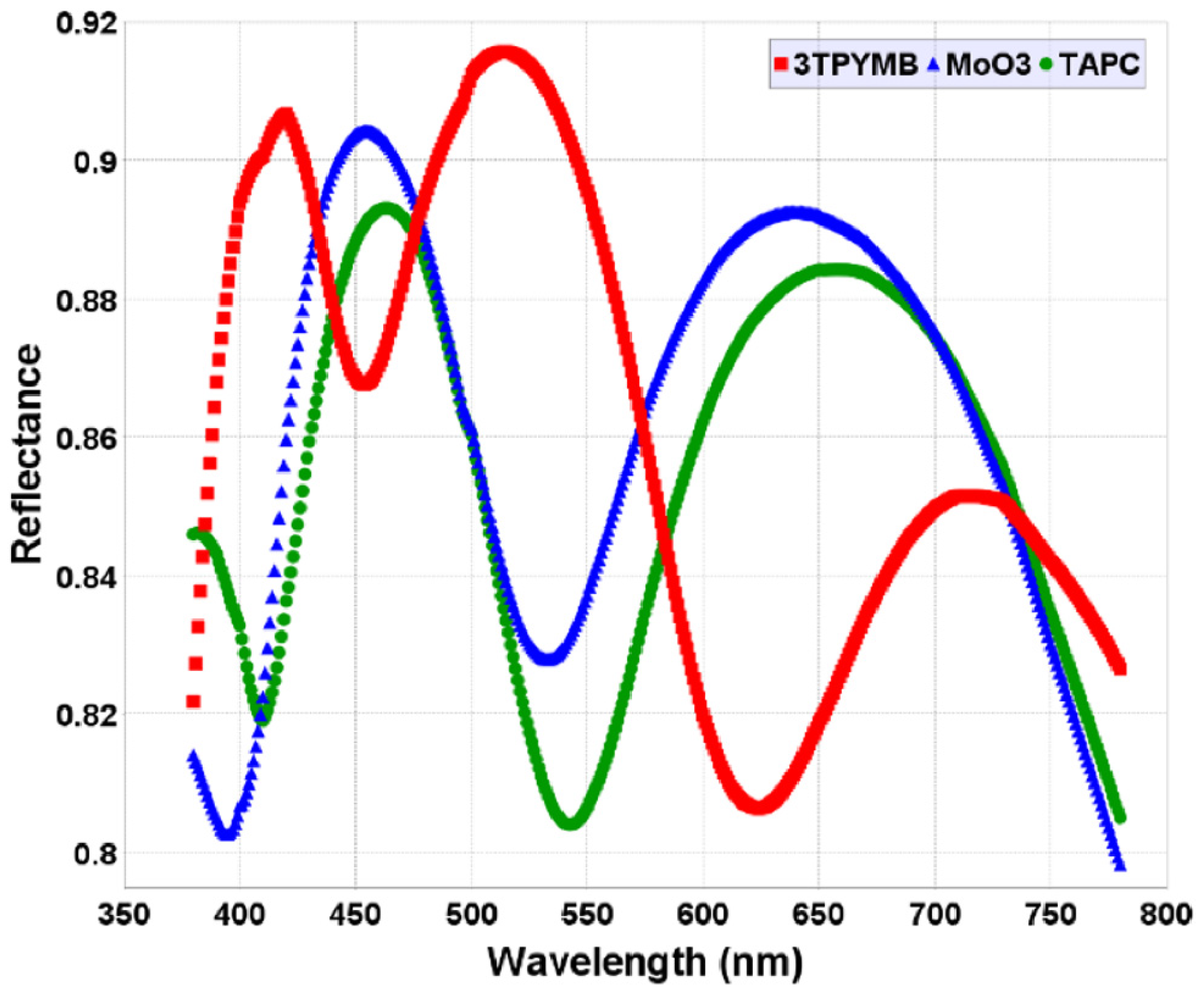
3.1.3. Effect of the Reflectivities of the Layer Materials on Luminance and Color Coordinates
3.2. Model Validation
3.3. Model Validation Using LightTools
4. Conclusions
Supplementary Materials
Author Contributions
Funding
Data Availability Statement
Conflicts of Interest
References
- Kawamoto, H. The history of liquid-crystal displays. Proc. IEEE 2002, 90, 460–500. [Google Scholar] [CrossRef]
- Kawamoto, H. The History of Liquid-Crystal Display and Its Industry. In Proceedings of the 3rd IEEE HISTory of ELectro-technology CONference—“The Origins of Electrotechnologies” (HISTELCON 2012), Pavia, Italy, 5–7 September 2012; pp. 1–6. [Google Scholar]
- Rabbani, S.A.; Ahmed, M.; Zahid, A.H. E-Ink; Revolution of Displays. MATEC Web Conf. 2023, 381, 02003. [Google Scholar] [CrossRef]
- Chiu, H.-J.; Lo, Y.-K.; Lee, T.-P.; Mou, S.-C.; Huang, H.-M. Design of an RGB LED Backlight Circuit for Liquid Crystal Display Panels. IEEE Trans. Ind. Electron. 2009, 56, 2793–2795. [Google Scholar] [CrossRef]
- Mahon, J.K.; Brown, J.J.; Hack, M.G.; Hewitt, R.H.; Huffman, D.C. OLED Displays for Military Applications. AeroSense 2000, 4022, 233–240. [Google Scholar]
- Hack, M.; Chwang, A.; Tung, Y.-J.; Hewitt, R.; Brown, J.; Lu, J.; Shih, C.; Ho, J.; Street, R.A.; Moro, L.; et al. Status and Opportunities for High Efficiency OLED Displays on Flexible Substrates. MRS Proc. 2005, 870. [Google Scholar] [CrossRef]
- Sarma, K.R. Recent progress in OLED And Flexible Displays and Their Potential for Application to Aerospace and Military Display Systems. In Display Technologies and Applications for Defense, Security, and Avionics IX; and Head- and Helmet-Mounted Displays XX; SPIE: St Bellingham, WA, USA, 2015; Volume 9470, p. 94700J. [Google Scholar]
- Sarma, K.R. Recent Advances in AM OLED Technologies for Application to Aerospace and Military Systems. In Proceedings of the Head and Helmet-Mounted Displays XVII; and Display Technologies and Applications for Defense, Security, and Avionics VI, Baltimore, MA, USA, 10 May 2021; p. 83830P. [Google Scholar]
- Trakalo, M.; Lorimer, S. The use of OLED Display Technology in Military Applications. In Proceedings of the Display Technologies and Applications for Defense, Security, and Avionics II, Orlando, FL, USA, 17 April 2008; Volume 6956, p. 69560M. [Google Scholar]
- Yadav, S.; Mittal, P.; Negi, S. Recent advancements over a decade for organic light-emitting diodes: From structural diversity, role of layers, colour emission, material classification, performance improvement, fabrication to applications. Bull. Mater. Sci. 2022, 45, 1–26. [Google Scholar] [CrossRef]
- Kang, C.-M.; Lee, H. Recent progress of organic light-emitting diode microdisplays for augmented reality/virtual reality applications. J. Inf. Disp. 2021, 23, 19–32. [Google Scholar] [CrossRef]
- Desjardins, D.D.; Hopper, D.G. Defense Display Market Assessment. In Proceedings of the Aerospace/Defense Sensing and Controls, Orlando, FL, USA, 14 September 1998; pp. 21–32. [Google Scholar]
- Giuglianotti, M.J.; Doyle, J.J.J.; Wisler, K.T. MIL-L-85762 as Applied to Liquid Crystal Displays. In Proceedings of the SPIE’s International Symposium on Optical Engineering and Photonics in Aerospace Sensing, Orlando, FL, USA, 4–8 April 1994; pp. 242–247. [Google Scholar]
- Khan, A.A.; Davis, D.J.; Huang, X.-Y.; Miller, N.; Jones, C.M.; Doane, J.W. Novel bistable reflective cholesteric liquid crystal display device for use with night vision goggles. In Proceedings of the Cockpit Displays V: Displays for Defense Applications, Orlando, FL, USA, 13–17 April 1998; pp. 210–216. [Google Scholar]
- Task, H.L.; Marasco, P.L. The Impact of Changing Night Vision Goggle Spectral Response on Night Vision Imaging System Lighting Compatibility. In Proceedings of the Helmet- and Head-Mounted Displays IX: Technologies and Applications, Orlando, FL, USA, 8 September 2004; pp. 64–72. [Google Scholar]
- Grabski, G.; Yugawa, K. Recent trends in NVIS requirements. In Proceedings of the International Display Research Conference, Edinburgh, UK, 22–25 September 2005. [Google Scholar]
- Mil-Std-3009; Interface Standard Lighting, Aircraft, Night Vision Imaging Sys-Tem (Nvis) Compatible. Department of Defense: Arlington County, VA, USA, 2001. Available online: http://www.everyspec.com (accessed on 30 January 2025).
- Robinson, T.; Green, J.; Jacobson, M.; Grabski, G. Flight Instruments and Helmet-Mounted Swir Imaging systems. In Proceedings of the Display Technologies and Applications for Defense, Security, and Avionics V and Enhanced and Synthetic Vision, Orlando, FL, USA, 10 May 2011; p. 804205. [Google Scholar]
- Phipps, B.; Gaudette, C.; Young, S. Proceedings of the Ruggedized Color AMLCD and LED Backlight Illumination for Night Vision Applications, 49th Annual SID Symposium, Seminar, and Exhibition. Los Angeles, CA, USA, 15–20 May 2011. [Google Scholar] [CrossRef]
- Kaçar, R.; Serin, R.B.; Uçar, E.; Ülkü, A. Removing crosstalk effect for high efficient polymer light emitting diode display. Solid-State Electron. 2022, 192, 108253. [Google Scholar] [CrossRef]
- MIL-L-85762a; Lighting, Aircraft, Interior, Night Vision Imaging System (NVIS) Compatible. Department of Defense: Arlington County, VA, USA, 1988.
- CIE. “Colorimetry—Part 5: CIE 1976 L*u*v* Colour Space And U’, V’ Uniform Chromaticity Scale Diagram”. International Comission on İllumination. Available online: https://cie.co.at/publications/colorimetry-part-5-cie-1976-luv-colour-space-and-u-v-uniform-chromaticity-scale-1 (accessed on 20 January 2025).
- Tchon, J.L.; Barnidge, T.J.; Hufnagel, B.D.; Bahadur, B. Current state of OLED technology relative to military avionics requirements. In Proceedings of the Display Technologies and Applications for Defense, Security, and Avionics VIII and Head- and Helmet-Mounted Displays XIX, Baltimore, MD, USA, 13 June 2014; p. 90860H. [Google Scholar]
- Davis, J.V.; Kramer, S.W. Thermal Management for Extend OLED and Micro LED Avionics Life. U.S. Patent 10278312B1, 30 April 2019. [Google Scholar]
- Desjardins, D.D.; Meyer, F.M. Military Display Performance Parameters. In Proceedings of the Head- and Helmet-Mounted Displays XVII and Display Technologies and Applications for Defense, Security, and Avionics VI, Baltimore, MD, USA, 23 May 2021; p. 838310. [Google Scholar]
- Boulter, B.E.; Bowyer, R.L. New NVIS Compatibility Standard Evaluated. In Proceedings of the of SPIE. 2001, Volume 4362. Available online: https://www.spiedigitallibrary.org/conference-proceedings-of-spie/4362/1/New-NVIS-compatibility-standard-evaluated/10.1117/12.439133.short/ (accessed on 30 January 2025).
- Dunn, W.; Presley, H.; Tran, C. NVIS Compatible Backlight Device and Electronic Display Using the Same. U.S. Patent 10,705,286, 7 July 2019. [Google Scholar]
- Negi, S.; Mittal, P.; Kumar, B. In-Depth Analysis of Structures, Materials, Models, Parameters, and Applications of Organic Light-Emitting Diodes. J. Electron. Mater. 2020, 49, 4610–4636. [Google Scholar] [CrossRef]
- Negi, S.; Mittal, P.; Kumar, B. Analytical modelling and parameters extraction of multilayered OLED. IET Circuits Devices Syst. 2019, 13, 1255–1261. [Google Scholar] [CrossRef]
- Yadav, S.; Mittal, P.; Negi, S. Review—Advancements and Perspectives of Organic LED: In Depth Analysis of Architectural Design, Characteristics Parameters, Fabrication Techniques, and Applications. ECS J. Solid State Sci. Technol. 2023, 12, 046004. [Google Scholar] [CrossRef]
- Negi, S.; Mittal, P.; Kumar, B. Impact of different layers on performance of OLED. Microsyst. Technol. 2018, 24, 4981–4989. [Google Scholar] [CrossRef]
- Wang, W.; Li, H.; Huang, D.; Wang, X.; Wang, Y.; Chen, Y.; Yi, M.; Cheng, Q.; Song, Y.; Han, G. High-Efficiency Tandem OLED with Multiple Buffer Layers to Enhance Electron Injection and Transmission. J. Electron. Mater. 2023, 52, 5287–5296. [Google Scholar] [CrossRef]
- Poriel, C.; Rault-Berthelot, J. Designing Host Materials for the Emissive Layer of Single-Layer Phosphorescent Organic Light-Emitting Diodes: Toward Simplified Organic Devices. Adv. Funct. Mater. 2021, 31, 2010547. [Google Scholar] [CrossRef]
- Lucas, F.; Brouillac, C.; Fall, S.; Zimmerman, N.; Tondelier, D.; Geffroy, B.; Leclerc, N.; Heiser, T.; Lebreton, C.; Jacques, E.; et al. Simplified Green-Emitting Single-Layer Phosphorescent Organic Light-Emitting Diodes with an External Quantum Efficiency > 22%. Chem. Mater. 2022, 34, 8345–8355. [Google Scholar] [CrossRef]
- Sandrez, S.; Della-Gatta, S.M.; Maindron, T. Impact of pixel surface topography onto thin-film encapsulated top-emitting organic light-emitting diodes performances. Thin Solid Films 2020, 699, 137869. [Google Scholar] [CrossRef]
- Cooper, E.A.; Jiang, H.; Vildavski, V.; Farrell, J.E.; Norcia, A.M. Assessment of OLED displays for vision research. J. Vis. 2013, 13, 16. [Google Scholar] [CrossRef] [PubMed]
- Wanat, R.; Mantiuk, R.K. Simulating and compensating changes in appearance between day and night vision. ACM Trans. Graph. 2014, 33, 1–12. [Google Scholar] [CrossRef]
- Nguyen, V.H.; Pham, V.H.; Cui, X.; Ma, M.; Kim, H. Design and evaluation of features and classifiers for OLED panel defect recognition in machine vision. J. Inf. Telecommun. 2017, 1, 334–350. [Google Scholar] [CrossRef]
- Jou, J.-H.; Singh, M.; Su, Y.-T.; Liu, S.-H.; He, Z.-K. Blue-hazard-free Candlelight OLED. J. Vis. Exp. 2017, 19, e54644. [Google Scholar] [CrossRef]
- Ye, Z.; Ling, Z.; Chen, M.; Yang, J.; Wang, S.; Zheng, Y.; Wei, B.; Li, C.; Chen, G.; Shi, Y. Low energy consumption phosphorescent organic light-emitting diodes using phenyl anthracenone derivatives as the host featuring bipolar and thermally activated delayed fluorescence. RSC Adv. 2019, 9, 6881–6889. [Google Scholar] [CrossRef]
- Lin, C.-H.; Kang, C.-K.; Hsiu, P.-C. Catch Your Attention: Quality-Retaining Power Saving on Mobile OLED displays. In Proceedings of the DAC’14, 51st Annual Design Automation Conference, San Fransisco, CA, USA, 1–5 June 2014; pp. 1–6. [Google Scholar]
- Zhao, L.; Jiang, X.; Lang, J.; Jiang, W.; Zhang, G.; Xue, C.; Zheng, L.; Zhao, S. The influence of the Rubrene thickness on the performance of white organic light-emitting devices. Mater. Express 2020, 10, 384–388. [Google Scholar] [CrossRef]
- Guo, K.; Wang, S.; Si, C.; Wang, T.; Zhang, J.; Chen, C.; Jing, Y.; Yang, L.; Chen, G.; Wei, B. Carrier transfer and luminescence characteristics of thickness-dependent organic light-emitting diodes using transporting material as the host of emitting layer. Phys. Status Solidi (a) 2017, 214, 1600689. [Google Scholar] [CrossRef]
- Mokhtar, M.S.A.M.; Yap, C.C.; Salleh, M.M.; Umar, A.A.; Yahaya, M. The Effects of Mixed Electroluminescent (EL) Polymer Layer Thickness on The Single Layer Organic Light Emitting Diode (OLED) Performance. In Proceedings of the 10th IEEE International Conference on Semiconductor Electronics (ICSE), Kuala Lumpur, Malaysia, 19–21 September 2012; pp. 759–762. [Google Scholar]
- Kumar, P.; Agrawal, N.; Pandey, V.; Gautam, A.; Sharma, S.; Chaudhary, S. Highly-efficient OLED with cesium fluoride electron injection layer. Solid State Electron. 2021, 183, 108031. [Google Scholar] [CrossRef]
- Gadirov, R.M.; Odod, A.V.; Kurtsevich, A.E.; Ilgach, D.M.; Yakimansky, A.V.; Kopylova, T.N. Multilayer Light-Emitting Diodes Based on Organic Semiconductor Polymers. Russ. Phys. J. 2018, 61, 1541–1546. [Google Scholar] [CrossRef]
- Matsushima, T.; Bencheikh, F.; Komino, T.; Leyden, M.R.; Sandanayaka, A.S.D.; Qin, C.; Adachi, C. High performance from extraordinarily thick organic light-emitting diodes. Nature 2019, 572, 502–506. [Google Scholar] [CrossRef] [PubMed]
- Qasim, K.; Chen, J.; Lei, W.; Li, Z.; Pan, J.; Li, Q.; Xia, J.; Tu, Y. Influence of Layer Thickness on the Performance of Quantum Dots Light Emitting Devices. SID Symp. Dig. Tech. Pap. 2014, 45, 63–66. [Google Scholar] [CrossRef]
- Liu, G.; Liu, Y.; Li, B.; Zhou, X. Influence of electron transport layer thickness on optical properties of organic light-emitting diodes. J. Appl. Phys. 2015, 117, 4922119. [Google Scholar] [CrossRef]
- Kim, J.-H.; Ju, S.-H. Emission Characteristics of Dual-Side Emission OLED with Al Cathode Thickness Variation. J. Korean Inst. Surf. Eng. 2015, 48, 174–178. [Google Scholar] [CrossRef]
- Zhang, W.; Yu, J.; Yuan, K.; Jiang, Y.; Zhang, Q.; Cao, K. Acceptor Thickness Effect of Exciplex and Electroplex Emission At Heterojunction Interface In Organic Light-Emitting Diodes. In Proceedings of the 5th International Symposium on Advanced Optical Manufacturing and Testing Technologies: Optoelectronic Materials and Devices for Detector, Imager, Display, and Energy Conversion Technology, Dalian, China, 22 October 2010; p. 76583V. [Google Scholar]
- Sharma, A.; Bhattarai, S.; Das, T.D. Fluorescent Trilayer OLED Device: An Electrical and Optical Characterization-Based SIMULATION. In Proceedings of the AIP Conference Proceedings, Hyderabad, India, 19–21 December 2019; American Institute of Physics Inc.: Melville, NY, USA, 2020; p. 030049. [Google Scholar]
- Lin, B.-Y.; Chen, C.-H.; Lin, T.-C.; Lee, J.-H.; Chiu, T.-L. Effect of Carrier-Transporting Layer on Blue Phosphorescent Organic Light-Emitting Diodes. Photonics 2021, 8, 124. [Google Scholar] [CrossRef]
- Hong, J.-W.; Kim, C.-H.; Han, H.-S.; Kang, Y.-G.; Lee, J.-Y.; Kim, T.-W. Dependence of the efficiency improvement of organic light-emitting diodes on the thickness of the Cs2CO3 electron-injection layer. J. Korean Phys. Soc. 2012, 60, 1611–1615. [Google Scholar] [CrossRef]
- Voznyak, L.; Hotra, Z.; Stakhira, P.; Cherpak, V.; Volynyuk, D.; Gorbulyk, V.; Tsizh, B. Effect of thickness of CuI hole injection layer on properties of organic light emitting diodes. Photon Lett. Pol. 2012, 4, 13. [Google Scholar] [CrossRef]
- Zhang, H.; Zhu, W.; Huang, L.; Yi, C.; Chen, R.; Chen, Y.; Li, J. A strategy of synergistic optimization: Gold and lithium co-doped vanadium oxide as a hole-injection layer for high-performance OLEDs. J. Mater. Chem. C 2022, 10, 15000–15007. [Google Scholar] [CrossRef]
- Mohan, V.; Agrawal, N.; Gautam, A.K.; Kapse, V.M.; Sazid; Rizvi, N.Z. Enabling highly-efficient OLED with solution-processed nanocrystalline copper phthalocyanine hole-injection/transport layer. Semicond. Sci. Technol. 2022, 37, 095012. [Google Scholar] [CrossRef]
- Xie, M.; Pang, H.; Wang, J.; Cui, Z.; Zheng, R.; Ding, H.; Zhang, Q.; Zhang, C.; Kwong, R.; Xia, S. High Performance Deep Red OLEDs Using Dual p-dopants to Control Hole Injection. SID Symp. Dig. Tech. Pap. 2023, 54, 100–103. [Google Scholar] [CrossRef]
- Ding, L.; Wang, J.-N.; Ni, T.; Xue, Q.; Hu, S.; Wu, R.; Luo, D.; Zheng, H.; Liu, Y.; Liu, B. Extremely-low-voltage, high-efficiency and stability-enhanced inverted bottom OLEDs enabled via a p-type/ultra-thin metal/n-doped electron injection layer. J. Mater. Chem. C 2023, 11, 2672–2679. [Google Scholar] [CrossRef]
- Kang, P.-G.; Shin, D.H.; Na, H.-Y.; Doh, Y.-J.; John, K.; Liam, S.; Suh, M.C. 38-4: The Interfacial Effect between HTL and EML on the Efficiency of Solution Processed Green Phosphorescent OLEDs. SID Symp. Dig. Tech. Pap. 2016, 47, 494–497. [Google Scholar] [CrossRef]
- Huang, J.; Pfeiffer, M.; Blochwitz, J.; Werner, A.; Salbeck, J.; Liu, S.; Leo, K. Low Operating Voltage and High Efficiency Organic Multilayer Electroluminescent Devices with p-Type Doped Hole Injection Layer. Jpn. J. Appl. Phys. 2001, 40, 6630. [Google Scholar] [CrossRef]
- Liu, M.S.; Niu, Y.-H.; Ka, J.-W.; Yip, H.-L.; Huang, F.; Luo, J.; Kim, T.-D.; Jen, A.K.-Y. Thermally Cross-Linkable Hole-Transporting Materials for Improving Hole Injection in Multilayer Blue-Emitting Phosphorescent Polymer Light-Emitting Diodes. Macromolecules 2008, 41, 9570–9580. [Google Scholar] [CrossRef]
- Shin, J.; Lee, J.Y. Hole injection control of electron blocking layer for broad recombination zone and low-efficiency roll-off in phosphorescent organic light emitting device. J. Inf. Disp. 2023, 25, 251–260. [Google Scholar] [CrossRef]
- Hu, X.; Wang, Y.; Shen, X.; Krasheninnikov, A.V.; Sun, L.; Chen, Z. 1T phase as an efficient hole injection layer to TMDs transistors: A universal approach to achieve p-type contacts. 2D Mater. 2018, 5, 031012. [Google Scholar] [CrossRef]
- Liao, Y.; Liu, X. Enhanced Performance of Organic Light Emitting Device by Dual Doping of LiF in ETL and HTL. J. Electrochem. Soc. 2010, 157, H759–H762. [Google Scholar] [CrossRef]
- Begley, W.J.; Hatwar, T.K. P-190: Novel Electron-Transporting Layer for Lowering Drive Voltage and Improving the Efficiency of OLED Devices. SID Symp. Dig. Tech. Pap. 2006, 37, 942–945. [Google Scholar] [CrossRef]
- Zhang, X.-W.; Li, J.; A Khan, M.; Zhang, L.; Jiang, X.-Y.; Haq, K.-U.; Zhu, W.-Q.; Zhang, Z.-L. Improved chromaticity and electron injection in a blue organic light-emitting device by using a dual electron-transport layer with hole-blocking function. Semicond. Sci. Technol. 2009, 24, 21. [Google Scholar] [CrossRef]
- Thelakkat, M.; Schmidt, H.W. Low Molecular Weight and Polymeric Heterocyclics as Electron Transport/Hole-blocking Materials in Organic Light-emitting Diodes. Polym. Adv. Technol. 1998, 9, 429–442. [Google Scholar] [CrossRef]
- Yadav, R.A.K.; Dubey, D.K.; Chen, S.-Z.; Liang, T.-W.; Jou, J.-H. Role of Molecular Orbital Energy Levels in OLED Performance. Sci. Rep. 2020, 10, 9915. [Google Scholar] [CrossRef]
- Jeong, B.-S. Device Modeling of Quantum Dot–Organic Light Emitting Diodes for High Green Color Purity. Appl. Sci. 2021, 11, 2828. [Google Scholar] [CrossRef]
- Jenatsch, S.; Altazin, S.; Will, P.-A.; Neukom, M.T.; Knapp, E.; Züfle, S.; Lenk, S.; Reineke, S.; Ruhstaller, B. Quantitative analysis of charge transport in intrinsic and doped organic semiconductors combining steady-state and frequency-domain data. J. Appl. Phys. 2018, 124, 105501. [Google Scholar] [CrossRef]
- Qian, M.; Shi, X.-B.; Liu, Y.; Jin, Z.-M.; Wang, X.-L.; Wang, Z.-K.; Liao, L.-S. Theoretical model for the external quantum efficiency of organic light-emitting diodes and its experimental validation. Org. Electron. 2015, 25, 200–205. [Google Scholar] [CrossRef]
- Fu, X.; Chen, Y.; Liu, D.; Zhang, J.; Lu, C. Development of Optical Films Based on Head-Mounted Display to Compensate for Gender Differences in Color Temperature of VR. Guangxue Xuebao/Acta Opt. Sin. 2021, 41, 1001. [Google Scholar] [CrossRef]
- Cheng, G.; Jiang, X.; Tang, Y.; Zhang, J.; Zhu, W.; Wu, J. Life prediction of white OLED under Weibull distribution based on MAM. Bandaoti Guangdian/Semicond. Optoelectron. 2012, 33, 715–720. [Google Scholar]
- Nhut, L.M.; Pham, T.T.; Tran, T.D.; Huan, V.D.; Shin, S. Design of Optical Collimator System for Vehicle Speed Gun using Non-Imaging Optics. Int. J. Renew. Energy Dev. 2023, 12, 366–374. [Google Scholar] [CrossRef]
- Ünlü, D.Y.; Şahin, N. M1 ve M2 aydınlatma sınıfı yollar için geliştirilen bir COB LED’li yol aydınlatma armatür modelinin optik tasarımı. J. Fac. Eng. Arch. Gazi Univ. 2023, 38, 1601–1614. [Google Scholar] [CrossRef]
- Jiali, Z.; Ping, Z.; Gang, L.; Xiangyi, W.; Chengbo, F.; Jie, G.; Yufen, Y.; Yaping, J. Stray light analysis of low-level-light optical system with LightTools software. J. Appl. Opt. 2022, 43, 4004. [Google Scholar] [CrossRef]
- Pedrotti, F.L.; Pedrotti, L.S. Introduction to Optics; Cambridge University Press (CUP): Cambridge, UK, 2017. [Google Scholar]
- Keskar, D.; Survase, S.; Thakurdesai, M. Reflectivity simulation by using transfer matrix method. J. Physics: Conf. Ser. 2021, 1913, 012051. [Google Scholar] [CrossRef]
- González-Ramírez, J.E.; Fuentes, J.; Hernández, L.C. Evaluation of the Thickness in Nanolayers Using the Transfer Matrix Method for Modeling the Spectral Reflectivity. Res. Lett. Phys. 2009, 2009, 594175. [Google Scholar] [CrossRef]
- Fujii, Y. Recent Developments in the X-Ray Reflectivity Analysis for Rough Surfaces and Interfaces of Multilayered Thin Film Materials. J. Mater. 2013, 2013, 678361. [Google Scholar] [CrossRef]
- Pfadler, T.; Stärk, M.; Zimmermann, E.; Putnik, M.; Boneberg, J.; Weickert, J.; Schmidt-Mende, L. A comparison of light-coupling into high and low index nanostructured photovoltaic thin films. APL Mater. 2015, 3, 066101. [Google Scholar] [CrossRef]


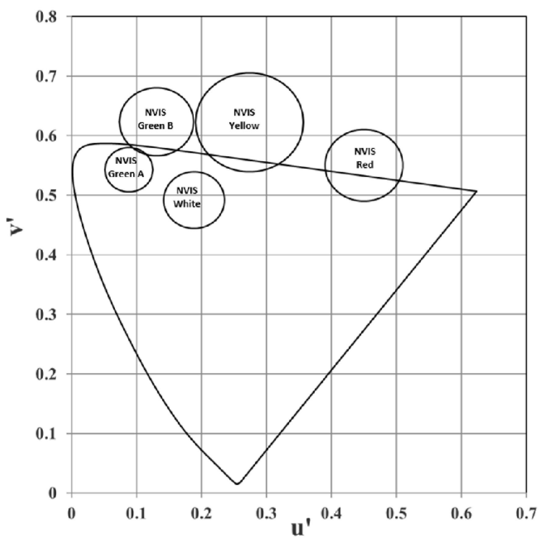
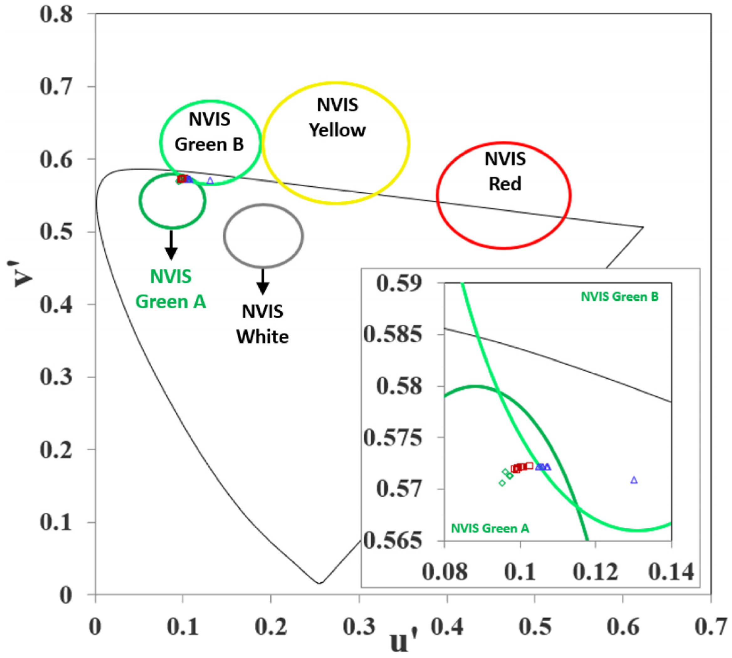
| Color | u′ | v′ | r |
| NVIS Green A | 0.088 | 0.543 | 0.037 |
| NVIS Green B | 0.131 | 0.623 | 0.057 |
| NVIS Yellow | 0.274 | 0.622 | 0.083 |
| NVIS Red | 0.450 | 0.550 | 0.060 |
| NVIS White | 0.190 | 0.490 | 0.040 |
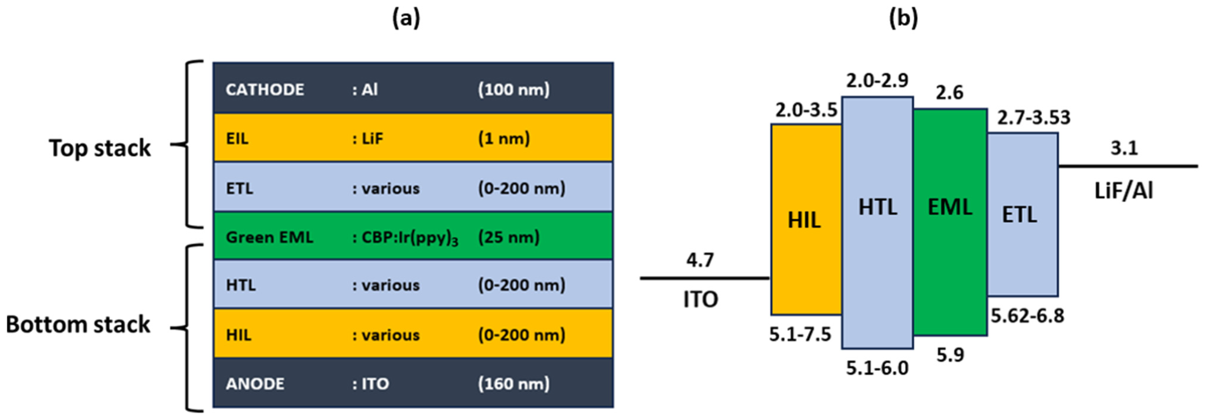
| ANODE | HIL | HTL | EML | ETL | EIL | CATHODE |
|---|---|---|---|---|---|---|
| ITO | MoO3 | NPB | CBP:Ir(ppy)3 | 3TPYMB | LiF | Al |
| CuPc | TAPC | BCP | ||||
| Alfa-NPD | Tris-PCz | BPhen | ||||
| HATCN | TCTA | TPBi | ||||
| mCP | TMPYPB | |||||
| mCBP | Balq | |||||
| CBP | B3PYMPM | |||||
| m-MTDATA | B4PYMPM | |||||
| SpiroOMeTAD | Alq3 | |||||
| 2-TNATA | Alq |
| Abbreviation | Full Name |
|---|---|
| ITO | Indium Tin Oxide |
| MoO3 | Molybdenum Trioxide |
| CuPc | Copper Phthalocyanine |
| α-NPD | N,N′-Bis(naphthalen-1-yl)-N,N′-bis(phenyl)benzidine |
| HATCN | 1,4,5,8,9,11-Hexaazatriphenylenehexacarbonitrile |
| TAPC | 1,1-Bis[4-(di-p-tolylamino) phenyl] cyclohexane |
| TCTA | Tris(4-(9H-carbazol-9-yl) phenyl) amine |
| TrisPCZ | Tris(9-phenylcarbazol-3-yl) benzene |
| NPB | N,N′-Bis(naphthalen-1-yl)-N,N′-bis(phenyl)benzidine |
| mCBP | 3,3′-Bis(N-carbazolyl)-1,1′-biphenyl |
| mCP | 1,3-Bis(N-carbazolyl) benzene |
| m-MTDATA | 4,4′,4″-Tris[3-methylphenyl(phenyl)amino] triphenylamine |
| SpiroOMeTAD | 2,2′,7,7′-Tetrakis [N,N-di(4-methoxyphenyl) amino]-9,9′-spirobifluorene |
| CBP | 4,4′-Bis(N-carbazolyl)-1,1′-biphenyl |
| 2-TNATA | 4,4′,4″-Tris(N-(naphthalen-2-yl)-N-phenylamino) triphenylamine |
| 3TPYMB | Tris[3-(3-pyridyl) mesityl] borane |
| TPBi | 1,3,5-Tris(N-phenylbenzimidazol-2-yl) benzene |
| BCP | 2,9-Dimethyl-4,7-diphenyl-1,10-phenanthroline (Bathocuproine) |
| TMPYPB | Tris[4-(pyridin-3-yl) phenyl] amine |
| BPhen | 4,7-Diphenyl-1,10-phenanthroline (Bathophenanthroline) |
| Balq | Bis(2-methyl-8-hydroxyquinolinato) aluminum (III) |
| Alq | - |
| B4PYMPM | Bis-4,6-(3,5-di(pyridin-3-yl) phenyl)-2-methylpyrimidine |
| B3PYMPM | Bis-4,6-(3-(pyridin-3-yl) phenyl)-2-methylpyrimidine |
| Alq3 | Tris(8-hydroxyquinolinato) aluminum (III) |
| LiF | Lithium Fluoride |
| Al | Aluminum |
| Layer | Layer Material | u′ | v′ | NVIS Color |
| Hole Injection | MoO3 | 0.096153 | 0.571686 | NVIS Green A |
| Hole Injection | CuPc | 0.095147 | 0.570567 | NVIS Green A |
| Hole Injection | α-NPD | 0.097469 | 0.571293 | NVIS Green A |
| Hole Injection | HATCN | 0.097223 | 0.571321 | NVIS Green A |
| Hole Transport | TAPC | 0.100431 | 0.572124 | NVIS Green A |
| Hole Transport | TCTA | 0.099879 | 0.57195 | NVIS Green A |
| Hole Transport | TrisPCZ | 0.099345 | 0.571828 | NVIS Green A |
| Hole Transport | NPB | 0.098783 | 0.57184 | NVIS Green A |
| Hole Transport | mCBP | 0.100846 | 0.572048 | NVIS Green A |
| Hole Transport | mCP | 0.100661 | 0.572045 | NVIS Green A |
| Hole Transport | m-MTDATA | 0,100754 | 0.572046 | NVIS Green A |
| Hole Transport | SpiroOMeTAD | 0.102798 | 0.572224 | NVIS Green A |
| Hole Transport | CBP | 0.099512 | 0.571944 | NVIS Green A |
| Hole Transport | 2-TNATA | 0.101059 | 0.572082 | NVIS Green A |
| Electron Transport | 3TPYMB | 0.107328 | 0.57214 | NVIS Green B |
| Electron Transport | TPBi | 0.130216 | 0.570932 | NVIS Green B |
| Electron Transport | BCP | 0.105361 | 0.572182 | NVIS Green A |
| Electron Transport | 3TMPYPB | 0.107062 | 0.572188 | NVIS Green B |
| Electron Transport | BPhen | 0.105882 | 0.57218 | NVIS Green A |
| Electron Transport | Balq | 0.107074 | 0.572168 | NVIS Green B |
| Electron Transport | B4PYMPM | 0.10491 | 0.572227 | NVIS Green A |
| Electron Transport | B3PYMPM | 0.10491 | 0.572227 | NVIS Green A |
| Electron Transport | Alq3 | 0.106045 | 0.572224 | NVIS Green B |
| Electron Transport | Alq | 0.105857 | 0.572221 | NVIS Green B |
| Layer | Refractive Index (n) | Extinction Coefficient (k) | Thickness (nm) |
|---|---|---|---|
| Cathode (Aluminum) | 0.826 | 6.28 | 100 |
| Electron Injection Layer (LiF) | 1.394095 | 0 | 1 |
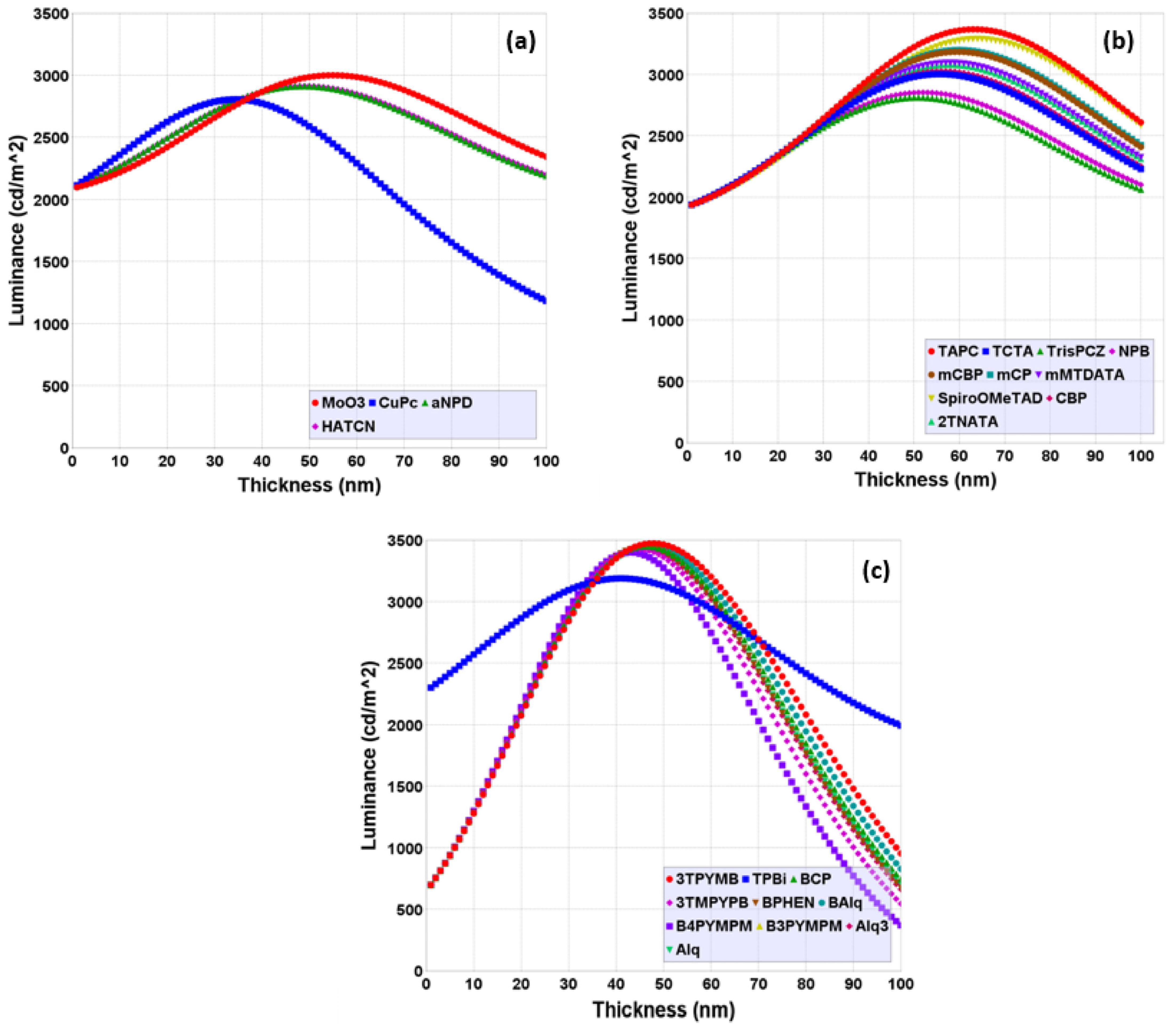
| Electron Transport Layer (3TPYMB) | 1.6677 | 0–200 | |
| Emissive Layer (CBP:Ir(ppy)3) | 1.8189 | 40 |
| Effect | Layer | % Δu′ | % Δv′ |
|---|---|---|---|
| Layer Material | Hole Injection (HIL) | 2.41 | 0.20 |
| Layer Material | Hole Transport (HTL) | 3.98 | 0.07 |
| Layer Material | Electron Transport (ETL) | 22.03 | 0.23 |
| Layer Thickness | Hole Injection (HIL) | 31.83 | 1.18 |
| Layer Thickness | Hole Transport (HTL) | 43.52 | 1.15 |
| Layer Thickness | Electron Transport (ETL) | 139.73 | 5.74 |
| Performance | HIL | HTL | ETL | %R | Lv (cd/m2) | CE (cd/A) | u′ | v′ | EQE (%) |
|---|---|---|---|---|---|---|---|---|---|
| Best (15 *) | MoO3 (55 nm) | TAPC (63 nm) | 3TPYMB (51 nm) | 92 | 3470 | 34.73 | 0.1109 | 0.5721 | 9.31 |
| Average (2 *) | CuPc (35 nm) | CBP (50 nm) | TPBi (40 nm) | 87.5 | 2800 | 28.05 | 0.0952 | 0.5706 | 7.93 |
| Worst (26 *) | CuPc (84 nm) | CBP (50 nm) | TPBi (40 nm) | 60 | 1515 | 15.15 | 0.1178 | 0.5708 | 4.27 |
Disclaimer/Publisher’s Note: The statements, opinions and data contained in all publications are solely those of the individual author(s) and contributor(s) and not of MDPI and/or the editor(s). MDPI and/or the editor(s) disclaim responsibility for any injury to people or property resulting from any ideas, methods, instructions or products referred to in the content. |
© 2025 by the authors. Licensee MDPI, Basel, Switzerland. This article is an open access article distributed under the terms and conditions of the Creative Commons Attribution (CC BY) license (https://creativecommons.org/licenses/by/4.0/).
Share and Cite
Uçar, E.; Ülkü, A.; Kaya, H.M.; Serin, R.B.; Kaçar, R.; Oral, A.Y.; Menşur, E. Impact of Layer Materials, Their Thicknesses, and Their Reflectivities on Emission Color and NVIS Compatibility in OLED Devices for Avionic Display Applications. Micromachines 2025, 16, 191. https://doi.org/10.3390/mi16020191
Uçar E, Ülkü A, Kaya HM, Serin RB, Kaçar R, Oral AY, Menşur E. Impact of Layer Materials, Their Thicknesses, and Their Reflectivities on Emission Color and NVIS Compatibility in OLED Devices for Avionic Display Applications. Micromachines. 2025; 16(2):191. https://doi.org/10.3390/mi16020191
Chicago/Turabian StyleUçar, Esin, Alper Ülkü, Halil Mert Kaya, Ramis Berkay Serin, Rifat Kaçar, Ahmet Yavuz Oral, and Ebru Menşur. 2025. "Impact of Layer Materials, Their Thicknesses, and Their Reflectivities on Emission Color and NVIS Compatibility in OLED Devices for Avionic Display Applications" Micromachines 16, no. 2: 191. https://doi.org/10.3390/mi16020191
APA StyleUçar, E., Ülkü, A., Kaya, H. M., Serin, R. B., Kaçar, R., Oral, A. Y., & Menşur, E. (2025). Impact of Layer Materials, Their Thicknesses, and Their Reflectivities on Emission Color and NVIS Compatibility in OLED Devices for Avionic Display Applications. Micromachines, 16(2), 191. https://doi.org/10.3390/mi16020191