Method for In Situ On-Wafer Tensile Test of Thin Films


Abstract
:1. Introduction
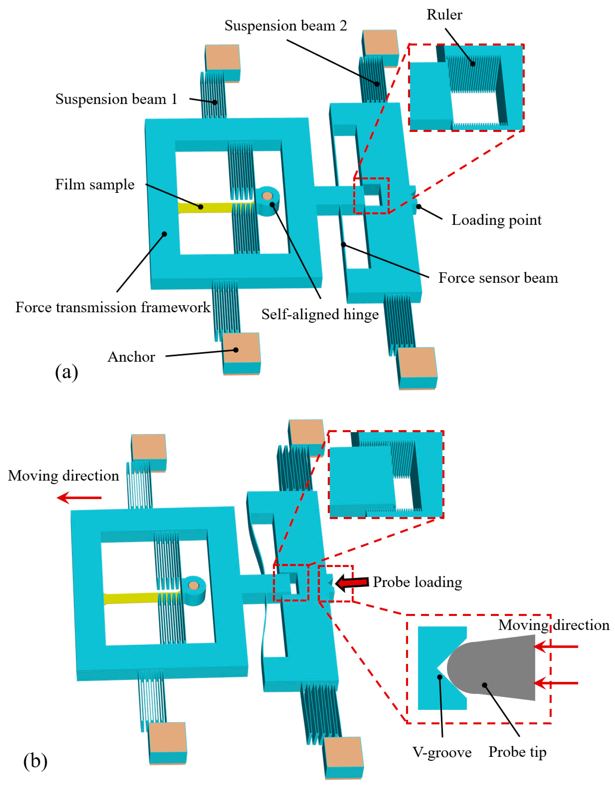
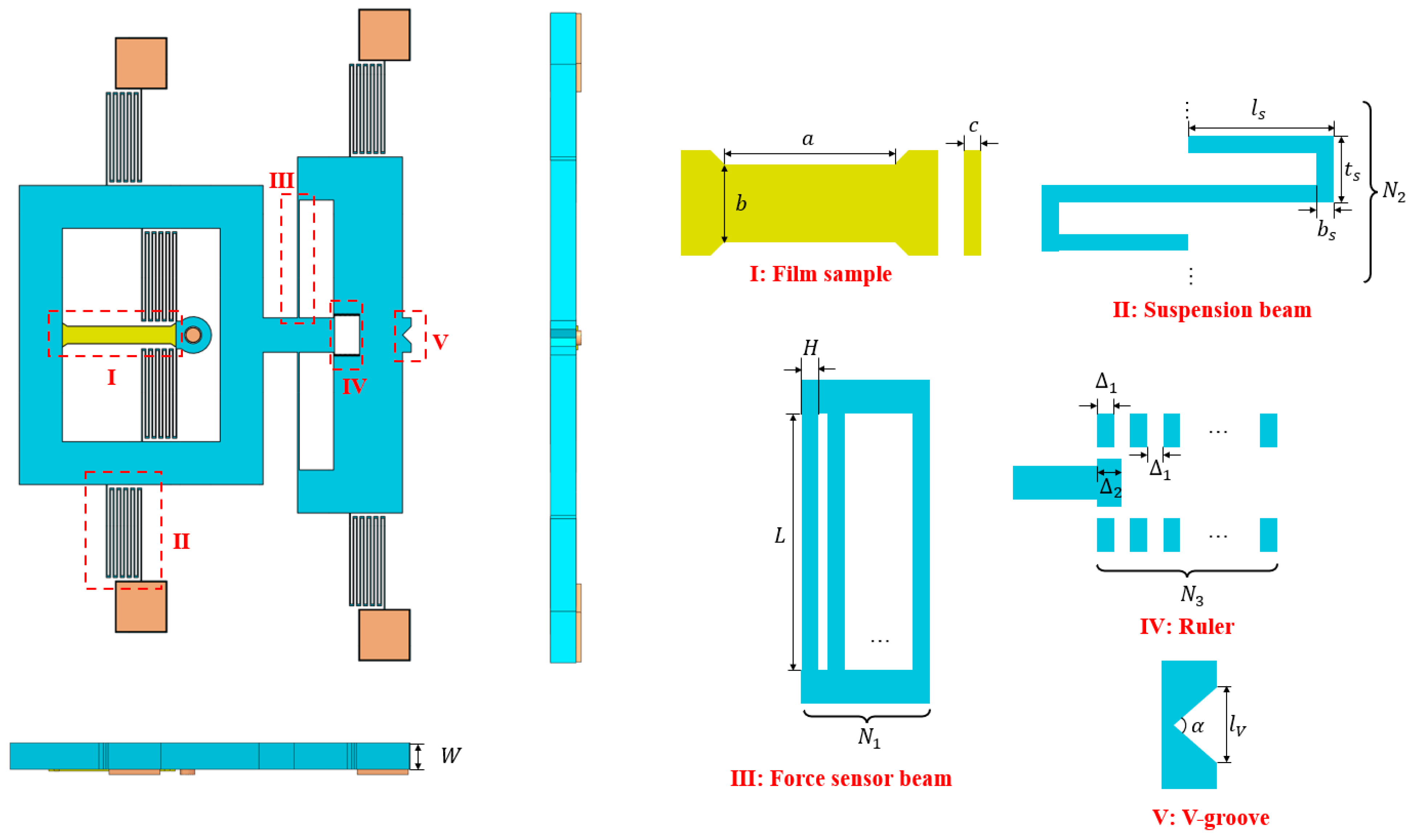
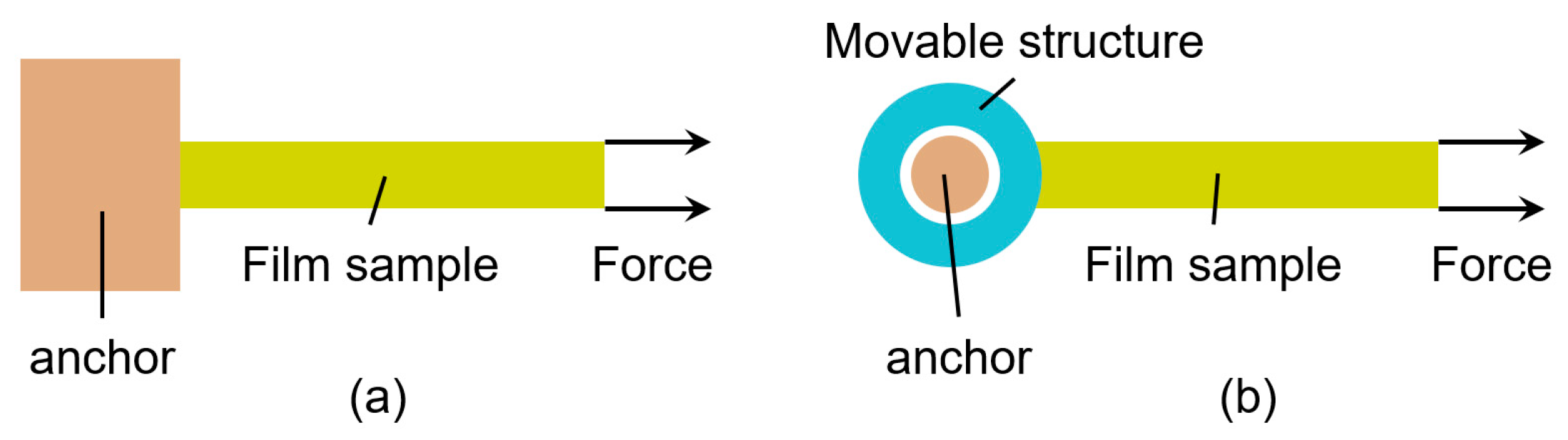
2. Structure Design
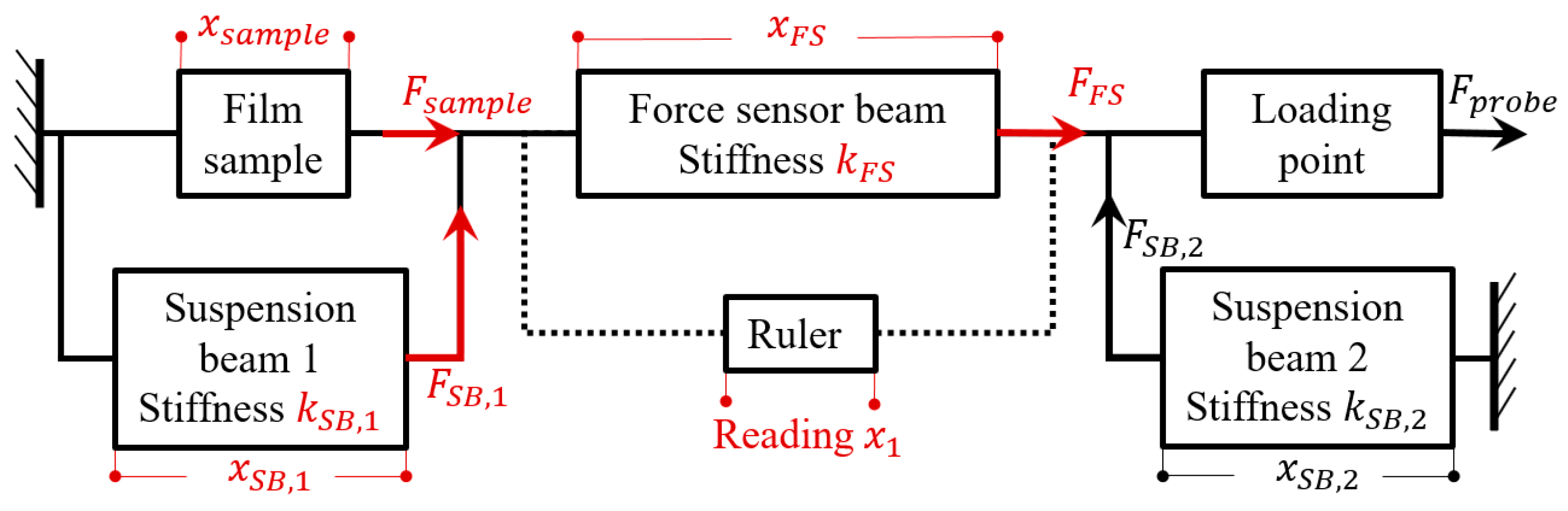
2.1. Mechanical-Lumped Model
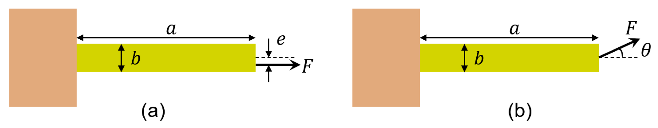
2.2. Model of Force Sensor Beam
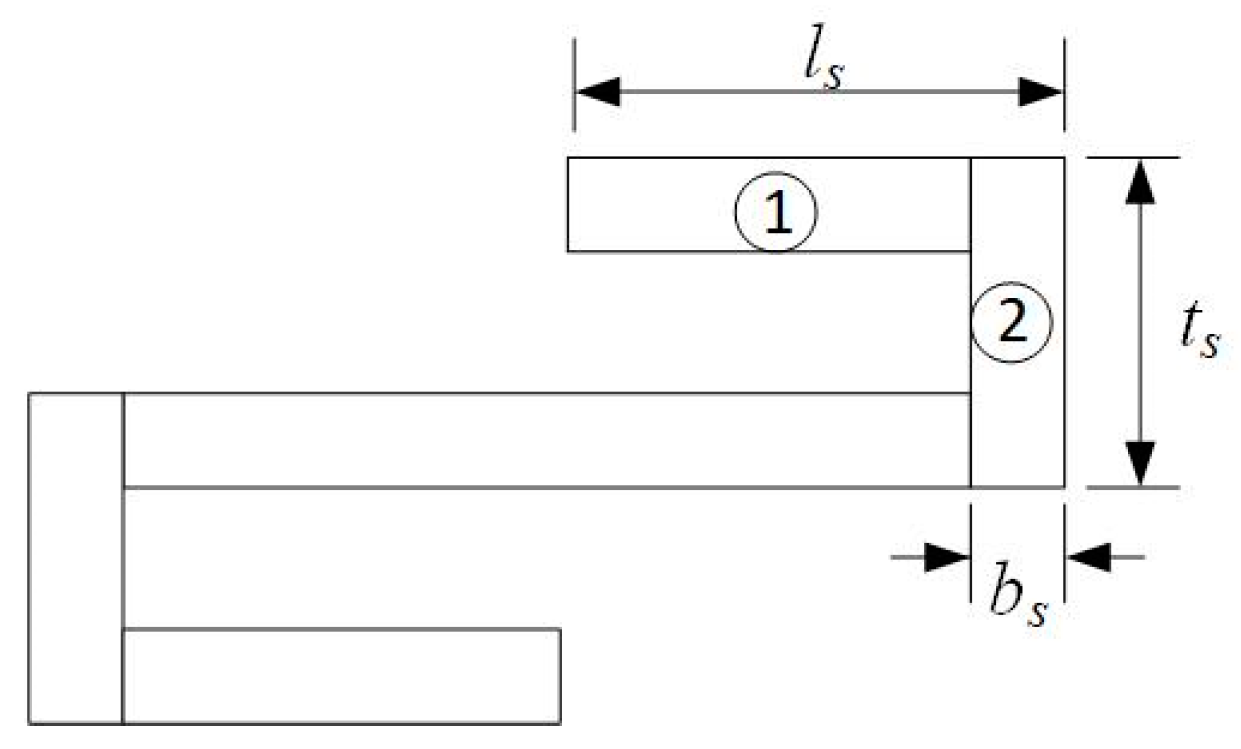
2.3. Model of Suspension Beam
2.4. Fixation of Film Sample
3. Fabrication
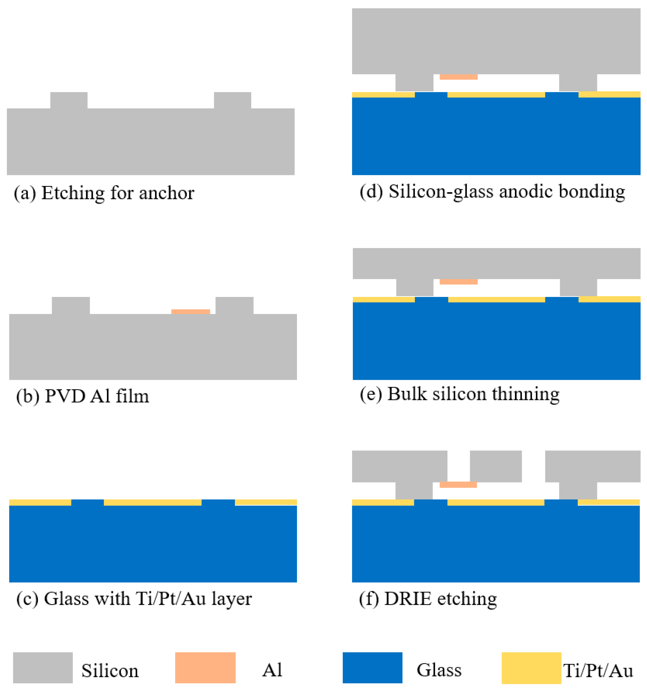
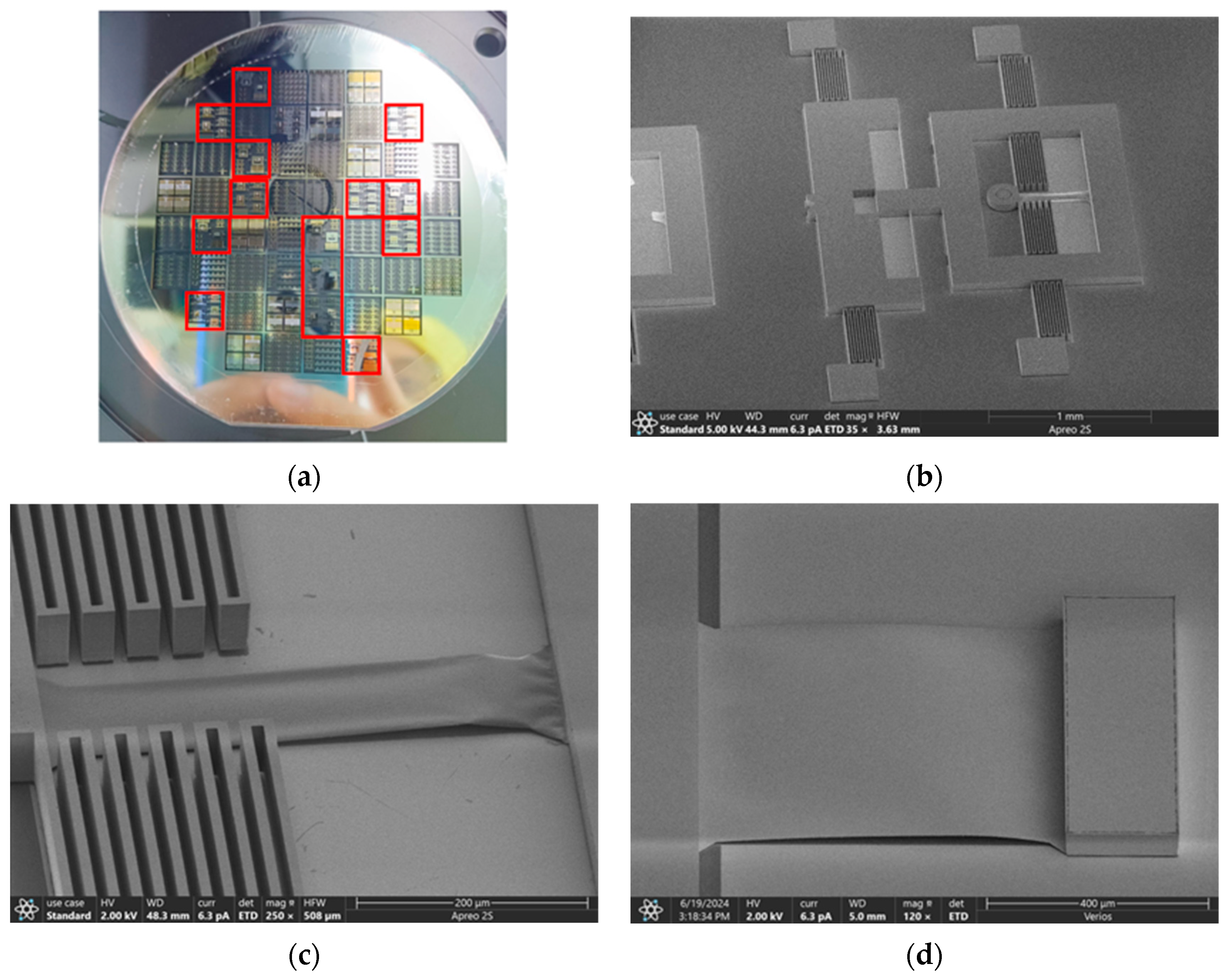
3.1. Process Flow
- The bonding surfaces of the glass and silicon wafer are positioned opposite each other and secured in a specialized alignment fixture for bonding. The fixture is then placed on the lithography machine, with the silicon wafer on top and the glass substrate underneath.
- A CCD camera located beneath the lithography machine’s stage captures the alignment marks on the silicon wafer through the glass from below and records their images on the display.
- The CCD camera automatically adjusts its focus to the glass substrate. By fine-tuning the x-axis, y-axis, and angular θ knobs, the alignment marks on the glass are aligned with those of the silicon wafer recorded on the display.
- The fixture locks the relative positions of the two substrates. The fixture is then removed from the lithography machine and transferred to the bonding machine to complete the bonding process.
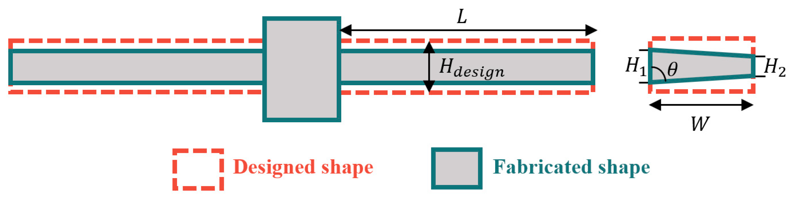
3.2. Process Error Analysis
4. Experimental Results and Discussion
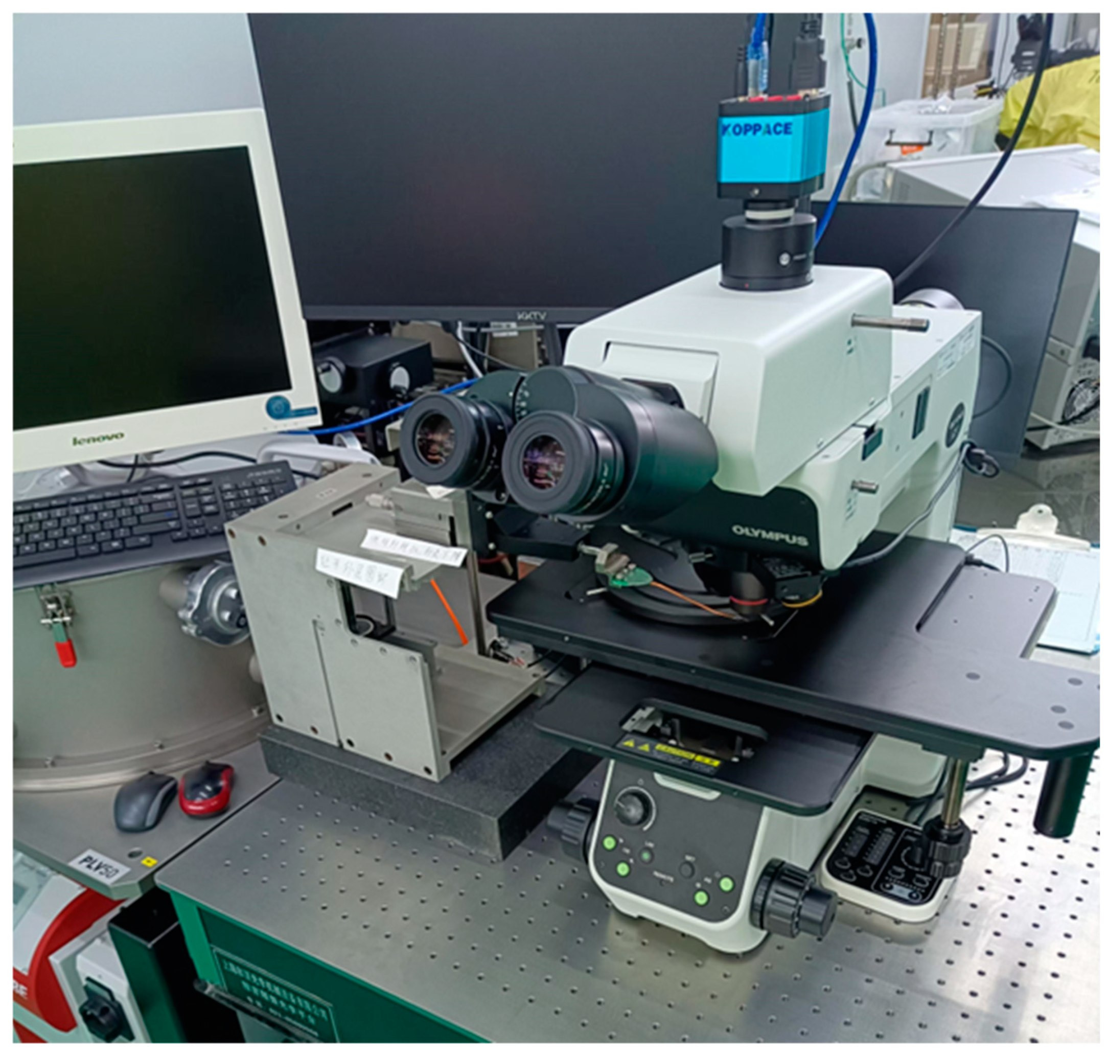
- Place the wafer to be tested on the microscope stage and level it.
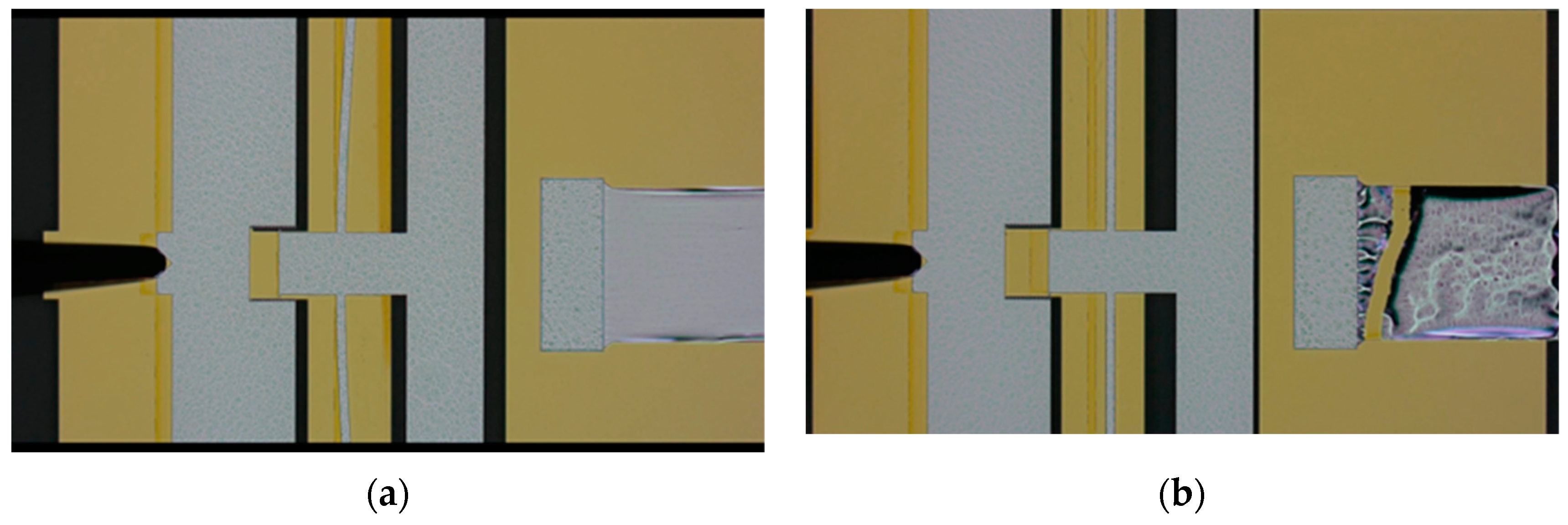
- Adjust the probe so that the probe tip is positioned at the V-groove of the probe loading point and begin video recording. Move the probe in the direction indicated in Figure 1 to drive the testing structure to apply an increasing axial tensile force to the thin film.
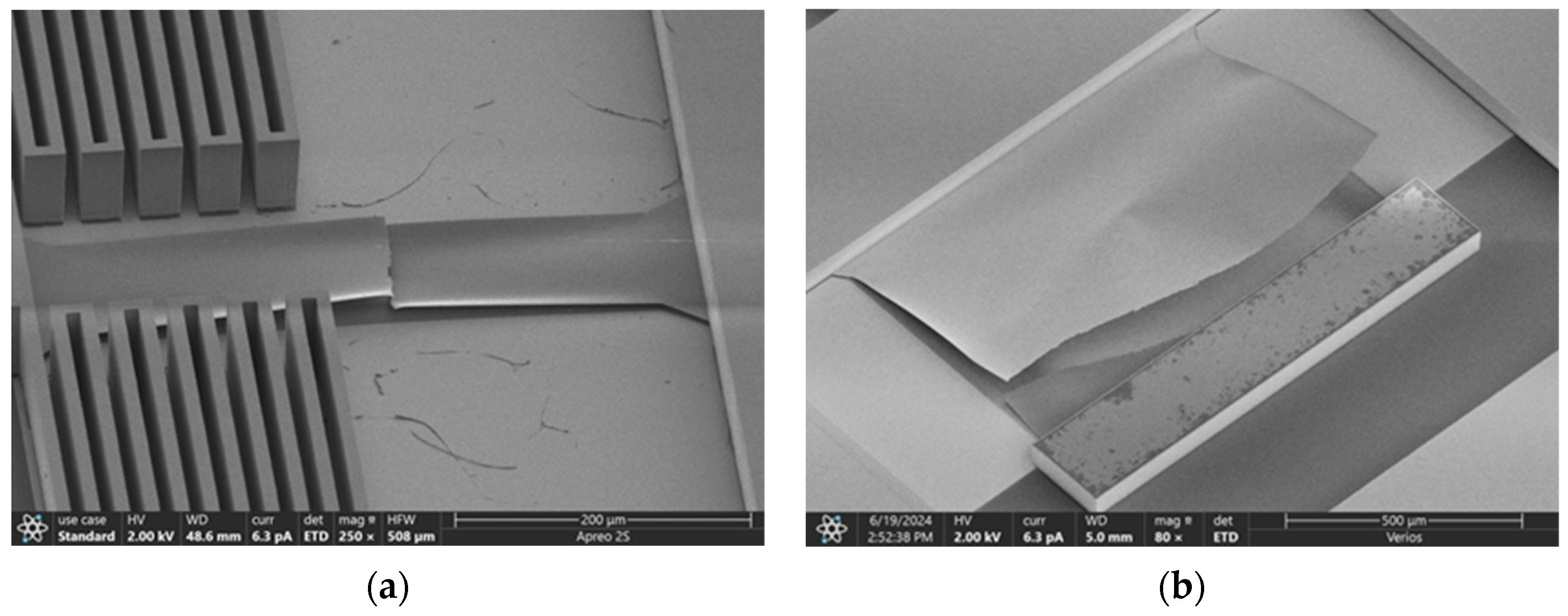
- Observe the deformation of the thin-film test structure in real-time through the microscope. Once the thin-film test structure fractures, stop the driving load and cease video recording.
- Review the video recording to read the ruler reading at the moment of fracture of the thin film.
- Substitute into the theoretical model from the previous section to calculate the tensile strength of the thin film.
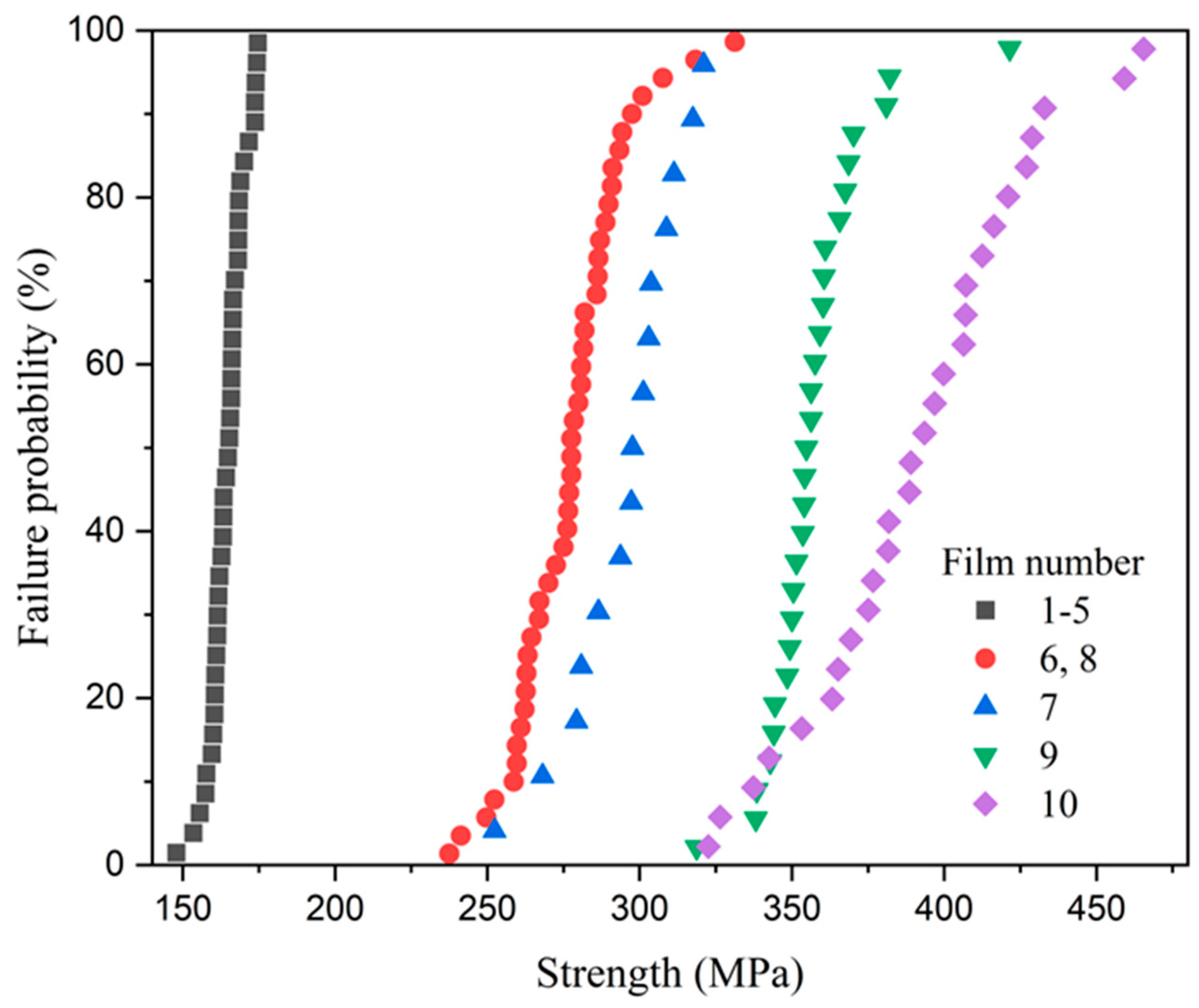
- No correlation between strength and position on the wafer was observed.
- The analysis of the strength results from Groups 1–5 reveals that the ultimate strength is independent of the film length, indicating no size effect on brittle fracture. This can be attributed to the fact that new defects initiate during the stretching process before old defects propagate, with the fracture process dominated by ductile fracture.
- Samples from Groups 1–5 exhibited immediate fracture after the elastic stage, with no distinct yield phenomenon observed. In contrast, Groups 6, 7, and 8 showed a relatively short yield stage followed by immediate fracture, with the ultimate strength approximately equal to the yield strength. Groups 9 and 10 demonstrated a more pronounced yield phenomenon, characterized by (1) a significant elongation of the aluminum film specimen, as shown in Figure 14a; (2) the ruler reading remaining relatively constant during the test, with no change in response to probe movement.
- The fracture/yield strength of the samples increased with increasing cross-sectional area. This is attributed to the following reasons: (1) wider aluminum films provide more freedom for dislocation generation and movement, exhibiting better plasticity; (2) thinner aluminum films are more affected by surface oxide layers, leading to localized stress concentration and thus a decrease in yield strength.
5. Conclusions
Author Contributions
Funding
Data Availability Statement
Conflicts of Interest
References
- Huang, X.; Zhang, D. A high sensitivity and high linearity pressure sensor based on a peninsula-structured diaphragm for low-pressure ranges. Sens. Actuat. A Phys. 2014, 216, 176–189. [Google Scholar] [CrossRef]
- Gao, C.; Zhang, D. The Establishment and Verification of the Sensitivity Model of the Piezoresistive Pressure Sensor Based on the New Peninsula Structure. J. Microelectromech. Syst. 2022, 31, 305–314. [Google Scholar] [CrossRef]
- Zhu, X.; Xie, C.; Ye, T.; Zhao, M.; Ma, J.; Jiang, J.; Niu, J.; Liu, M. Fabrication of 200 nm Period X-ray Transmission Gratings Using Electron Beam Lithography. In Proceedings of the Holography and Diffractive Optics III. International Society for Optics and Photonics, Beijing, China, 4 January 2008. [Google Scholar]
- Solgaard, O.; Godil, A.A.; Howe, R.T.; Lee, L.P.; Peter, Y.-A.; Zappe, H. Optical MEMS: From micromirrors to complex systems. J. Microelectromech. Syst. 2014, 23, 517–538. [Google Scholar] [CrossRef]
- Dehe, A. Silicon microphone development and application. Sens. Actuat. A-Phys. 2007, 133, 283–287. [Google Scholar] [CrossRef]
- Davis, J.R. Tensile Testing, 2nd ed.; ASM International: Materials Park, OH, USA, 2004; pp. 1–12. [Google Scholar]
- Stach, E.A.; Freeman, T.; Minor, A.M.; Owen, D.K.; Cumings, J.; Wall, M.A.; Chraska, T.; Hull, R.; Morris, J.; Zettl, A. Development of a Nanoindenter for In Situ Transmission Electron Microscopy. Microsc. Microanal. 2001, 7, 507–517. [Google Scholar] [CrossRef] [PubMed]
- Bellitto, V.J. Atomic Force Microscopy: Imaging, Measuring and Manipulating Surfaces at the Atomicscale, 1st ed.; InTech: Riijeka, Croatia, 2012; pp. 147–174. [Google Scholar]
- Zhu, Y.; Espinosa, H.D. An electromechanical material testing system for in situ electron microscopy and applications. Proc. Natl. Acad. Sci. USA 2005, 102, 14503–14508. [Google Scholar] [CrossRef] [PubMed]
- Brown, J.; Baca, A.; Bertness, K.; Dikin, D.; Ruoff, R.; Bright, V. Tensile measurement of single crystal gallium nitride nanowires on MEMS test stages. Sens. Actuat. A Phys. 2011, 166, 177–186. [Google Scholar] [CrossRef]
- Gianola, D.S.; Eberl, C. Micro- and nanoscale tensile testing of materials. JOM 2009, 61, 24–35. [Google Scholar] [CrossRef]
- Li, R.; Yang, F.; He, J.; Zhang, L.; Guan, T.; Fan, Z.; Cheng, L.; Zhang, D. A Universal Structure for Self-Aligned in Situ On-Chip Micro Tensile Fracture Strength Test. In Proceedings of the 2017 IEEE 30th International Conference on Micro Electro Mechanical Systems (MEMS), Las Vegas, NV, USA, 22–26 January 2017. [Google Scholar]
- Cheng, L.; Li, F.; Zhang, D. A Method for Over 100,000g Impact Test on Nanoscale Film. In Proceedings of the 2021 IEEE 34th International Conference on Micro Electro Mechanical Systems (MEMS), Online, 25–29 January 2021. [Google Scholar]
- Li, F.; Cheng, L.; Zhang, D. A Method for Biaxial Fracture Stress Test of Nanoscale film. In Proceedings of the Solid-State, Actuators and Microsystems (Transducers 2021), Online, 20–25 June 2021. [Google Scholar]
- Li, H.; Shi, G. Analysis of Application Pattern of MEMS Microspring. Chin. J. Sens. Actuator 2007, 20, 2709–2712. [Google Scholar]
- Pan, B.; Qian, K.; Xie, H. Two-dimensional digital image correlation for in-plane displacement and strain measurement: A review. Meas. Sci. Technol. 2009, 20, 062001. [Google Scholar] [CrossRef]
- Cheng, L.J. Study of Uniaxial Tensile Method for MEMS Process-Related Films. Ph.D. Thesis, Peking University, Beijing, China, 2022. [Google Scholar]
- Read, D.T.; Cheng, Y.-W.; Keller, R.R.; McColskey, J. Tensile properties of free-standing aluminum thin films. Scr. Mater. 2001, 45, 583–589. [Google Scholar] [CrossRef]
- Smithells, C.J. Metals Reference Book, 5th ed.; Elsevier: Amsterdam, The Netherlands, 1978; p. 1082. [Google Scholar]


| No. | Al Film Sample | Force Sensor Beam | Constraint | ||||
|---|---|---|---|---|---|---|---|
| (μm) | (μm) | (nm) | (μm) | (μm) | |||
| 1 | 200 | 100 | 100 | 10 | 685 | 1 | Hinge |
| 2 | 400 | 100 | 100 | 10 | 685 | 1 | Hinge |
| 3 | 600 | 100 | 100 | 10 | 685 | 1 | Hinge |
| 4 | 800 | 100 | 100 | 10 | 685 | 1 | Hinge |
| 5 | 1000 | 100 | 100 | 10 | 685 | 1 | Hinge |
| 6 | 600 | 500 | 100 | 28 | 1170 | 1 | Fixed |
| 7 | 600 | 1000 | 100 | 28 | 1170 | 2 | Fixed |
| 8 | 600 | 100 | 500 | 28 | 1170 | 1 | Fixed |
| 9 | 600 | 500 | 500 | 28 | 1170 | 5 | Fixed |
| 10 | 600 | 1000 | 500 | 28 | 1170 | 10 | Fixed |
| Suspension Beam | Structure Thickness | |||||||
| (μm) | (μm) | (μm) | (μm) | |||||
| 520 | 30 | 10 | 5 | 60 | ||||
| Ruler | V-groove | |||||||
| (μm) | (μm) | (°) | (μm) | |||||
| 3 | 5 | 25 | 90 | 100 | ||||
| Reference | This Research | Cheng [17] | Read et al. [18] | Smithells [19] | |||
|---|---|---|---|---|---|---|---|
| Thickness | 100–500 nm | 100 nm | 0.2–5 μm | Bulk | |||
| Purity | 99.99% | 99.99% | 99.999% | 99.99% | |||
| Preparation and processing | Sputtering | Sputtering | Evaporation | E-beam evaporation | O | H4 | H8 |
| Strength (MPa) | 156–465 | 450–490 | 325–390 | 124–176 | 55 | 85 | 110 |
Disclaimer/Publisher’s Note: The statements, opinions and data contained in all publications are solely those of the individual author(s) and contributor(s) and not of MDPI and/or the editor(s). MDPI and/or the editor(s) disclaim responsibility for any injury to people or property resulting from any ideas, methods, instructions or products referred to in the content. |
© 2025 by the authors. Licensee MDPI, Basel, Switzerland. This article is an open access article distributed under the terms and conditions of the Creative Commons Attribution (CC BY) license (https://creativecommons.org/licenses/by/4.0/).
Share and Cite
Wang, X.; Li, J.; Chen, Y.; Zhou, J.; Cheng, L.; Zhang, D. Method for In Situ On-Wafer Tensile Test of Thin Films. Micromachines 2025, 16, 262. https://doi.org/10.3390/mi16030262
Wang X, Li J, Chen Y, Zhou J, Cheng L, Zhang D. Method for In Situ On-Wafer Tensile Test of Thin Films. Micromachines. 2025; 16(3):262. https://doi.org/10.3390/mi16030262
Chicago/Turabian StyleWang, Xufeng, Jiakang Li, Yi Chen, Jiawei Zhou, Leijian Cheng, and Dacheng Zhang. 2025. "Method for In Situ On-Wafer Tensile Test of Thin Films" Micromachines 16, no. 3: 262. https://doi.org/10.3390/mi16030262
APA StyleWang, X., Li, J., Chen, Y., Zhou, J., Cheng, L., & Zhang, D. (2025). Method for In Situ On-Wafer Tensile Test of Thin Films. Micromachines, 16(3), 262. https://doi.org/10.3390/mi16030262