Article

Methods for Designing High-Precision Relaxation Oscillator

1
College of Information Science & Electronic Engineering, Zhejiang University, Hangzhou 310027, China
2
College of Integrated Circuits, Zhejiang University, Hangzhou 310027, China
3
Beijing Smartchip Microelectronics Technology Co., Ltd., Beijing 100192, China
4
School of Information Science and Engineering, Ningbo Tech University, Ningbo 315100, China
*
Author to whom correspondence should be addressed.
Micromachines 2025, 16(4), 364; https://doi.org/10.3390/mi16040364
Submission received: 27 February 2025 / Revised: 19 March 2025 / Accepted: 20 March 2025 / Published: 22 March 2025

Abstract

:
A novel low-power delay time cancellation (LPDTC) technique and a current ratio adjustment (CRA) method are proposed for designing high-precision relaxation oscillators. These methods effectively reduce the impacts of comparator delay time, offset voltage, and temperature-induced variations in resistors. To validate these methods, we have designed and simulated an 8 MHz open-loop relaxation oscillator using a 40 nm CMOS process. The oscillator, incorporating these advanced methods, achieves a line sensitivity of 0.38%/V and a temperature sensitivity of 43 ppm/°C over a temperature range of −40 °C to 125 °C.

1. Introduction

The application of microcontroller units (MCUs) has expanded significantly, now covering areas such as smart home automation, medical equipment, and motor control systems [1,2,3,4]. In this rapid development, relaxation oscillators play a crucial role, often serving as timers and primary clock sources due to their low power consumption and stable temperature performance in low-frequency applications [5]. However, the primary challenge for relaxation oscillations is minimizing the variation in comparator delay time and offset voltage caused by changes in process, supply voltage, and temperature (PVT). Many researchers have attempted to address these issues. Analog feedback loops have been used to mitigate comparator delay time variation but suffer from slow startup times and limited power efficiency [6,7,8,9]. The chopping technique can reduce the effect of offset voltage on frequency stability, but comparator delay time remains an issue [10,11]. To compensate for comparator delay, current sources with both positive and negative temperature coefficients are used [12]. Nonetheless, fluctuations in supply voltage still cause variations in comparator delay. Inverter-based oscillators provide a simple, energy-efficient solution that avoids using comparators and achieves better frequency stability, but the trigger point of the inverter is affected by PVT variation, which impacts frequency accuracy [13,14,15]. A delay-equivalent electric charge technique [16] and a small delay comparator controlled by a low-power auxiliary comparator [17] are utilized to reduce comparator delay, but they only partially address the issue. The cancellation of comparator delay successfully reduces the effects of delay and offset voltage. However, it reduces current efficiency because it requires four comparators [18].
In addition to addressing variations in comparator delay time and offset voltage, several methods have been reported to mitigate frequency errors due to temperature variations. For example, a zero-temperature coefficient current generation circuit based on a bandgap reference circuit [19], a linear temperature compensation circuit using diode-connected MOSFETs [20], a zero-temperature coefficient resistor composed of positive and negative temperature coefficient resistors [21], leakage current compensation technology [22], and digital high-order temperature compensation methods [23,24] are employed to reduce temperature-induced frequency variations. These studies highlight the importance of minimizing frequency errors with respect to temperature variations.
To address the two identified issues, we propose two methods for improving the design of high-precision relaxation oscillators in this paper:
(1)
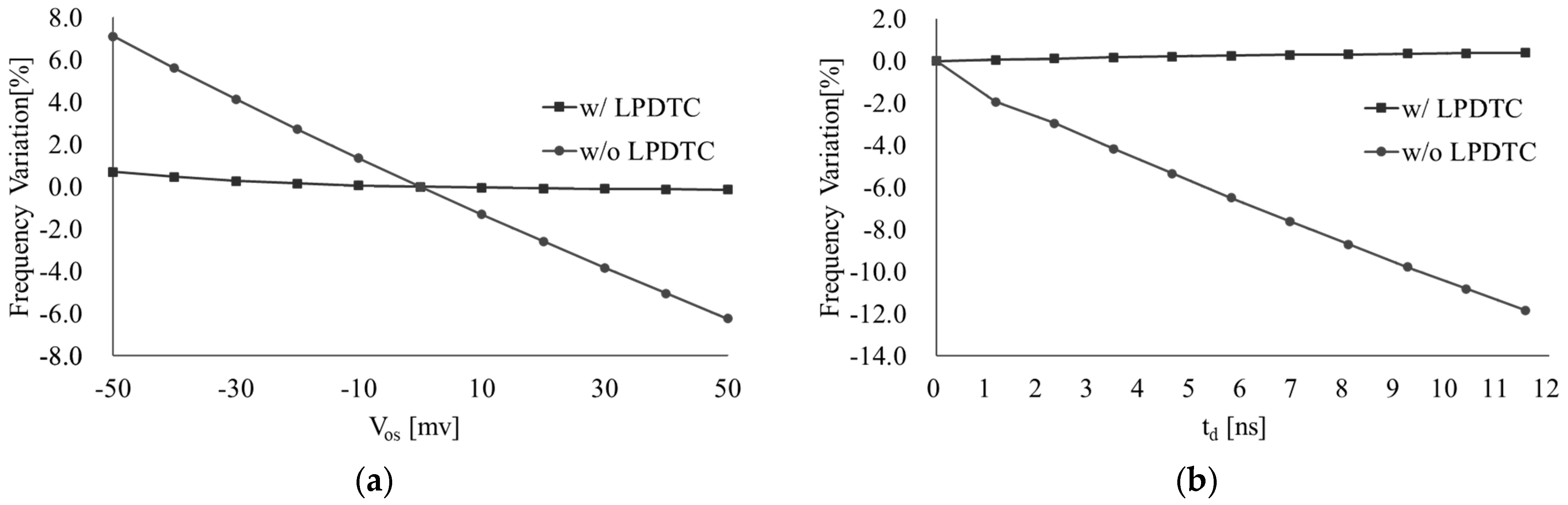
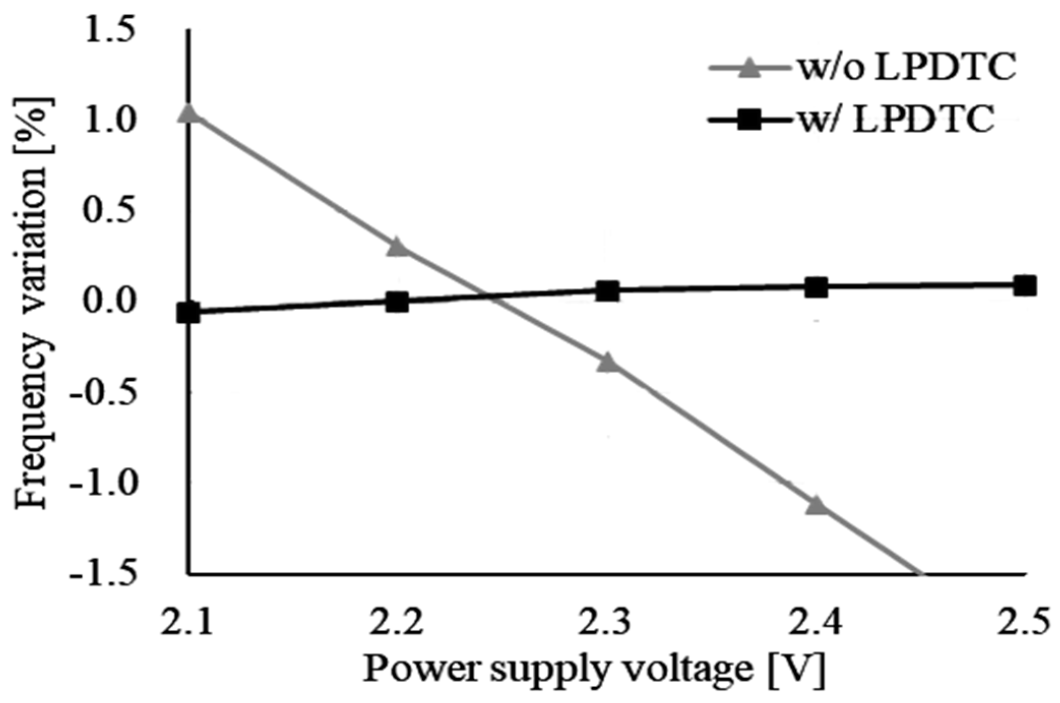
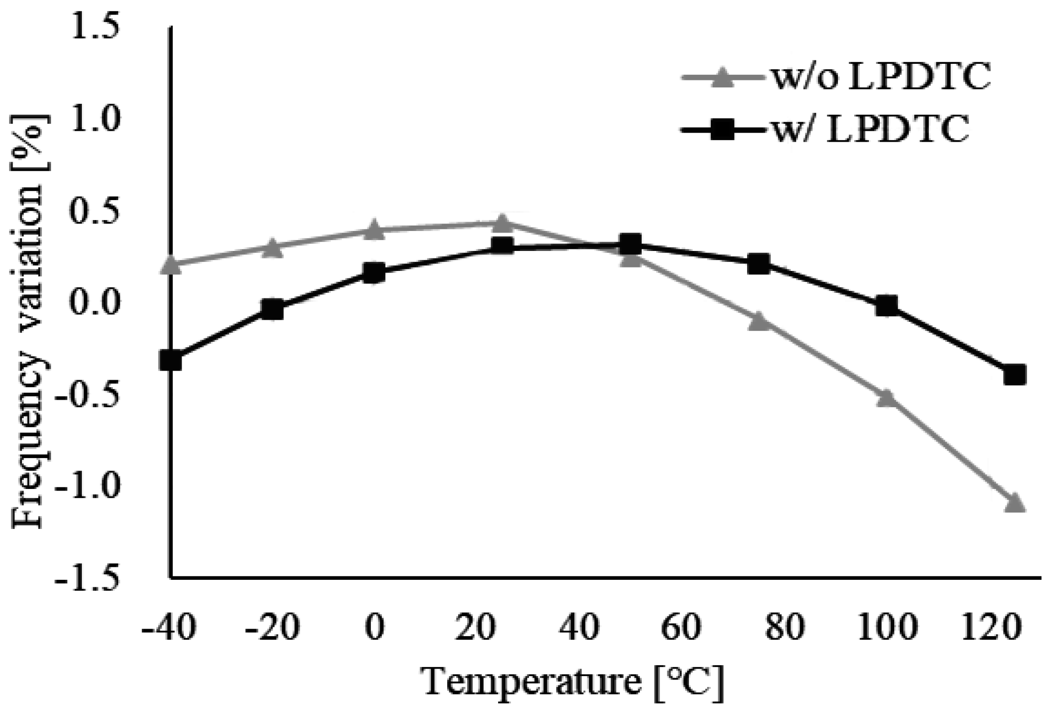
Low-power delay time cancellation (LPDTC) technique: This innovative technique minimizes the impact of the comparator delay time and offsets voltage while maintaining low current consumption by utilizing only two comparators.
(2)
Current ratio adjustment (CRA) method: This method mitigates temperature-induced variations in resistors by adjusting the ratio of the reference currents in the relaxation oscillators.

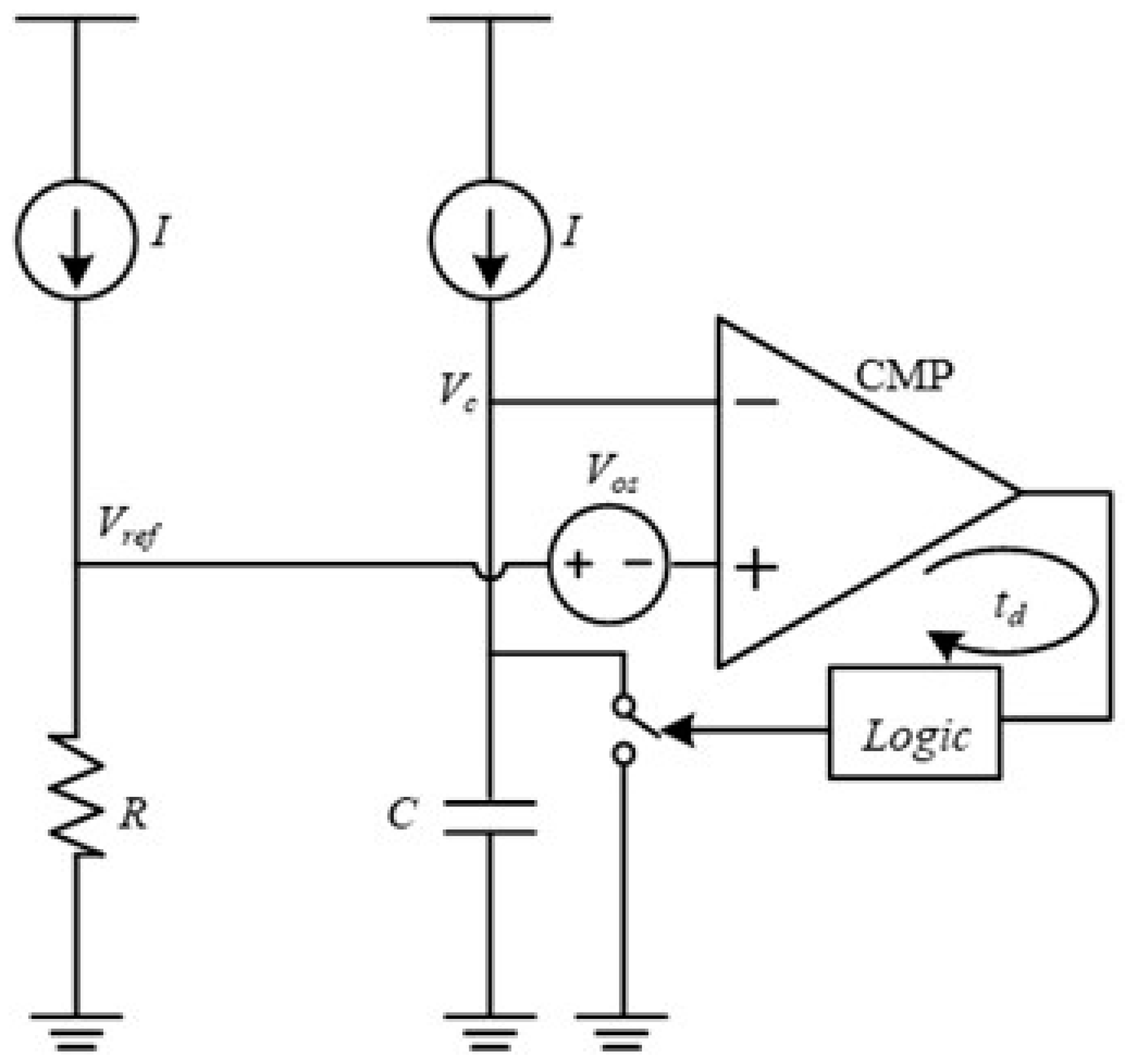
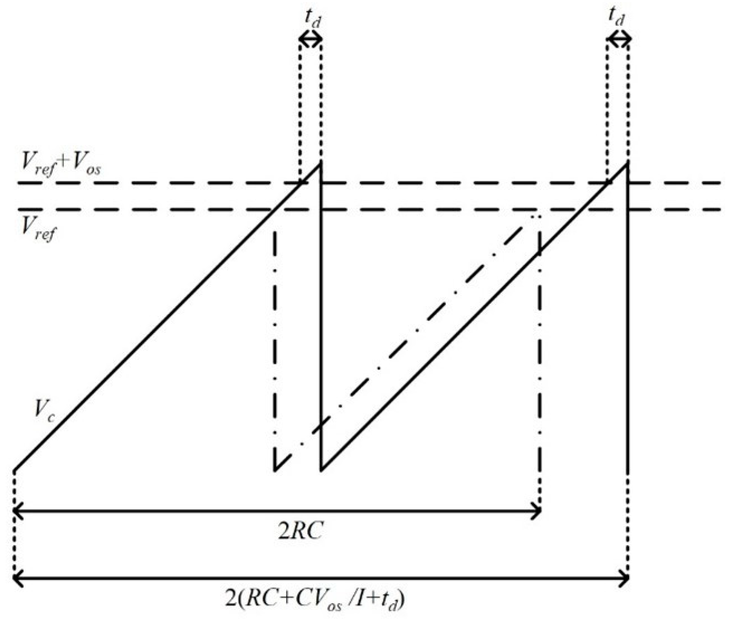
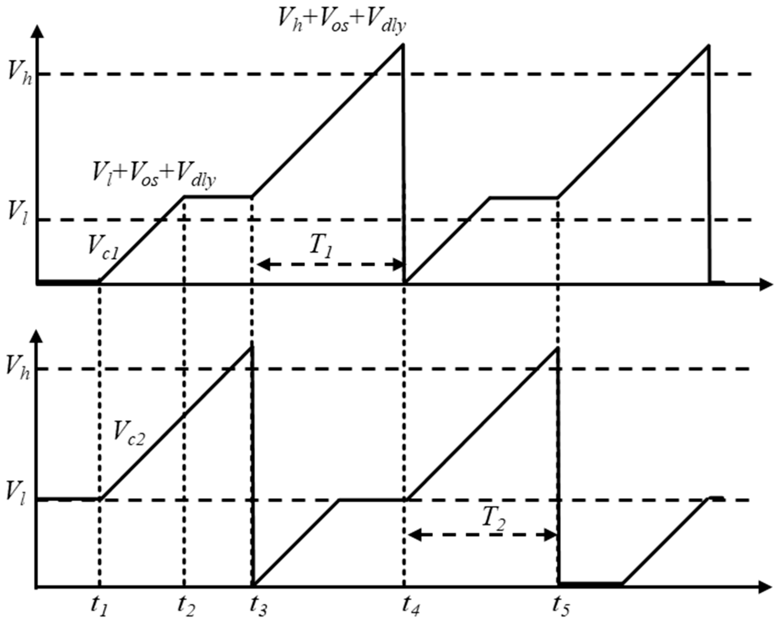
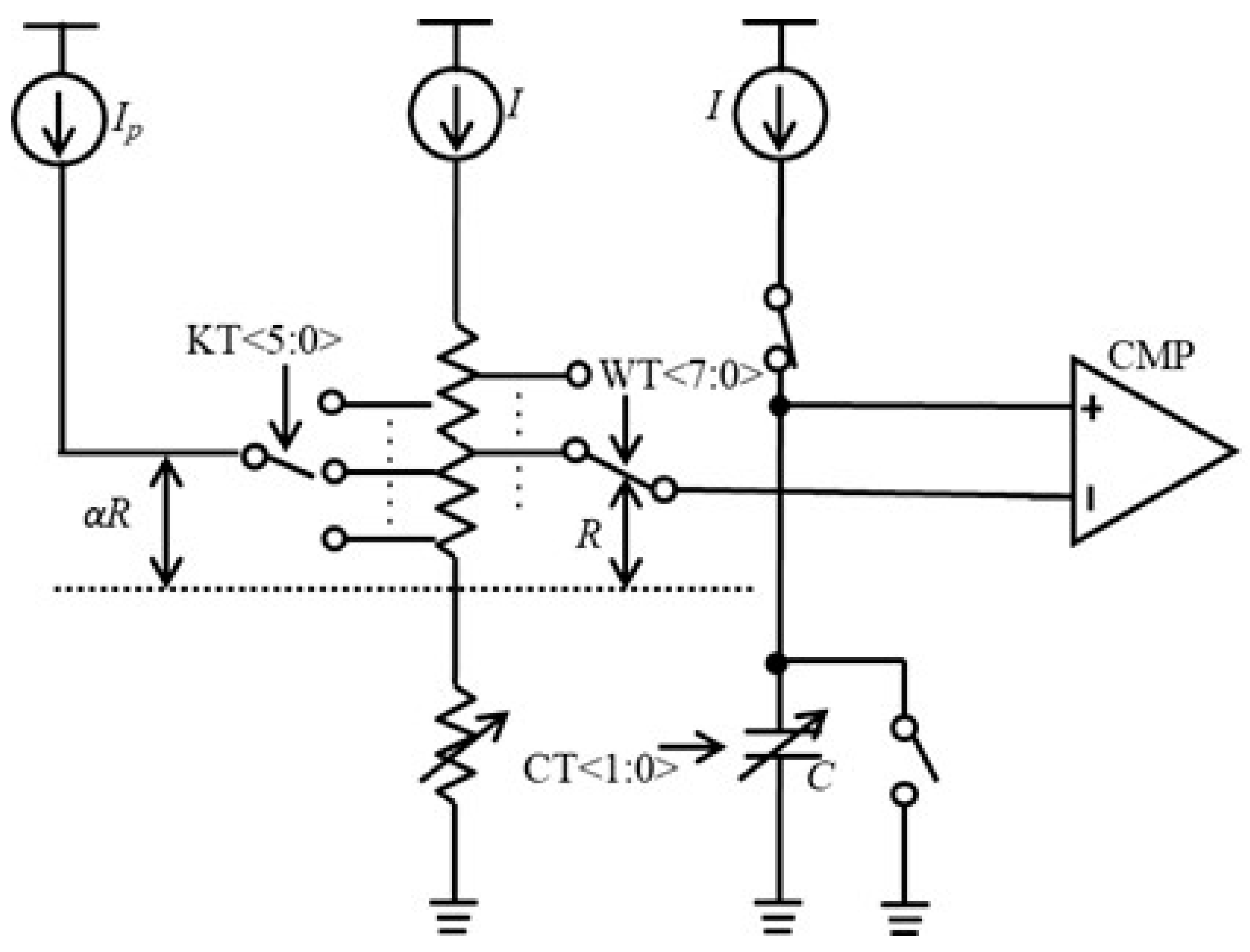
2. Delay Time Cancellation Technique

The basic structure of a conventional relaxation oscillator is shown in Figure 1. The period (Tosc) is typically determined by the RC time constant. However, Tosc is affected by the comparator offset voltage (Vos) and delay time (td). As illustrated in Figure 2, the reference voltage deviates from its original reference (Vref) due to the influence of Vos. The comparator cannot react in a timely manner when the comparison voltage (Vc) reaches the reference voltage (Vref + Vos), resulting in a delay time td. Hence, the equation describing the oscillator period becomes Tosc = 2(RC + CVos/I + td), where I is the bias current. Vos and td are easily affected by PVT variations, which leads to the instability of the clock period.
To eliminate the impact of comparator delay time and offset voltage, the LPDTC technique is proposed and implemented in the relaxation oscillator (Figure 3). The principle of the LPDTC technique can be illustrated in Figure 4. In the first charging phase, from t1 to t2, Vref1 is equal to Vl, and the capacitor C1 is charged until VC1 reaches Vl + Vos + Vdly by current I shown in Figure 3 (where Vdly = Itd/C1). Subsequently, before further charging to Vh + Vos + Vdly, a brief waiting period is required from t2 to t3. Following this, the second charging phase of C1 occurs from t3 to t4, with a certain duration
T 1 = ( V h + V o s + V d l y ) ( V l + V o s + V d l y ) k = ( V h V l ) k
where k represents the slew rate, equal to C1/I. Since C2 experiences the same charge process as C1, we can get T2 = t5t4 = T1 in the condition of C1 = C2 = C. Therefore, the clock period of the proposed oscillator is
T o s c = 1 f 0 = 2 T 1 = 2 C ( V h V l ) I = 2 R C
As shown in Equation (2), Tosc is not affected by Vos and td. Thus, the proposed LPDTC technique can improve the frequency variation of the oscillator caused by changes in Vos and td.
It is important to note that while capacitor leakage currents and charge injection effects from MOS switches, such as S1a and S1b, can potentially influence the clock period, their impact is minimized in this study. To address these issues, we employ Metal–Organic–Metal (MOM) capacitors to significantly reduce leakage currents. Furthermore, capacitors C1 and C2 are sized approximately 100 times larger than the parasitic capacitance of the MOS switches, effectively mitigating the charge injection effects. As a result, the influence of these factors on the clock period is minimal.
To achieve the above operation, a specialized control circuit is designed to control the operational status of the proposed oscillator shown in Figure 3. The action waveforms of this circuit are shown in Figure 5. At the beginning of one period, the signal S4a is set high to make Vref2 equal to Vh. When the rising edge of Clkb_d occurs, Vref2 falls to Vl because S4a is set low. Meanwhile, S2a is changed to high to start the first charging phase of the capacitor C2. In this phase, the comparator delay time is converted to voltage and stored. After Vc2 exceeds Vref2, Cmp2o is triggered, making S2a change to low and S4a to high. Under this condition, the charging of capacitor C2 stops, and Vc2 is held. When the rising edge of Clk occurs, the capacitor C2 is charged again by controlling S2a. As described in Equation (1), the time for this charging phase is not affected by comparator delay. The action waveforms of the circuit surrounding CMP1 exhibit a 180-degree phase difference, similar to those shown in Figure 5. These periodic actions enable the clock signal to output continuously, remaining unaffected by the comparator delay time and offset voltage.
The optimization of charging circuits is necessary for the relaxation oscillator using the LPDTC technique. Figure 6a illustrates the conventional structure of a charging circuit. During the holding phase, the current I becomes zero (as shown in Figure 7a) because MP1 enters the linear region when S1a is at a low level. When S1a transitions back to a high level, the current I needs time to recover, resulting in a variation in Vc1. Additionally, the resistance of switches MN1, MN2, and MN3 in the variable capacitor impacts the charging time. To address these issues, a novel charging circuit is proposed, as shown in Figure 6b. When S1a is at a low level, current I flow to R1, ensuring that MP1 remains in the saturation region. Consequently, the current I remains constant when S1a changes (as shown in Figure 7b). It should be noted that MP2 and MP3 are not controlled by a non-overlap clock due to the impact of the delay of the clock on its frequency. Furthermore, the structure of the variable capacitor is optimized. The resistance of the switches MN1, MN2, and MN3 does not impact the charging time, because the currents flowing through them are zero. For instance, when switches MN5 and MN2 are turned on, capacitor C12 is selected. In this scenario, Vc1 is equal to Vc12 because no current flows through MN2. Furthermore, the resistance of switch MN5 also does not influence the charging time since the sampled voltage is Vc12 rather than the voltage at the drains of the MOS transistors depicted in Figure 6a.
The simulation results illustrating the effects of Vos and td are presented in Figure 8. When Vos varies from −60 mV to 60 mV, the frequency variation of the oscillator using LPDTC is improved to 0.85%, compared to 13.34% without LPDTC. Similarly, with a variation in td of 12 ns, the frequency variation in the oscillator using LPDTC is improved to 0.38%, compared to 12.1% without LPDTC. These simulation results demonstrate the effectiveness of the LPDTC technique in mitigating frequency variation caused by Vos and td.

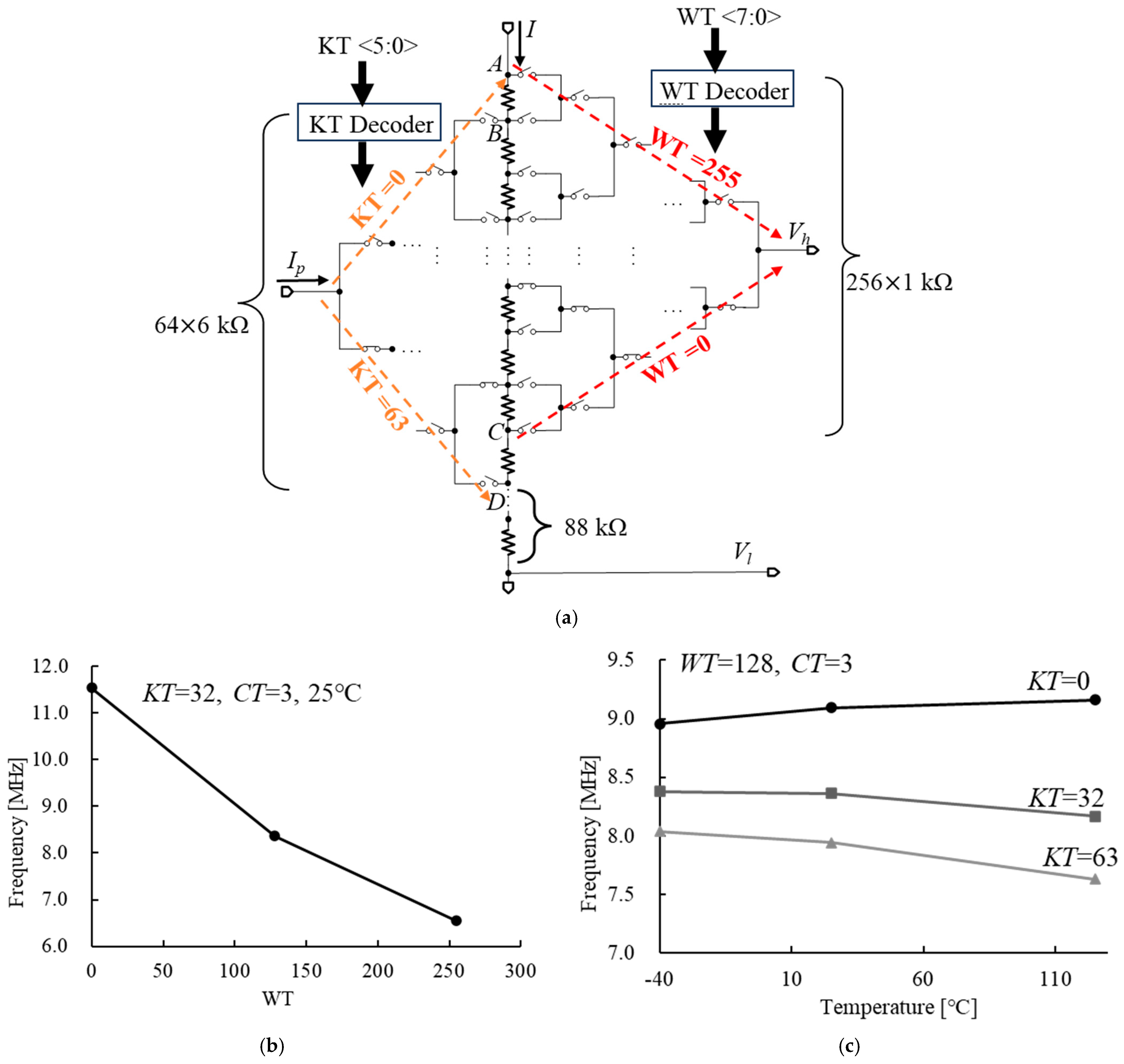
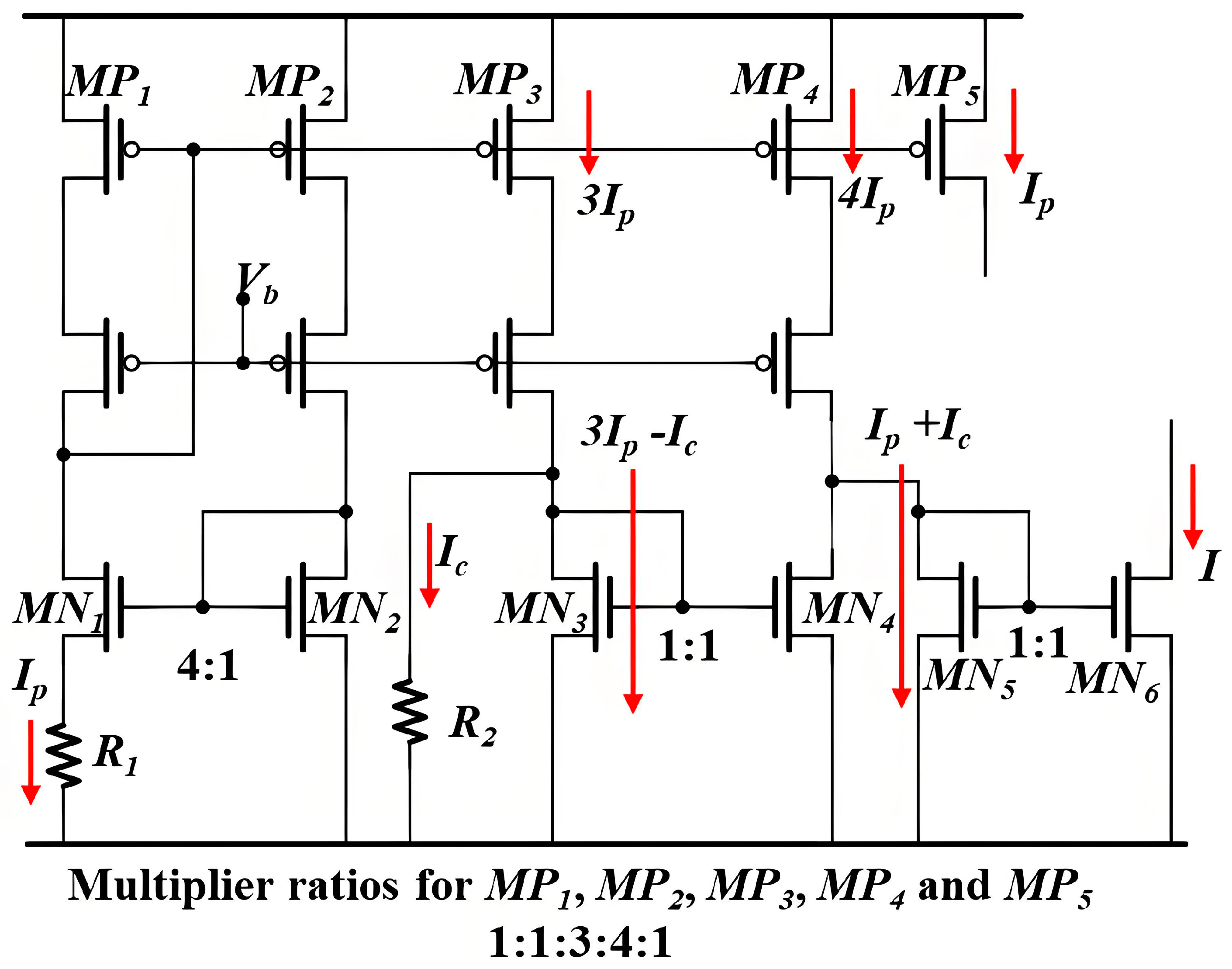
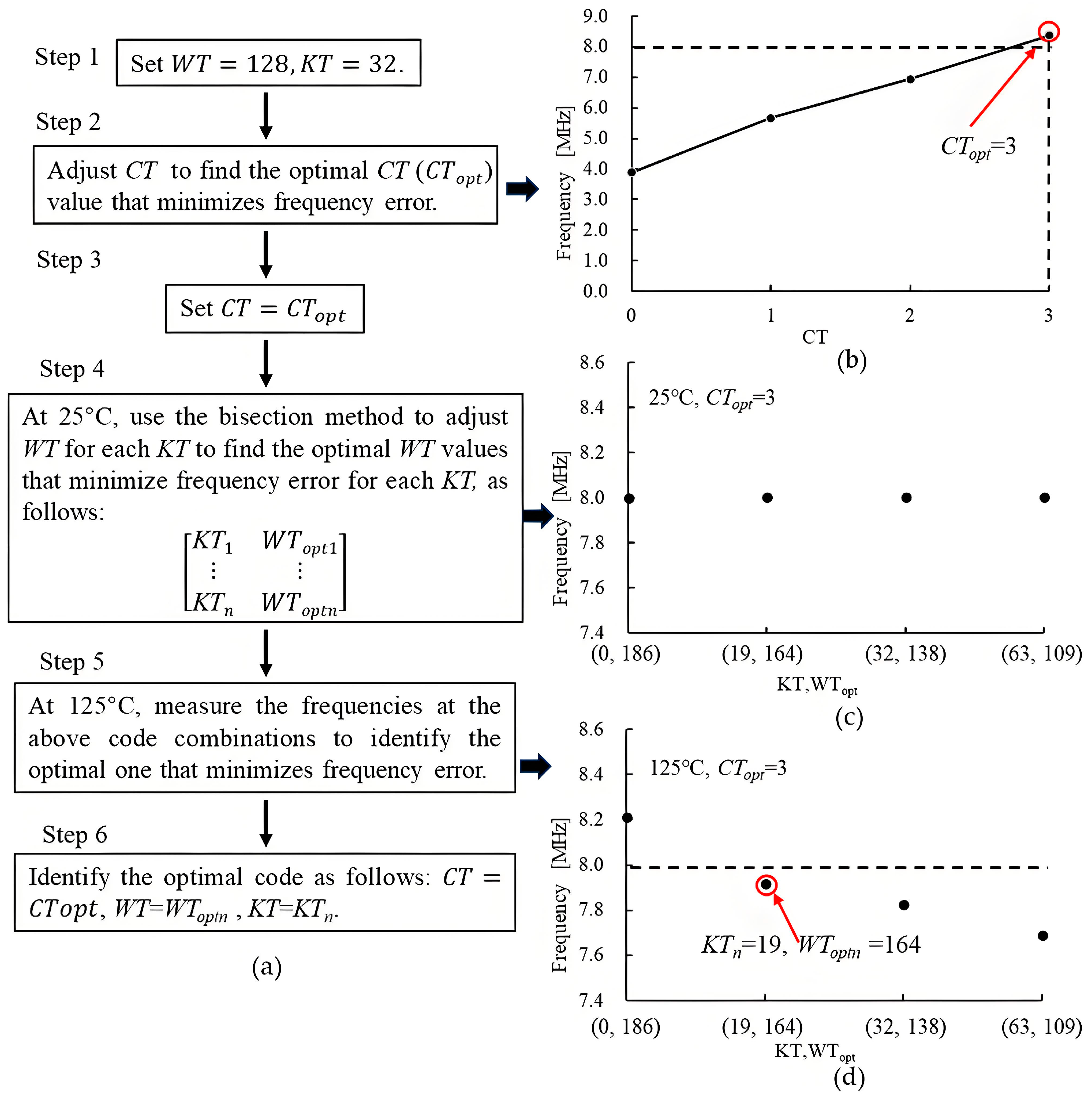
3. Current Ratio Adjustment Method

Implementing temperature compensation in the relaxation oscillator is crucial due to the temperature-induced variations in resistor R, which affect the frequency, as shown in Equation (2). In this work, we propose the current ratio adjustment (CRA) method to compensate for these variations by adjusting the current ratio, as illustrated in Figure 9. This approach contrasts with the temperature coefficient adjustment of reference currents employed in certain bandgap reference (BGR) circuits [25,26]. In those BGR circuits, the adjustment of the temperature coefficient of the reference current is achieved by modifying the values of resistors that determine the reference current through MOS switches. However, since these MOS switches are connected in series or parallel with the resistors, their resistance can impact the temperature coefficient of the reference currents. Consequently, the size of these MOS switches must be sufficiently large to mitigate this influence, which in turn increases the overall size of the circuit. In contrast, our proposed CRA method does not involve altering the reference current itself, providing an advantage by effectively mitigating the impact of the resistance of the MOS switches on both the reference current and the overall circuit size. The proposed circuit introduces a positive temperature coefficient of absolute temperature (PTAT) current [25,26,27,28,29], Ip. The frequency of the oscillator can be expressed as
f 0 = 1 2 R C I I + α I p
where α is the resistance ratio shown in Figure 9. Assuming I is a temperature-insensitive current and all higher-order (≥2) temperature coefficients are zero, we have
f 0 = 1 2 R C I I + α I p = I 2 R 0 C ( 1 + λ R Δ T ) [ I + α I p 0 ( 1 + λ I p Δ T ) ] = I 2 R 0 C ( I + α I p 0 ) I 1 + Δ T ( λ R + λ I p I r a t i o + 1 )
where Iratio is equal to I/αIp0; R0 and Ip0 are the values of R and Ip at room temperature, respectively; and λR and λIp are the first-order temperature coefficients (TC1) of R and Ip, respectively. It can be obtained from Equation (4) that when Iratio satisfies Equation (5), f0 becomes insensitive to temperature.
I r a t i o = - ( λ I p λ R + 1 )
As depicted in Figure 9, we can adjust α by modifying the 6-bit temperature coefficient control word KT, thereby adjusting Iratio. The circuit involving the variable resistor R is illustrated in Figure 10a. The switches are controlled by KT and WT through their respective decoders. When KT is set to zero, Ip flows through node B. Conversely, when KT is set to 63, Ip flows through node D. Additionally, when WT is set to 255, the voltage Vh corresponds to the voltage at node A. In contrast, when WT is set to zero, Vh reflects the voltage at node C. The example results obtained from varying the values of WT and KT are illustrated in Figure 10b and Figure 10c, respectively.
From Figure 10, we can calculate
α = 88 + 6 K T 280 + W T
where WT is the 8-bit control word used to adjust the absolute frequency of the oscillator.
The currents I and Ip are provided by the proposed reference current generator depicted in Figure 11. Since MN1 and MN2 operate in the subthreshold region, Ip can be expressed as
I p = ζ R 1 k T q ln n
where ζ, k, and q are the subthreshold slope factor, Boltzmann constant, and elementary charge, respectively. Then, I can be expressed as
I = I p + I c = ζ R 1 k T q ln n + V G S 2 R 2
Given that MN3 also operates in the subthreshold region, Ic is a complementary-to-absolute-temperature (CTAT) current. Consequently, the temperature-insensitive current I can be achieved.
Figure 12 illustrates the simulation results of Ip, Ic, and I as functions of temperature, confirming that their temperature characteristics align with the theoretical predictions.
The adjustable range of λIp/(Iratio + 1) is presented in Figure 13. This range can accommodate the TC1 of the resistor R with a margin exceeding ±100 ppm/°C across all MOSFET corners. This implies that a temperature-insensitive oscillation frequency can be obtained at each MOSFET corner by adjusting the control word KT.
The frequency trimming process is illustrated in Figure 14a. Initially, WT and KT are set to 128 and 32, respectively. Next, CT (the control words of the variable capacitor shown in Figure 6a) is adjusted to find the optimal value (CTopt) that minimizes frequency error. Figure 14b presents an example of the results obtained from this step. Then, CT is set to CTopt, and WT is adjusted using the bisection method for each KT to find the optimal WT values that minimize frequency error for each KT at 25 °C, as follows:
K T 1 W T o p t 1 K T n W T o p t n
Figure 14c presents an example of the results obtained from this step.
Subsequently, at 125 °C, the frequencies for the above code combinations are measured to identify the optimal one that minimizes frequency error. Figure 14c presents an example of the results obtained from this step. Finally, the optimal code is identified as CT = CTopt, WT = WToptn, and KT = KTn. The trimming resolution of WT is approximately 0.15%, and that of KT is 6.25 ppm/°C. Therefore, the trimming error is about 0.13% across the temperature range from −40 °C to 125 °C.

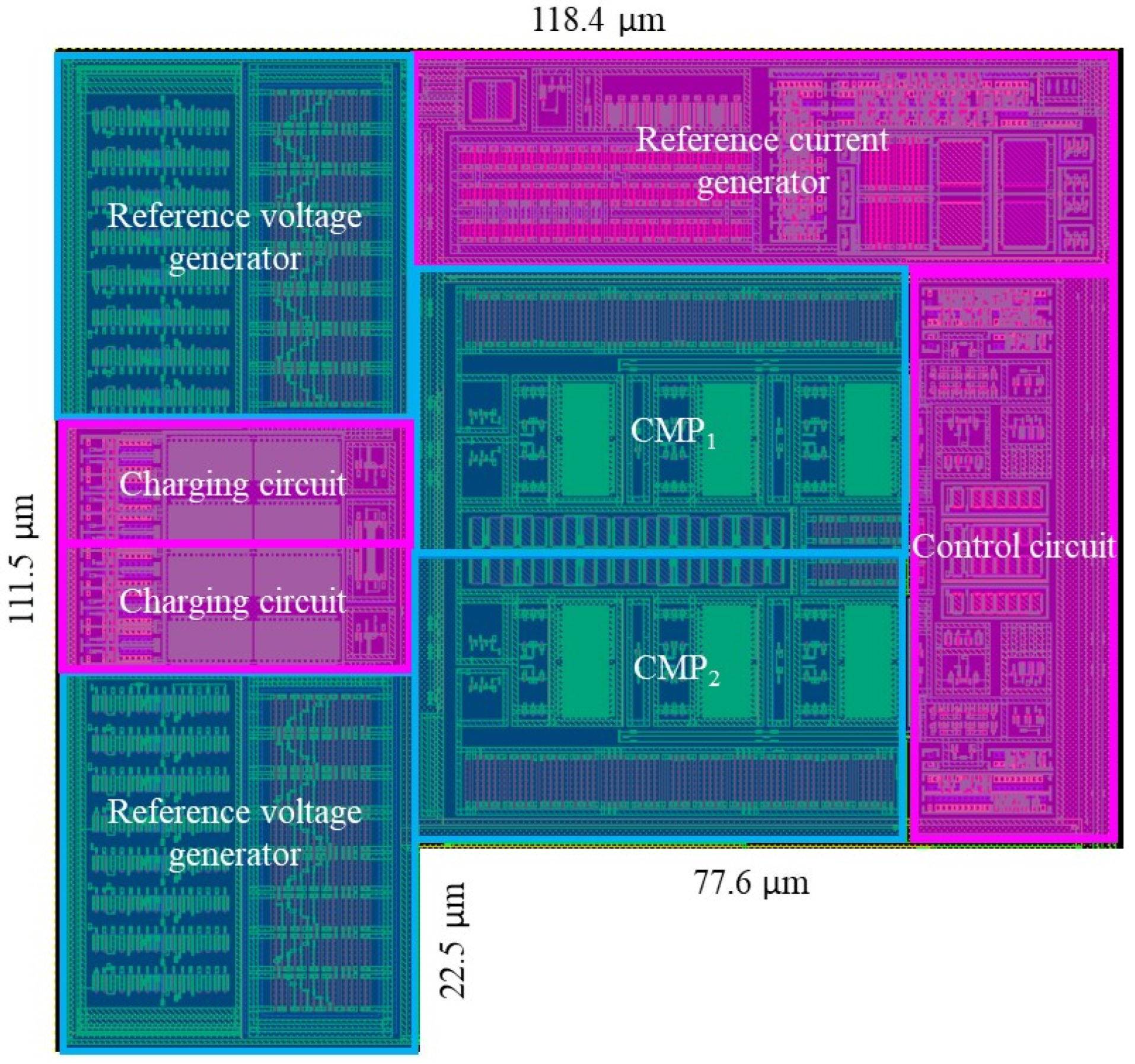
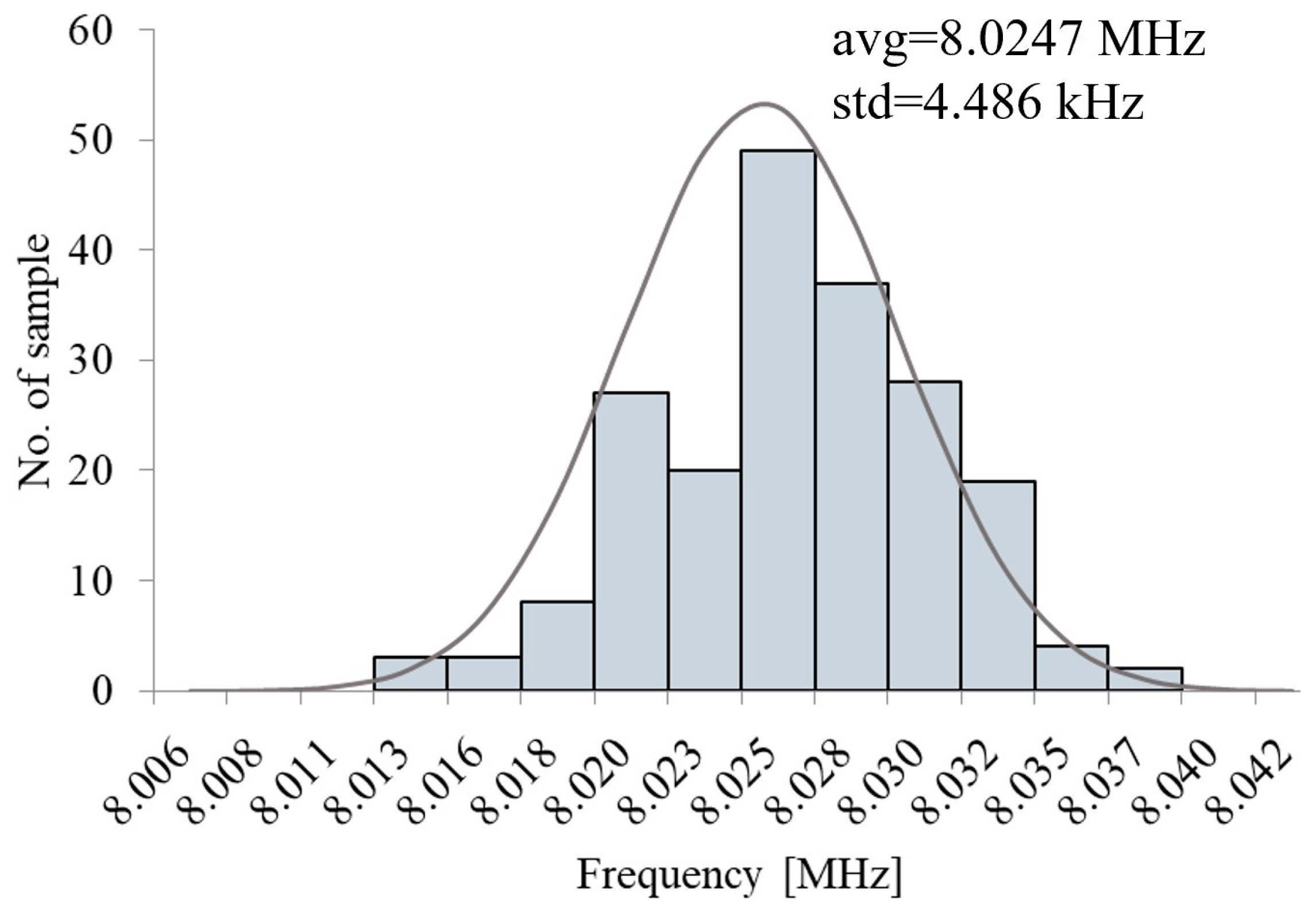
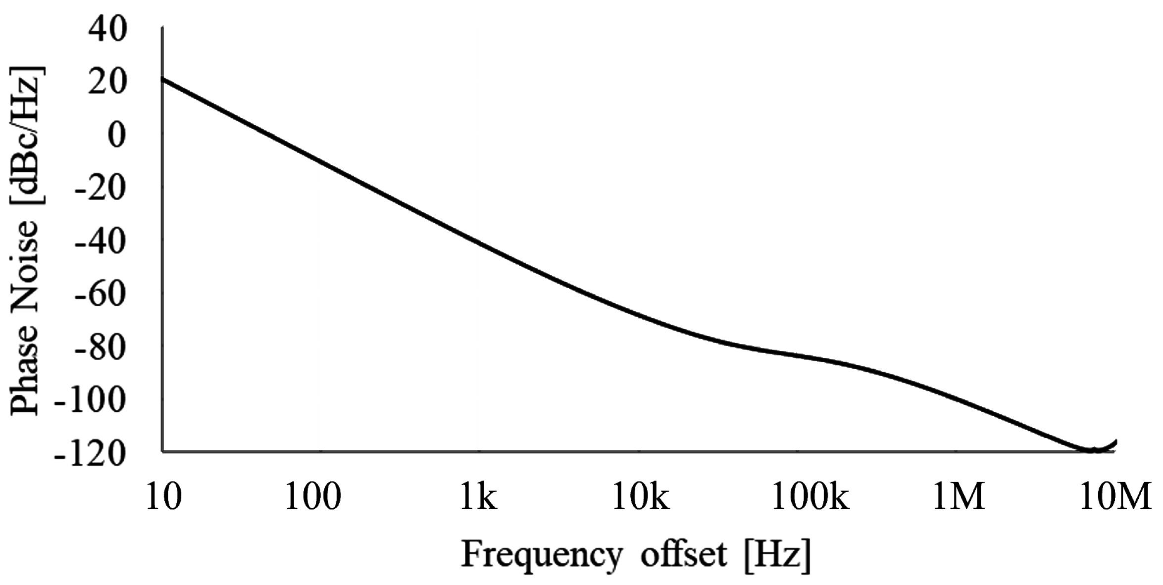
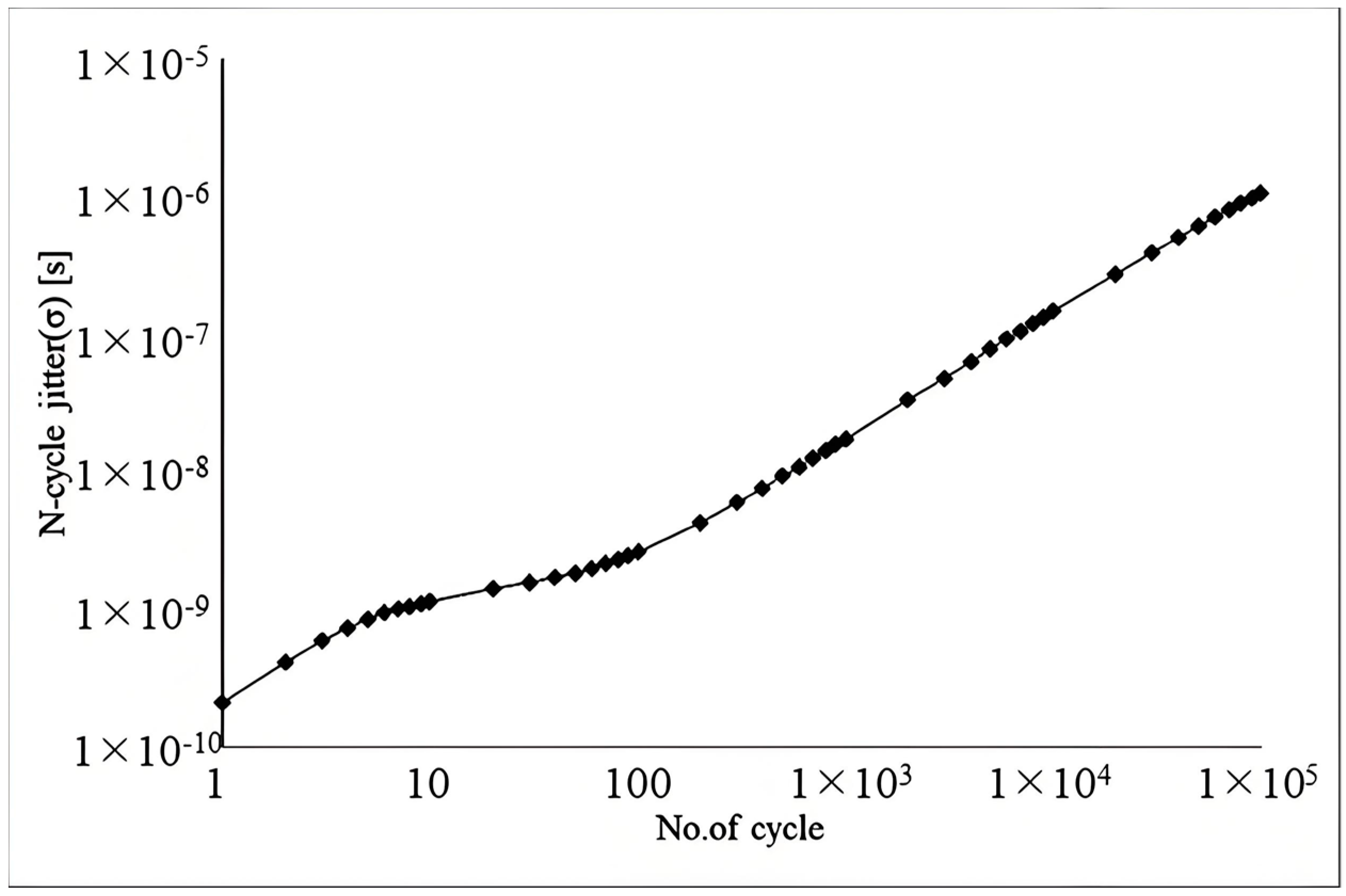
4. Simulation Results

The proposed LPDTC technique and CRA method are implemented in an 8 MHz relaxation oscillator designed using a 40 nm CMOS process. Figure 15 shows the layout of the proposed oscillator.
Figure 16 displays the waveforms following the reset of the oscillator. It is evident that by the second clock cycle post-reset, the control circuit functions as shown in Figure 5, resulting in a stabilized clock period. The frequency standard deviation is 4.486 kHz, as shown by the 200-point Monte Carlo simulation result in Figure 17. The phase noise results presented in Figure 18 have been obtained through Periodic Steady-State (PSS) and Phase Noise (Pnoise) simulations. The N-cycle jitter σ N j illustrated in Figure 19 can be calculated by integrating the phase noise, as described in Equation (10)
σ N j = 2 π f 0 · 100 Hz 1 GHz L ( Δ f ) · sin 2 ( π Δ f · N f 0 )
where L ( Δ f ) represents the phase noise of the oscillator at a frequency offset Δf, and N denotes the number of cycles. Figure 20 demonstrates that with the LPDTC technique, the frequency variation due to power supply voltage fluctuations is improved to approximately 0.15%, compared to over 2% without it. Furthermore, Figure 21 illustrates that after the temperature compensation using the CRA method, the frequency variation due to temperature changes is reduced to approximately ±0.4% with the LPDTC technique, compared to ±0.8% without it. Although the second-order temperature dependence observed in Figure 21 is a result of neglecting all higher-order temperature coefficients in the CRA method, as indicated in Equation (4), the frequency variation due to temperature changes remains sufficiently small for most applications of relaxation oscillators. The performance comparison with other designs is presented in Table 1, which shows that the proposed oscillator can operate at a higher frequency with low frequency variation and low current consumption.

5. Conclusions

This paper presents an innovative LPDTC technique and a CRA method, which effectively mitigate comparator delay time, offset voltage and temperature-induced variations in resistors. These methods are implemented in an 8 MHz relaxation oscillator designed using a 40 nm CMOS process. As a result, the oscillator achieves a line sensitivity of 0.38%/V and a temperature sensitivity of 43 ppm/°C over a temperature range of −40 °C to 125 °C.

Author Contributions

Conceptualization, K.X. and G.Z.; methodology, Z.H.; software, H.D. and Z.W.; validation, Z.H., Z.W. and H.D.; formal analysis, K.X.; investigation, K.X.; resources, G.Z.; data curation, Z.H. and K.X.; writing—original draft preparation, Z.H.; writing—review and editing, Z.H., K.X., H.D., Z.H., X.Y. and G.Z.; visualization, Z.H., K.X., H.D. and Z.W.; supervision, X.Y. and G.Z.; project administration, G.Z.; funding acquisition, G.Z. All authors have read and agreed to the published version of the manuscript.

Funding

This research received no external funding.

Data Availability Statement

The original contributions presented in this study are included in the article. Further inquiries can be directed to the corresponding author.

Conflicts of Interest

Authors Kunpeng Xu, Hongguang Dai, Zhanxia Wu were employed by the company Beijing Smartchip Microelectronics Technology Co., Ltd. The remaining authors declare that the research was conducted in the absence of any commercial or financial relationships that could be construed as a potential conflict of interest.

References

  1. Hao, H.; Dai, F. Design of smart home security system based on 52 MCU. J. Adv. Artif. Life Robot. 2021, 1, 199–203. [Google Scholar]
  2. Otani, S.; Kondo, H. RX v2: Renesas’s new-generation MCU processor. IEICE Trans. Electron. 2015, 98, 544–549. [Google Scholar] [CrossRef]
  3. Kawamura, Y.; Okada, N.; Matsuda, Y.; Matsumura, T.; Makino, H.; Arimoto, K. A Field Programmable Sequencer and Memory with Middle Grained Programmability Optimized for MCU Peripherals. IEICE Trans. Fundam. Electron. Commun. Comput. Sci. 2016, 99, 917–928. [Google Scholar] [CrossRef]
  4. Takashi, K.; Taito, Y.; Hidaka, H. Essential Roles, Challenges and Development of Embedded MCU Micro-Systems to Innovate Edge Computing for the IoT/AI Age. IEICE Trans. Electron. 2020, 103, 132–143. [Google Scholar]
  5. Liu, Y.; Zhu, Z.; Bao, R.; Yang, S.; Liu, J.; Zhou, X.; Li, Q. A Low-Power RC Oscillator with Offset and Path Delay Cancellation. In Proceedings of the 2021 IEEE International Conference on Integrated Circuits, Technologies and Applications, Zhuhai, China, 24–26 November 2021. [Google Scholar]
  6. Chang, Y.-A.; Adiono, T.; Hamidah, A.; Liu, S.-I. An on-chip relaxation oscillator with comparator delay compensation. IEEE Trans. Very Large Scale Integr. (VLSI) Syst. 2019, 27, 969–973. [Google Scholar] [CrossRef]
  7. Hsiao, K. A 32.4 ppm/°C 3.2-1.6 V self-chopped relaxation oscillator with adaptive supply generation. In Proceedings of the 2012 Symposium on VLSI Circuits, Honolulu, HI, USA, 13–15 June 2012. [Google Scholar]
  8. Truesdell, D.S.; Li, S.; Calhoun, B.H. A 0.5V 560kHz 18.8fJ/Cycle Ultra-Low Energy Oscillator in 65nm CMOS with 96.1ppm/°C Stability using a Duty-Cycled Digital Frequency-Locked Loop. In Proceedings of the 2020 IEEE Symposium on VLSI Circuits, Honolulu, HI, USA, 16–19 June 2020. [Google Scholar]
  9. Wang, J.; Goh, W.L. A 13.5-MHz relaxation oscillator with ±0.5% temperature stability for RFID application. In Proceedings of the 2016 IEEE International Symposium on Circuits and Systems, Montreal, QC, Canada, 22–25 May 2016. [Google Scholar]
  10. Cao, Y.; Leroux, P.; De Cock, W.; Steyaert, M. A 63,000 Q-factor relaxation oscillator with switched-capacitor integrated error feedback. In Proceedings of the 2013 IEEE International Solid-State Circuits Conference Digest of Technical Papers, San Francisco, CA, USA, 17–21 February 2013. [Google Scholar]
  11. Paidimarri, A.; Griffith, D.; Wang, A.; Burra, G.; Chandrakasan, A.P. An RC Oscillator with Comparator Offset Cancellation. IEEE J. Solid-State Circuits 2016, 51, 1866–1877. [Google Scholar] [CrossRef]
  12. Chiang, Y.-H.; Liu, S.-I. A Submicrowatt 1.1-MHz CMOS Relaxation Oscillator with Temperature Compensation. IEEE Trans. Circuits Syst. II Express Briefs 2013, 60, 837–841. [Google Scholar] [CrossRef]
  13. Lee, J.; George, A.K.; Je, M. An ultra-low-noise swing-boosted differential relaxation oscillator in 0.18-µm CMOS. IEEE J. Solid-State Circuits 2020, 55, 2489. [Google Scholar] [CrossRef]
  14. Sun, J.; Hana, Y. A low power low supply sensitivity current-mode relaxation oscillator. IEICE Electron. Express 2014, 11, 23. [Google Scholar] [CrossRef]
  15. Li, Z.; Li, Z.; Zhao, H.; Zhao, H.; Yin, J.; Yin, J.; Qiao, S.; Qiao, S.; Zhou, Y.; Zhou, Y. A fully integrated RC oscillator with adaptive-body-biasing. IEICE Electron. Express 2022, 19, 20220102. [Google Scholar] [CrossRef]
  16. Xie, Z.; Zou, Z.; Lv, Z.; Yi, Y.; Zhang, J.; Tong, Q.; Liu, D. A 2.9 MHz low power RC relaxation oscillator with delay equivalent electric charges storage and fully covered trimming strategy. Microelectron. J. 2024, 143, 106062. [Google Scholar]
  17. Hu, Y.; Li, Z.; Hou, J.; Ma, W.; Lu, C.; Xiao, Z.; Liu, H.; Hu, W. A constant charging-current relaxation oscillator with a duty-cycled main comparator and an adaptive auxiliary comparator. Microelectron. J. 2022, 128, 105566. [Google Scholar]
  18. Mikulić, J.; Schatzberger, G.; Barić, A. A 1-MHz on-chip relaxation oscillator with comparator delay cancelation. In Proceedings of the 2017 43rd IEEE European Solid State Circuits Conference (ESSCIRC), Leuven, Belgium, 11–14 September 2017. [Google Scholar]
  19. Ge, R.; Chen, C.; Jiang, D. A Digitally Controlled Output Adjustable High Stability Relaxation Oscillator. In Proceedings of the 2024 36th Chinese Control and Decision Conference, Xi’an, China, 25–27 May 2024. [Google Scholar]
  20. Lee, J.; Cho, S. A 10MHz 80μW 67 ppm/°C CMOS reference clock oscillator with a temperature compensated feedback loop in 0.18μm CMOS. In Proceedings of the 2009 Symposium on VLSI Circuits, Kyoto, Japan, 16–18 June 2009. [Google Scholar]
  21. Jang, T.; Choi, M.; Jeong, S.; Bang, S.; Sylvester, D.; Blaauw, D. A 4.7nW 13.8ppm/°C self-biased wakeup timer using a switched-resistor scheme. In Proceedings of the 2016 IEEE International Solid-State Circuits Conference, San Francisco, CA, USA, 31 January–4 February 2016. [Google Scholar]
  22. Zhou, R.; Wang, L.; Yang, J.; Li, Z.; Zhao, X.; Liu, S. A 8.1-nW, 4.22-kHz, −40–85 °C relaxation oscillator with subthreshold leakage current compensation and forward body bias buffer for low power IoT applications. Microelectron. J. 2024, 144, 106090. [Google Scholar] [CrossRef]
  23. Gürleyük, Ç.; Pedalà, L.; Pan, S.; Sebastiano, F.; Makinwa, K.A.A. A CMOS Dual-RC Frequency Reference with ±200-ppm Inaccuracy from −45 °C to 85 °C. IEEE J. Solid-State Circuits 2018, 53, 3386–3395. [Google Scholar]
  24. Gürleyük, Ç.; Pan, S.; Makinwa, K.A.A. A 16MHz CMOS RC Frequency Reference with ±400ppm Inaccuracy from −45°C to 85°C After Digital Linear Temperature Compensation. IEEE J. Solid-State Circuits 2020, 53, 64–66. [Google Scholar]
  25. Ge, G.; Zhang, C.; Hoogzaad, G.; Makinwa, K.A.A. A Single-Trim CMOS Bandgap Reference with a 3σ Inaccuracy of ± 0.15% from −40 °C to 125 °C. IEEE J. Solid-State Circuits 2011, 46, 2693–2701. [Google Scholar]
  26. Lee, T.-J.; Tu, K.-H. High-Sensitivity PTAT Current Generator Using PTAT and CTAT Current Subtraction Method for Temperature Sensor with Frequency Output. IEEE Trans. Circuits Syst. II Express Briefs 2023, 70, 3922–3926. [Google Scholar]
  27. Amaravati, A.; Dave, M.; Baghini, M.S.; Sharma, D.K. 800-nA Process-and-Voltage-Invariant 106-dB PSRR PTAT Current Reference. IEEE Trans. Circuits Syst. II Express Briefs 2013, 60, 577–581. [Google Scholar]
  28. Sabharwal, S.; Kaur, J.; Shahi, A. Various Current Mirror Topologies: A Survey. In Proceedings of the 2022 2nd International Conference on Advance Computing and Innovative Technologies in Engineering, Greater Noida, India, 28–29 April 2022. [Google Scholar]
  29. Bonteanu, G.; Cracan, A. A high-gain programmable current mirror for large bias currents generation. In Proceedings of the 2017 5th International Symposium on Electrical and Electronics Engineering, Galati, Romania, 20–22 October 2017. [Google Scholar]
  30. Huang, K.-K.; Wentzloff, D.D. A 1.2-MHz 5.8-μW Temperature-Compensated Relaxation Oscillator in 130-nm CMOS. IEEE Trans. Circuits Syst. II Express Briefs 2014, 61, 334–338. [Google Scholar]
  31. Zhou, W.; Goh, W.L.; Gao, Y. A 3-MHz 17.3-μW 0.015% Period Jitter Relaxation Oscillator with Energy Efficient Swing Boosting. IEEE Trans. Circuits Syst. II Express Briefs 2020, 67, 1745–1749. [Google Scholar]
  32. Lei, K.-M.; Mak, P.-I.; Martins, R.P. A 0.35-V 5,200-μm2 2.1-MHz Temperature-Resilient Relaxation Oscillator with 667 fJ/Cycle Energy Efficiency Using an Asymmetric Swing-Boosted RC Network and a Dual-Path Comparator. IEEE J. Solid-State Circuits 2021, 56, 2701–2710. [Google Scholar]
  33. Choe, K.; Bernal, O.D.; Nuttman, D.; Je, M. A precision relaxation oscillator with a self-clocked offset-cancellation scheme for implantable biomedical SoCs. In Proceedings of the 2009 IEEE International Solid-State Circuits Conference-Digest of Technical Papers, San Francisco, CA, USA, 8–12 February 2009. [Google Scholar]
Figure 1. The structure of a conventional relaxation oscillator.
Micromachines 16 00364 g001
Figure 2. The waveform of Vc in the conventional relaxation oscillator.
Micromachines 16 00364 g002
Figure 3. The structure of the relaxation oscillator using the LPDTC technique.
Micromachines 16 00364 g003
Figure 4. The principle of the LPDTC technique.
Micromachines 16 00364 g004
Figure 5. The waveforms of the proposed oscillator.
Micromachines 16 00364 g005
Figure 6. The structure of the charging circuit: (a) conventional structure; (b) proposed structure.
Micromachines 16 00364 g006
Figure 7. The waveforms of the charging current (a) in the conventional charging circuit, and (b) in the proposed charging circuit.
Micromachines 16 00364 g007
Figure 8. The variation in the frequency (a) with the change in Vos and (b) td.
Micromachines 16 00364 g008
Figure 9. Proposed CRA circuit.
Micromachines 16 00364 g009
Figure 10. (a) The structure of the variable resistor R, (b) the example results of adjusting WT, and (c) the example results of adjusting KT.
Micromachines 16 00364 g010
Figure 11. Proposed reference current generator.
Micromachines 16 00364 g011
Figure 12. Simulation results of Ip, Ic, and I.
Micromachines 16 00364 g012
Figure 13. Adjustable range of λIp/(Iratio + 1).
Micromachines 16 00364 g013
Figure 14. (a) The frequency trimming process of the proposed oscillator, and the example results of (b) Step 2, (c) Step 4, and (d) Step 5.
Micromachines 16 00364 g014
Figure 15. The layout of the oscillator.
Micromachines 16 00364 g015
Figure 16. The simulated waveforms following the reset of the oscillator.
Micromachines 16 00364 g016
Figure 17. The Monte Carlo simulation result of the oscillator.
Micromachines 16 00364 g017
Figure 18. The phase noise simulation result of the oscillator.
Micromachines 16 00364 g018
Figure 19. The N-cycle jitter simulation result of the oscillator.
Micromachines 16 00364 g019
Figure 20. Frequency variation due to power supply fluctuations.
Micromachines 16 00364 g020
Figure 21. Frequency variation due to temperature fluctuations.
Micromachines 16 00364 g021
Table 1. Performance comparison with other designs.
Reference[11][12][14][15][16][17][18][22]
Process [nm]651801805518050035065
Supply Voltage [V]0.95~1.051.2~2.41.0~2.00.6~1.11.15~1.253~5.53~4.50.35~0.8
Temp. Range [°C]−40~90−20~80−40~85−40~125−40~125−55~125−40~125−40~85
Frequency [Hz]18.5 k1.1 M100 k33 k2.9 M1 M1 M4.2 k
Current Eff. [μA/MHz]70.45.49.242.1-63.64.88
Temp. Sen. [ppm/°C]856451584512448114
Line Sen. [%/V]530.40.751.2450.160.285.45
Phase Noise @ 100 kHz
[dBc/Hz]
-−79.48---−115.07--
Period Jitter (σ) [ps]----88.96170--
Allen Floor [ppm]20-------
FoM1 [dB]111.5121.1112.7112.6116.1110.296.8117.1
FoM2 [dB]173.4183.0176.6177.1181.7171.8162.1177.5
FoM3 [dB]-131.0--155.3155.3--
Area [mm2]0.1050.075-0.052--0.040.34
Result TypeMeasuredMeasuredPre-simPost-simPost-simMeasuredMeasuredMeasured
Reference[19][30][31][32][13][33]This Work
Process [nm]110130652818013040
Supply Voltage [V]3.30.99~1.010.95~1.450.35~0.381.4~21.4~1.62.1~2.5
Temp. Range [°C]−40~12540~800~90−20~120−40~12520~60−40~125
Frequency [Hz]10 M1.2 M3 M2.1 M10.5 M3.2 M8 M
Current Eff. [μA/MHz]-4.835.771.8514.958.484.1
Temp. Sen. [ppm/°C]133.3296133158137125343
Line Sen. [%/V]-3.60.626.84.40.40.38
Phase Noise @ 100 kHz
[dBc/Hz]
--−114-−115.6-−83.5
Period Jitter (σ) [ps]--508009.86455214
Allen Floor [ppm]-----140-
1 FoM1 [dB]-113.2112.4121.8106.8109.2110.4
1 FoM2 [dB]-169.2170.7181.2167.6154.2176.2
1 FoM3 [dB]--161.2-162.6-132.9
Area [mm2]-0.0160.0440.0050.0150.0730.011
Result TypePre-simMeasuredMeasuredMeasuredMeasuredMeasuredPost-sim
1 FoM1, FoM2, and FoM3 are defined as in [17].
Disclaimer/Publisher’s Note: The statements, opinions and data contained in all publications are solely those of the individual author(s) and contributor(s) and not of MDPI and/or the editor(s). MDPI and/or the editor(s) disclaim responsibility for any injury to people or property resulting from any ideas, methods, instructions or products referred to in the content.

