
Electronic Chip Package and Co-Packaged Optics (CPO) Technology for Modern AI Era: A Review

Abstract
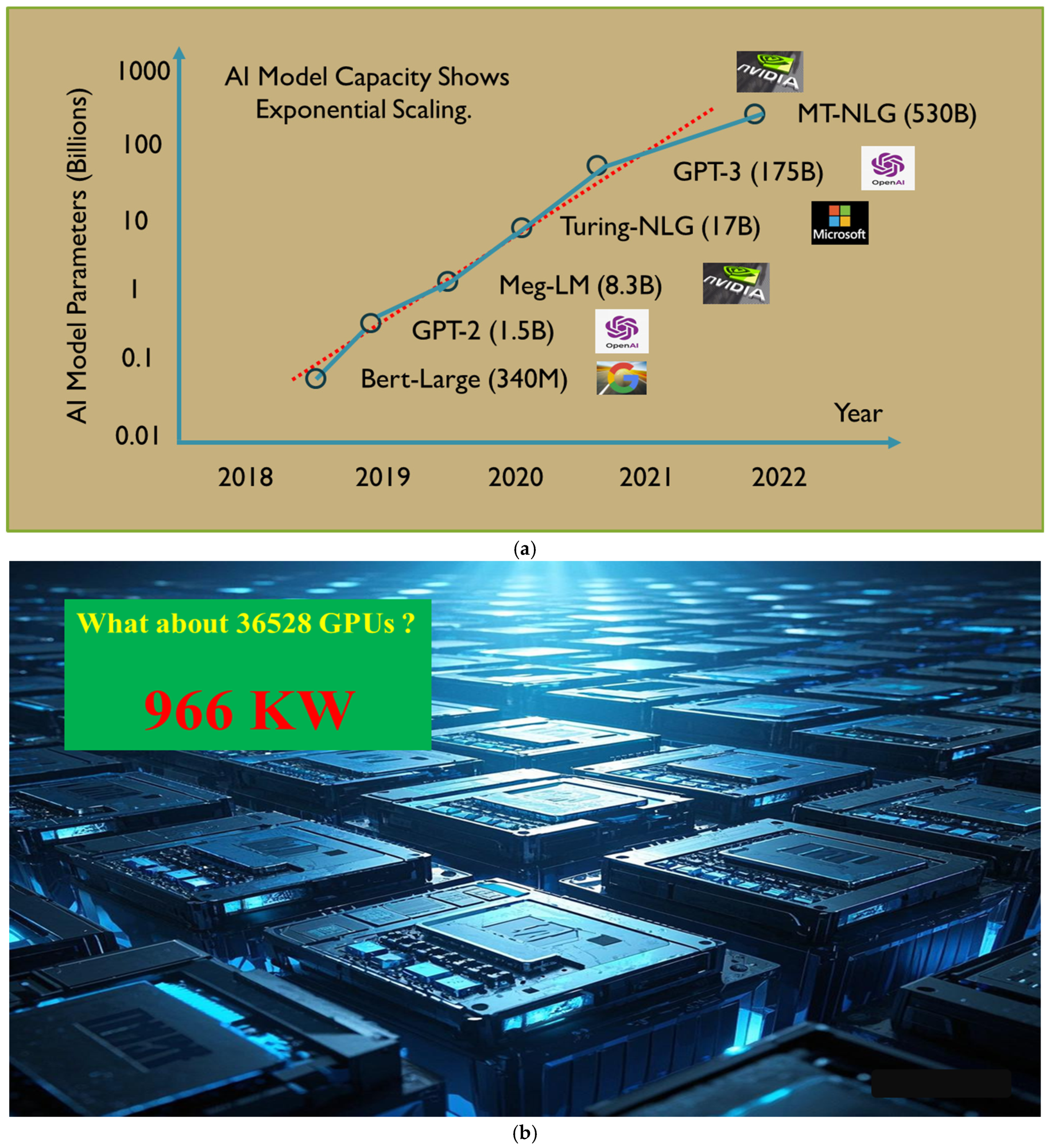
1. Introduction
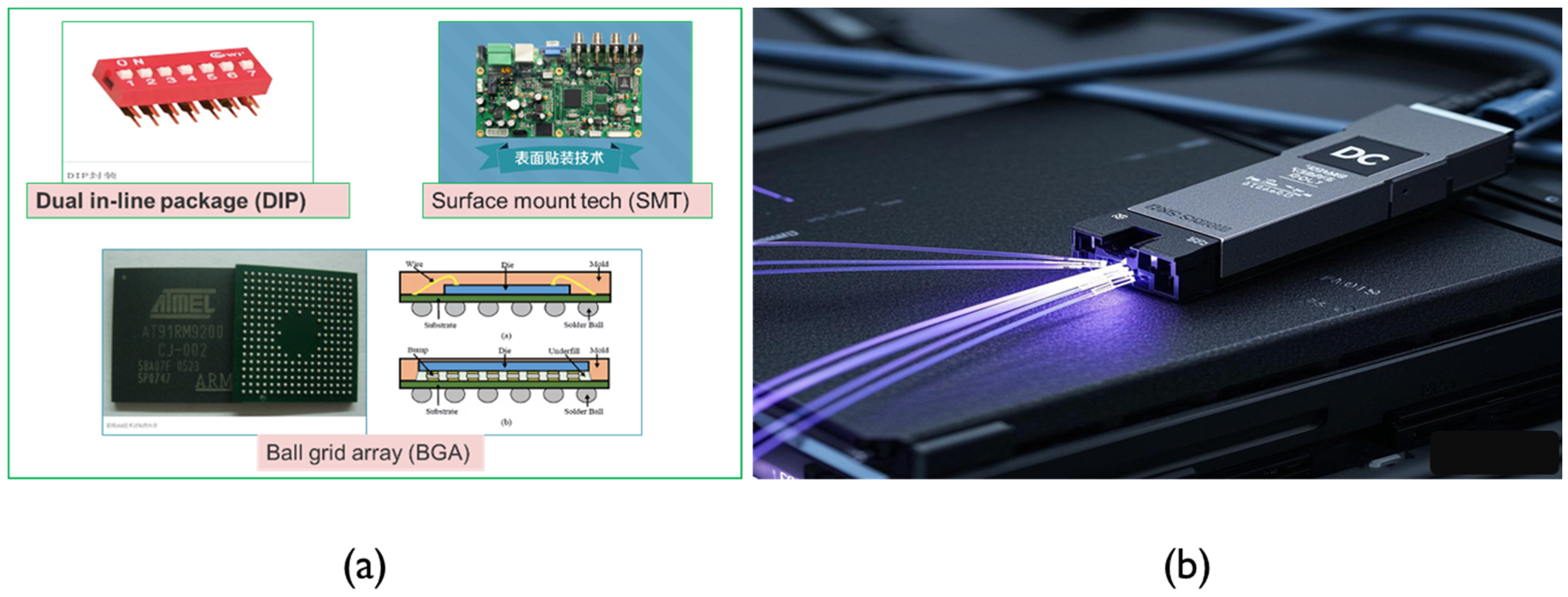
2. Conventional Packaging Technology
2.1. Dual In-Line Package (DIP)
2.2. Surface Mount Technology (SMT)
2.2.1. SOP (Small Outline Package)
2.2.2. QFN (Quad Flat No-Lead)
2.2.3. QFP (Quad Flat Package)
2.2.4. SOT (Small Outline Transistor)
2.3. Ball Grid Array (BGA)
2.4. Flip-Chip (FC)
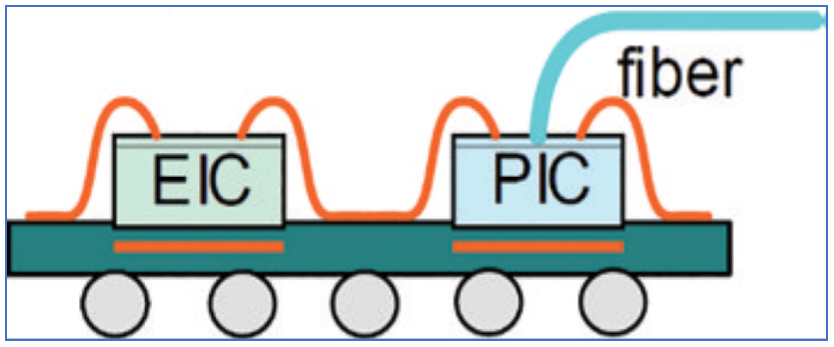
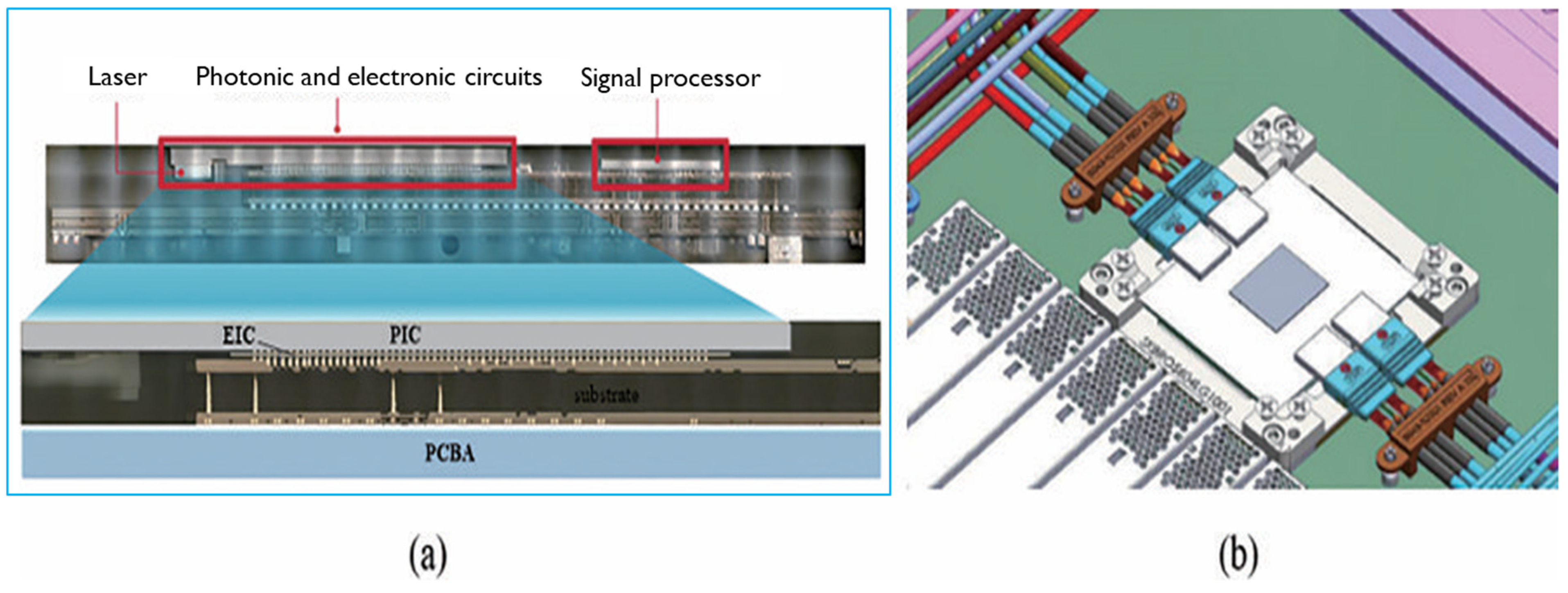
2.5. Optical Module
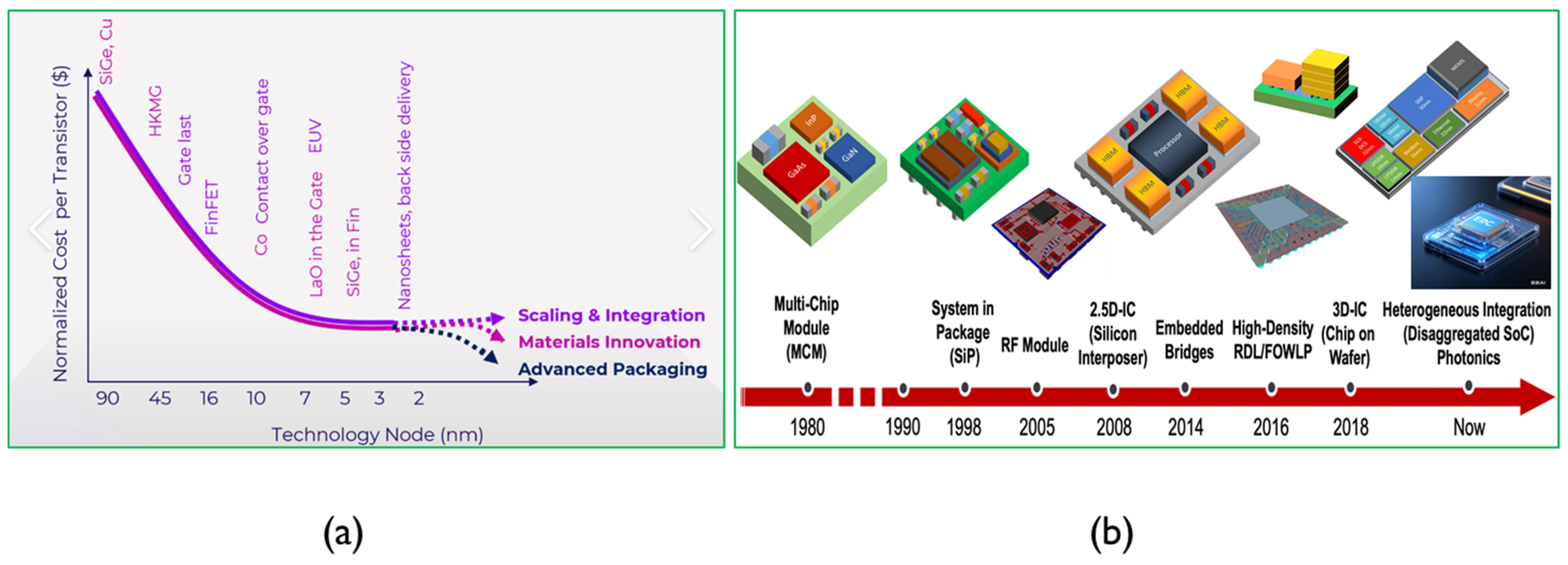
3. Advanced Packaging Technology
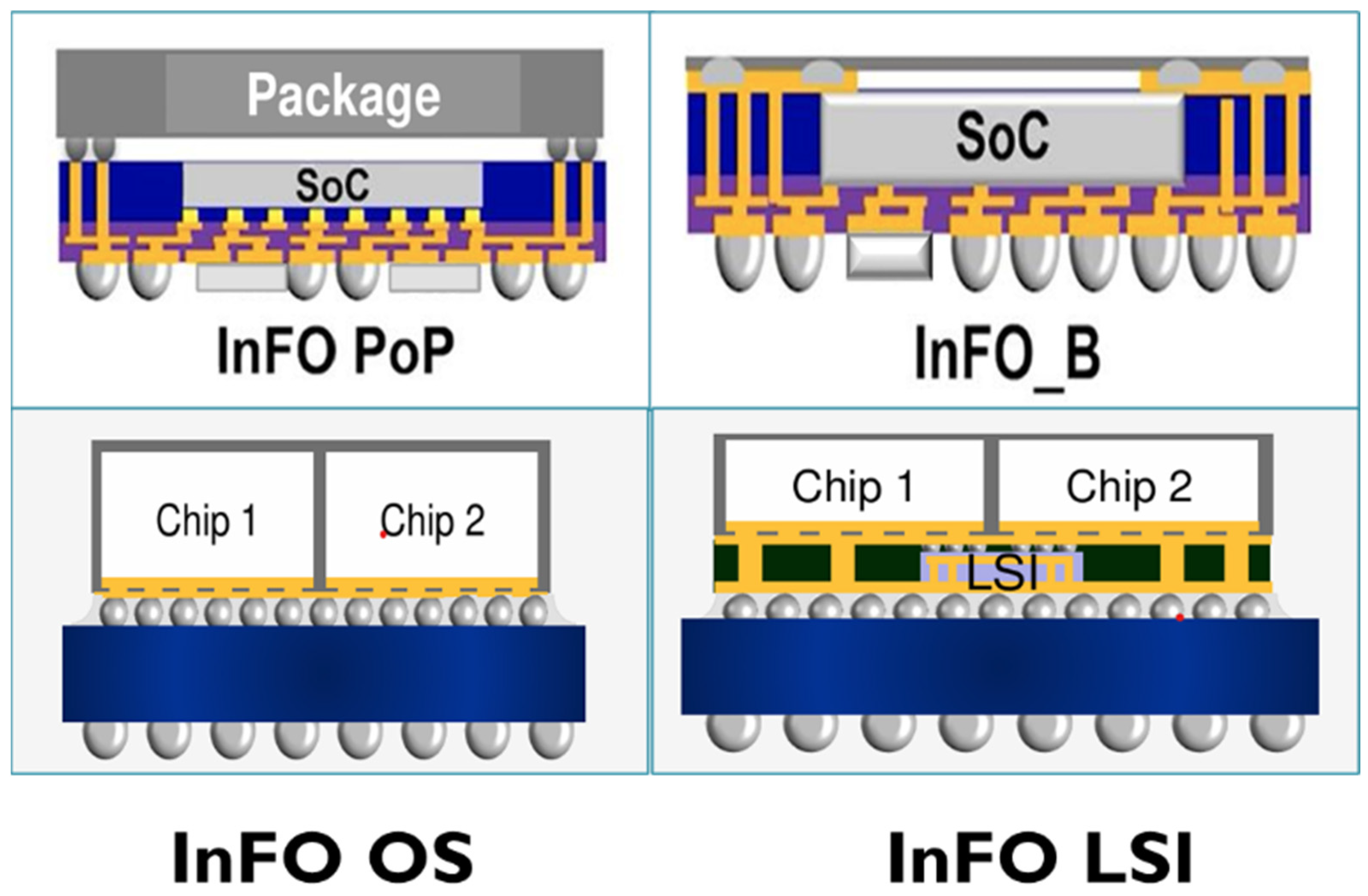
3.1. Fan-Out (FO) Package
3.2. Advanced 2D Packaging
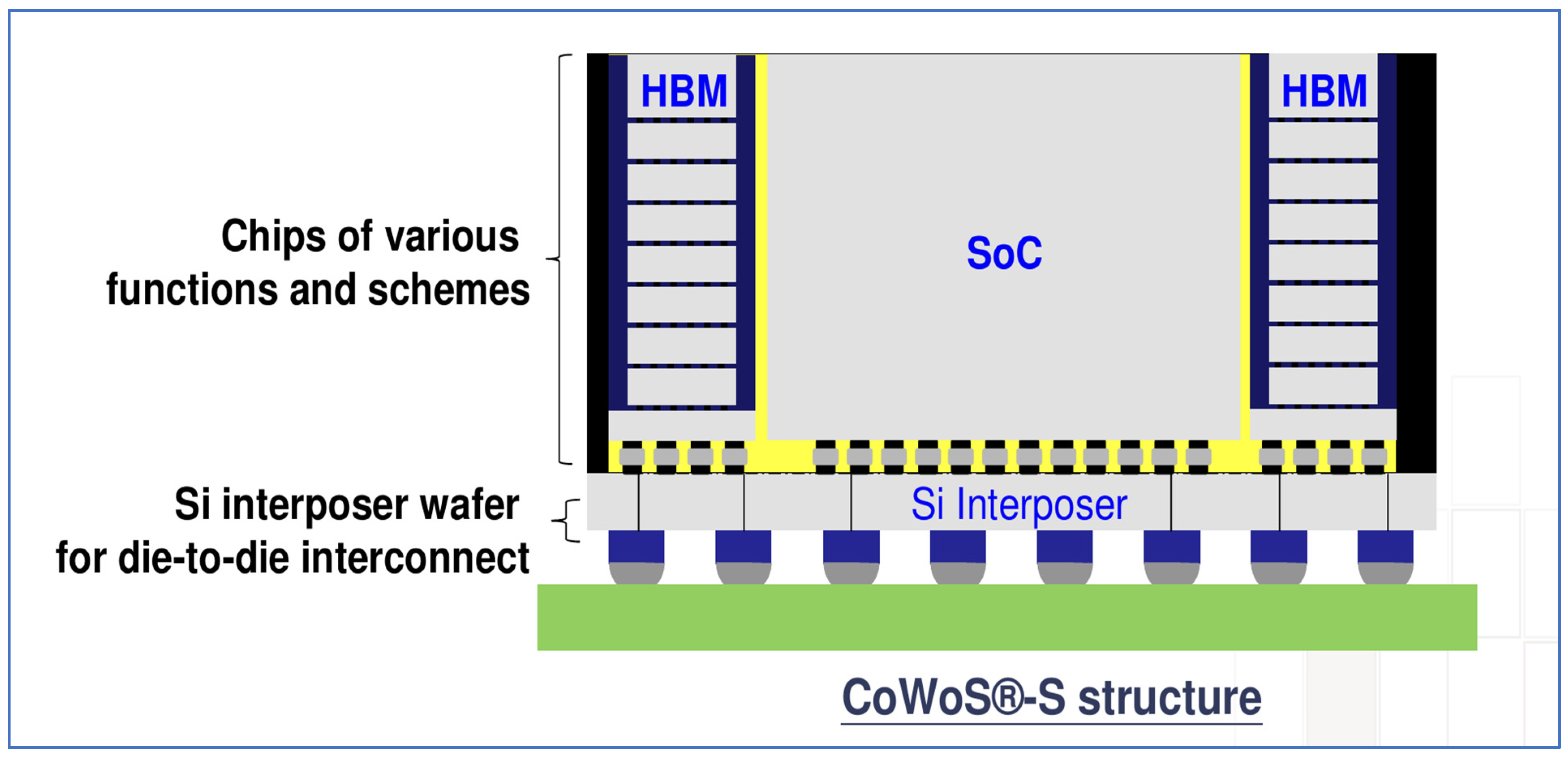
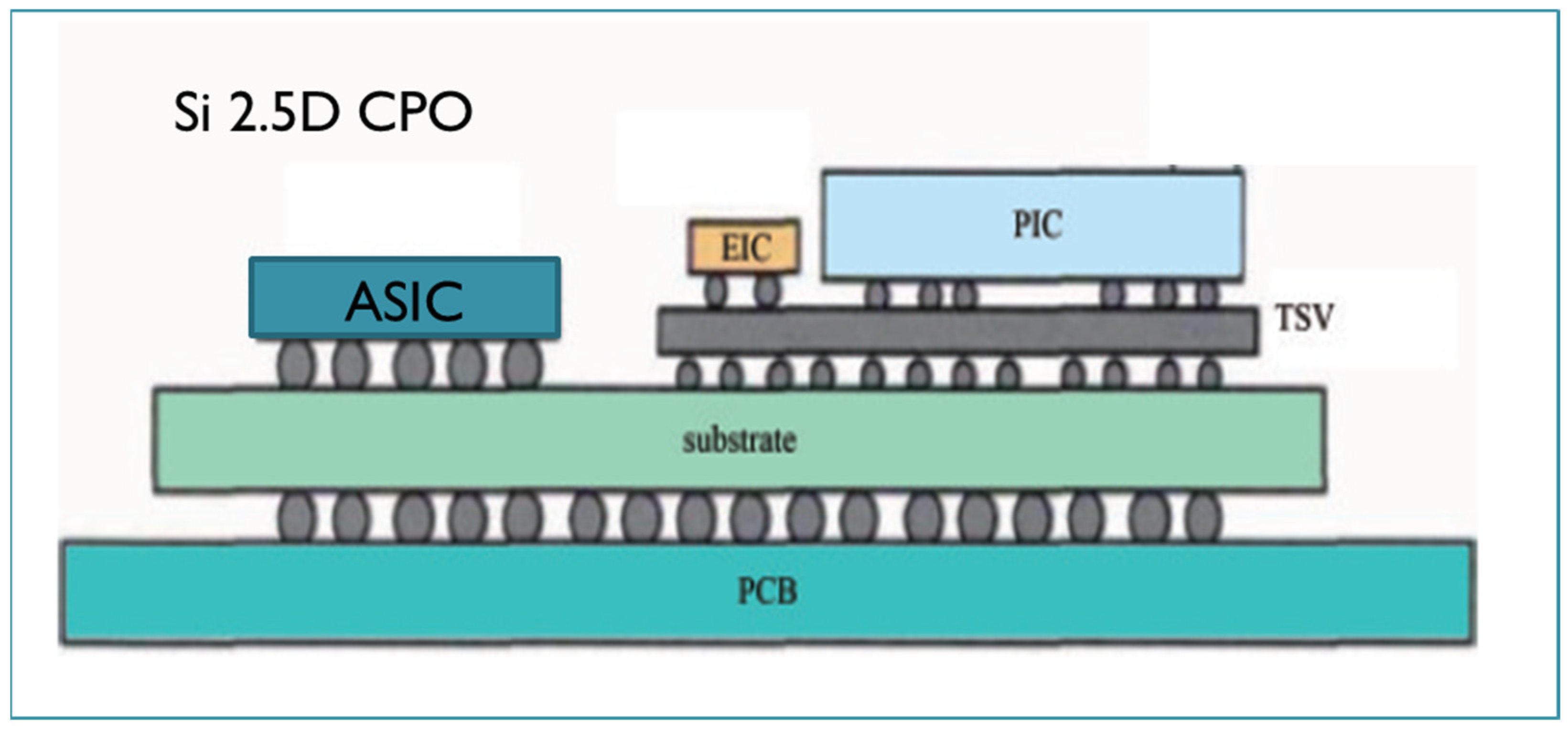
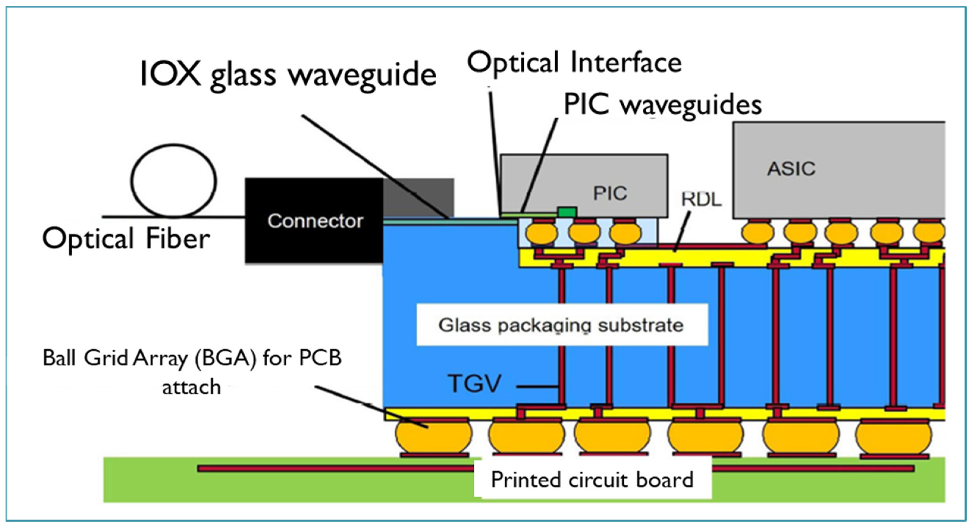
3.3. Silicon or Glass 2.5D Packaging
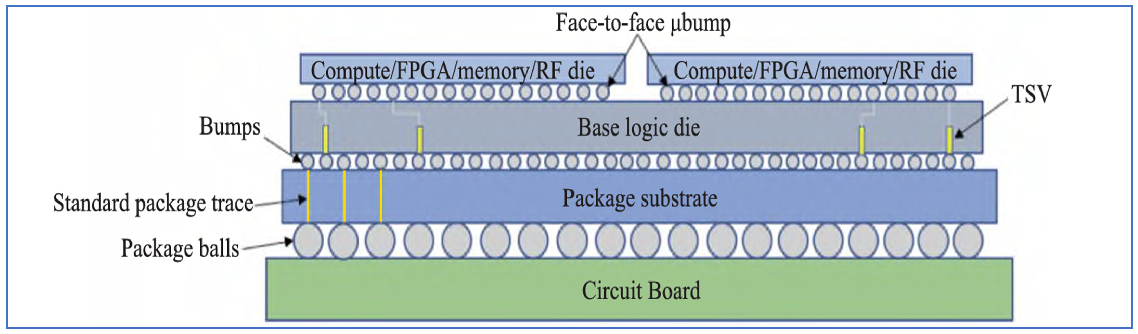
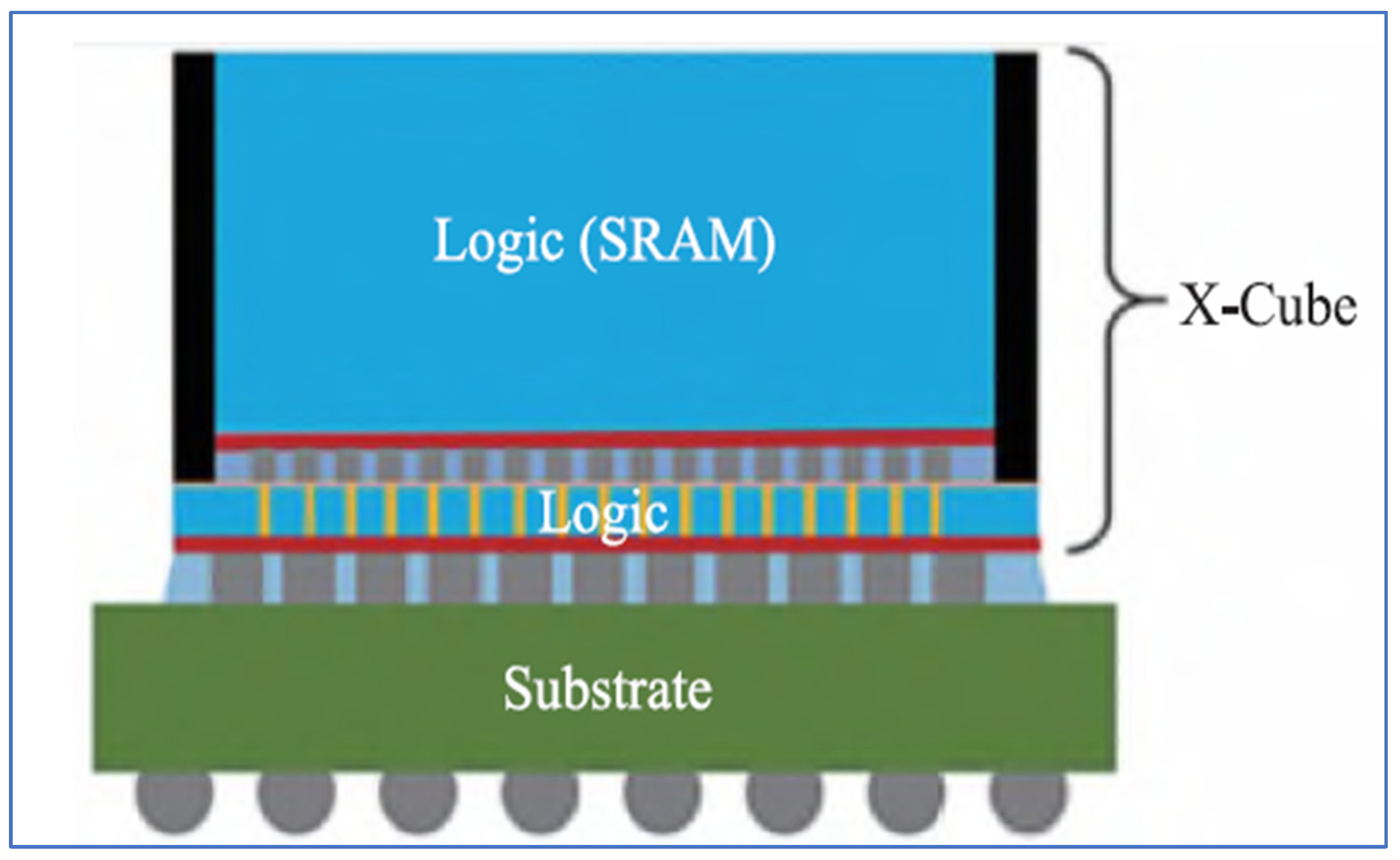
3.4. Silicon or Glass 3D Packaging
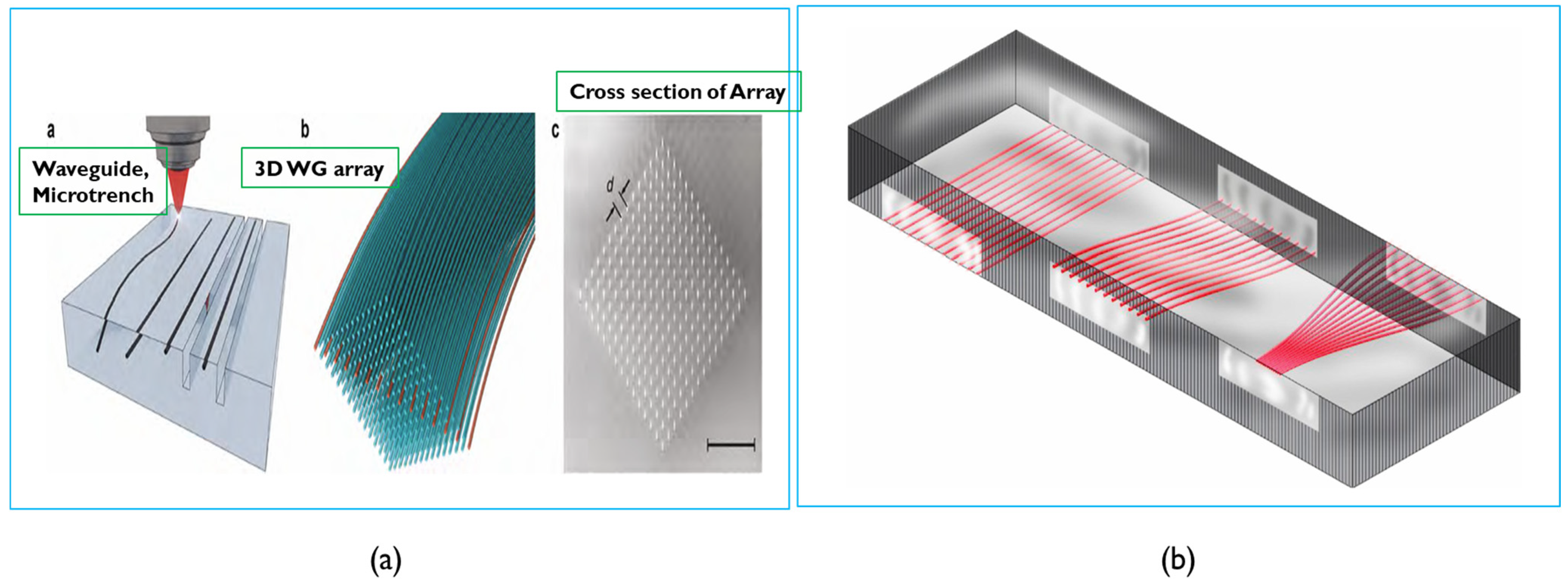
4. Future Prospects
5. Concluding Remark
Author Contributions
Funding
Conflicts of Interest
References
- Amodei, D.; Hernandez, D.; Sastry, G.; Clark, J.; Brockman, G.; Sutskever, I. AI and compute [EB/OL]. Available online: https://openai.com/index/ai-and-compute/ (accessed on 16 May 2018).
- Pancholy, R. Will You Need CPO in 3 Years? Broadcom ECOC: Frankfurt, Germany, 2024. [Google Scholar]
- Sun, Y.; Liu, F.M.; Xue, H.Y. High-speed and high-density optoelectronic co-package technologies. ZTE Technol. J. 2018, 24, 27–32. [Google Scholar]
- Margalit, N.; Xiang, C.; Bowers, S.M.; Bjorlin, A.; Blum, R.; Bowers, J.E. Perspective on the future of silicon photonics and electronics. Appl. Phys. Lett. 2021, 118, 220501. [Google Scholar] [CrossRef]
- Cheng, J.W.; Jiang, X.Y.; Zhou, H.L.; Wang, X.L.; Li, Y.; Zhang, W.; Liu, C. Research progress and challenges of photoelectric intelligent computing. Chin. J. Lasers 2022, 49, 1219001. [Google Scholar]
- Minkenberg, C.; Krishnaswamy, R.; Zilkie, A.; Nelson, D. Copackaged datacenter optics: Opportunities and challenges. IET Opto-Electron. 2021, 15, 77–91. [Google Scholar]
- Ou, X.P.; Yang, Z.L.; Tang, B.; Li, Z.H.; Luo, J.; Wang, W.W.; Yang, Y. 2.5D/3D silicon-based optoelectronic integration technology and its application. Study Opt. Commun. 2023, 49, 1–16. [Google Scholar]
- Johnson, J.E.; Bacher, K.; Schaevitz, R.; Raghunathan, V. Performance and Reliability of Advanced CW Lasers for Silicon Photonics Applications. In Proceedings of the 2022 Optical Fiber Communications Conference and Exhibition (OFC), San Diego, CA, USA, 6–10 March 2022; IEEE Press: Piscataway, NJ, USA, 2022. [Google Scholar]
- Cheng, Q.X.; Bahadori, M.; Glick, M.; Rumley, S.; Bergman, K. Recent advances in optical technologies for data centers: A review. Optica 2018, 5, 1354–1370. [Google Scholar]
- Tan, M.; Xu, J.; Liu, S.Y.; Feng, J.; Zhang, H.; Yao, C.; Chen, S.; Guo, H.; Han, G.; Wen, Z.; et al. Co-packaged optics (CPO): Status, challenges, and solutions. Front. Optoelectron. 2023, 16, 1–40. [Google Scholar] [PubMed]
- Mahajan, R.; Li, X.Q.; Fryman, J.; Zhang, Z.; Nekkanty, S.; Tadayon, P.; Jaussi, J.; Shumarayev, S.; Agrawal, A.; Jadhav, S. Co-packaged photonics for high performance computing: Status, challenges and opportunities. J. Light. Technol. 2022, 40, 379–392. [Google Scholar] [CrossRef]
- Thomson, D.; Zilkie, A.; Bowers, J.E.; Komljenovic, T.; Reed, G.T.; Vivien, L.; Marris-Morini, D.; Cassan, E.; Virot, L.; Fédéli, J.-M. Roadmap on silicon photonics. J. Opt. 2016, 18, 073003. [Google Scholar]
- Butkutė, A.; Jonušauskas, L. 3D Manufacturing of Glass Microstructures Using Femtosecond Laser. Micromachines 2021, 12, 499. [Google Scholar] [CrossRef]
- Xie, Q.; Shchedrina, N.; Cavillon, M.; Poumellec, B.; Lancry, M. Nanoscale investigations of femtosecond laser induced nanogratings in optical glasses. Nanoscale Adv. 2024, 6, 489–498. [Google Scholar] [PubMed]
- Zaiter, R.; Lancry, M.; Fargues, A.; Adamietz, F.; Dussauze, M.; Rodriguez, V.; Poumellec, B.; Cardinal, T. Optical and structural characterization of femtosecond laser written microstructures in germanate glass. Sci. Rep. 2023, 13, 11050. [Google Scholar] [CrossRef] [PubMed]
- Wang, Y.D.; Li, Z.Z.; Li, Y.C.; Duan, Y.Z.; Wang, L.C.; Yu, Y.H.; Chen, Q.D. Ultralow birefringent glass waveguide fabricated by femtosecond laser direct writing. Opt. Lett. 2023, 48, 554–557. [Google Scholar] [PubMed]
- Martinell, J.M. A Modular Packaging Approach for Dual In-Line Integrated Circuits; SAE Technical Paper 670207; SAE: Warminster, PA, USA, 1967. [Google Scholar]
- Hardisty, H.; Abboud, J. Thermal analysis of a dual-in-line package using the finite-element method. IEE Proc. Solid State Electron Devices 1987, 134, 23–28. [Google Scholar] [CrossRef]
- Lowryuwen, C.J.; Kennimer, B.L.; Miller, L. A Reliable Dry Ceramic Dual In-Line Package (CERDIP). In Proceedings of the IEEE International Reliability Physics Symposium, San Diego, CA, USA, 18–20 April 1978. [Google Scholar]
- Technical Staff, ICE Corporation. Surface Mount Packaging Report; Semiconductor International: New York, NY, USA, 1986; pp. 72–77. [Google Scholar]
- Prasad, P. Contributing factors for thermal damage in PWB assemblies during hand soldering. IPC Tech. Rev. 1982, 9–17. [Google Scholar]
- Nakahara, H. Japan’s swing to chip-on-board. Electron. Packag. Prod. 1986, 38–41. [Google Scholar]
- Alli, M.; Mahalingam, M.; Andrews, J. Thermal Characteristics of Plastic Small Outline Transistor (SOT) Packages. IEEE Trans. Compon. Hybrids Manuf. Technol. 1986, 9, 353–363. [Google Scholar] [CrossRef]
- Shi, Y.; Chen, H.; Wu, J.; Shiu, I.; Wong, F. Thermo-Mechanical Analysis and Design for SOD Package Based on Finite Element Method. IEEE Trans. Compon. Packag. Manuf. Technol. 2012, 2, 650–659. [Google Scholar]
- Lu, A.C.W.; Xie, D.J.; Shi, Z.F.; Ryu, W. Electrical and thermal modelling of QFN packages. In Proceedings of the 3rd Electronics Packaging Technology Conference (EPTC 2000) (Cat. No. 00EX456), Singapore, 7 December 2000; pp. 352–356. [Google Scholar]
- Fu, J.; Huang, H.; Zhang, C. Thermal Resistance Modeling to Analyze and Simulate of Quad Flat No-Leads Packaging on Printed Circuit Board by Using ANSYS. In Proceedings of the 2024 IEEE 7th International Electrical and Energy Conference (CIEEC), Harbin, China, 12 May 2024; pp. 3950–3955. [Google Scholar]
- Guenin, B.M.; Mahulikar, D.; Leslie, D.C.; Holmes, M. Reliability and performance of non-hermetic, surface-mount quad flat packages. In Proceedings of the 1994 44th Electronic Components and Technology Conference, Washington, DC, USA, 1–4 May 1994; pp. 721–727. [Google Scholar]
- Lee, C.C.; Chien, D.H. A thermally enhanced plastic package with indented leadframe. In Proceedings of the 1997 Proceedings 47th Electronic Components and Technology Conference, San Jose, CA, USA, 18–21 May 1997; pp. 338–342. [Google Scholar]
- Han, J.; Chen, H.; Xue, K.; Wong, F.; Leung, K.; Shiu, I.; Wu, J. Wire sweep study for SOT package array matrix molding with simulation and experimental analysis. In Proceedings of the 2011 12th International Conference on Electronic Packaging Technology and High Density Packaging, Shanghai, China, 8–11 August 2011; pp. 1–6. [Google Scholar]
- Huang, J.; Huang, X.; Shi, K.; Cheng, X.; Jiang, Y. Mold Flow Analysis and Optimization in Injection Molding Process for Semiconductor Packages. In Proceedings of the 2022 23rd International Conference on Electronic Packaging Technology (ICEPT), Dalian, China, 10–13 August 2022; pp. 1–5. [Google Scholar]
- Liu, J.J.; Berg, H.; Wen, Y.; Mulgaonker, S.; Bowlby, R.; Mawer, A. Plastic ball grid array (PBGA) overview. Mater. Chem. Phys. 1995, 40, 236–244. [Google Scholar]
- Liu, X.; Xu, S.; Lu, G.Q.; Dillard, D.A. Stacked solder bumping technology for improved solder joint reliability. Microelectron. Reliab. 2001, 41, 1979–1992. [Google Scholar]
- Ong, E.E.S.; Abdullah, M.Z.; Khor, C.Y.; Loh, W.K.; Ooi, C.K.; Chan, R. Analysis of encapsulation process in 3D stacked chips with different microbump array. Int. Commun. Heat Mass Transf. 2012, 39, 1616–1623. [Google Scholar]
- Xiao, Y.; Shah, H.N.; Natarajan, R.; Rymaszewski, E.J.; Chow, T.P.; Gutmann, R.J. Integrated flip-chip flex-circuit packaging for power electronics applications. IEEE Trans. Power Electron. 2004, 19, 515–522. [Google Scholar] [CrossRef]
- Mohan, R.; Sharma, P. Reliability analysis of flip-chip packaging: Effects of bump size and interfacial stresses. Microelectron. Reliab. 2013, 53, 1623–1630. [Google Scholar]
- Park, K.; Kim, Y. Flip-chip package technology: A comprehensive review of bumping and assembly techniques. J. Electron. Mater. 2011, 40, 1481–1490. [Google Scholar]
- Botez, D.; Herskowitz, G.J. Components for optical communications systems: A review. Proc. IEEE 1980, 68, 689–731. [Google Scholar] [CrossRef]
- Vaughan, D.; Hannah, R.; Fields, M. Applications for Embedded Optic Modules in Data Communications; Avago Technologies White Paper; Avago Technologies: Singapore, 2011. [Google Scholar]
- Zhang, F.; Xiong, L.; Min, R.; Guo, Y.; Wang, Z.; Xiao, K. A Miniaturized Optical Communication Module: Design, Development, and Testing. In Proceedings of the 2024 IEEE 12th International Conference on Information, Communication and Networks (ICICN), Guilin, China, 21–24 August 2024; pp. 132–139. [Google Scholar] [CrossRef]
- Douglas, Y. TSMC Packaging Technologies for Chiplets and 3D. In Proceedings of the 2021 IEEE Hot Chips, Palo Alto, CA, USA, 22–24 August 2021; Volume 33, pp. 47–56. [Google Scholar]
- Tseng, C.F.; Liu, C.S.; Wu, C.H.; Yu, D. InFO (Wafer Level Integrated Fan-Out) Technology. In Proceedings of the 2016 IEEE 66th Electronic Components and Technology Conference (ECTC), Las Vegas, NV, USA, 31 May–3 June 2016; pp. 1–6. [Google Scholar] [CrossRef]
- Mii, Y.J. Semiconductor Innovations, from Device to System. In Proceedings of the 2022 IEEE Symposium on VLSI Technology and Circuits (VLSI Technology and Circuits), Honolulu, HI, USA, 13–17 June 2022; pp. 276–281. [Google Scholar] [CrossRef]
- Wang, C.-T.; Yu, D. Signal and Power Integrity Analysis on Integrated Fan-Out PoP (InFO_PoP) Technology for Next Generation Mobile Applications. In Proceedings of the 2016 IEEE 66th Electronic Components and Technology Conference (ECTC), Las Vegas, NV, USA, 31 May–3 June 2016; pp. 380–385. [Google Scholar]
- Zhang, C.; Chang, J.; Lu, X. Packaging Technologies for 3D Integration: InFO PoP and Beyond. J. Microelectron. Electron. Packag. 2017, 14, 45–53. [Google Scholar]
- Chen, J.; Chen, L.; Zhang, X. Development and Applications of InFO Bump Technology for Advanced Packaging Solutions. In Proceedings of the 67th Electronic Components and Technology Conference (ECTC), Lake Buena Vista, FL, USA, 30 May–2 June 2017; pp. 934–939. [Google Scholar]
- Liu, H.; Li, W.; Zhang, Y. Enhanced Performance and Reliability of InFO Bump Packaging for High-Density Devices. J. Electron. Mater. 2018, 47, 1322–1329. [Google Scholar]
- Wang, L.; Cheng, T. Fan-Out Wafer-Level Packaging with Open Substrate Integration for Advanced ICs. IEEE Trans. Compon. Packag. Manuf. Technol. 2020, 10, 1241–1248. [Google Scholar]
- Huang, Z.; Lee, Y. InFO OS Technology: Enabling High-Density, High-Performance Semiconductor Packaging Solutions. IEEE J. Microelectron. Packag. 2021, 15, 453–459. [Google Scholar]
- Chen, T.; Tsai, H. InFO LSI: A Novel Integration of Logic and Memory Functions for Advanced Packaging Solutions. IEEE Trans. Adv. Packag. 2022, 12, 145–152. [Google Scholar]
- Zhang, X.; Lin, W. The Evolution of InFO LSI Technology for System Integration in Semiconductor Packaging. IEEE J. Microelectron. Packag. 2021, 8, 115–121. [Google Scholar]
- Wang, S.; Liu, M. InFO MS: A Next-Generation 3D Packaging Solution for High-Performance Applications. IEEE Trans. Compon. Packag. Manuf. Technol. 2021, 11, 1332–1338. [Google Scholar]
- Huang, J.; Zhang, Y. InFO MS Technology: Enabling Compact and High-Performance Multi-Stack Packaging for Advanced Electronics. IEEE J. Microelectron. Packag. 2022, 16, 400–407. [Google Scholar]
- Zhang, Y.P.; Liu, D. Antenna-on-Chip and Antenna-in-Package Solutions to Highly Integrated Millimeter-Wave Devices for Wireless Communications. IEEE Trans. Antennas Propag. 2009, 57, 2830–2841. [Google Scholar] [CrossRef]
- Wang, X.; Chen, L. The Development and Applications of InFO-AiP for 5G and Beyond. IEEE J. Solid-State Circuits 2021, 56, 1812–1820. [Google Scholar]
- Lau, J.H. Recent Advances and Trends in Advanced Packaging. IEEE Trans. Compon. Packag. Manuf. Technol. 2022, 12, 228–252. [Google Scholar] [CrossRef]
- Wang, J.; Xu, L. The Evolution of 2D Packaging Technologies in Semiconductor Industry: Challenges and Solutions. IEEE J. Microelectron. Packag. 2021, 17, 234–242. [Google Scholar]
- Zhang, W.; Liu, Y. Design and Fabrication of Advanced 2D Semiconductor Packages for High-Performance ICs. IEEE Trans. Adv. Packag. 2022, 14, 525–532. [Google Scholar]
- Jiang, H.; Chen, J. Exploring 2D Semiconductor Package Integration for High-Speed Applications. IEEE J. Solid-State Circuits 2021, 58, 1954–1961. [Google Scholar]
- Lee, K.; Park, D. Next-Generation 2D Packaging Solutions for Efficient and Compact Integrated Circuits. IEEE Trans. Compon. Packag. Manuf. Technol. 2020, 9, 1020–1027. [Google Scholar]
- Sun, S.; Wang, Q. Advanced 2D Semiconductor Packaging: A Path to Enhanced Performance and Miniaturization. IEEE Trans. Electron Devices 2021, 68, 4773–4780. [Google Scholar]
- Bian, L.Y.; Zeng, Y.P.; Cai, Y.; Lu, X.; Zhou, Q.R.; Tang, Q.L.; Gu, T.W.; Wang, L. Opportunities and Challenges of Co-packaged optics Technology in the Era of Big Data. Prog. Laser Optoelectron. 2024, 61, 1211. [Google Scholar]
- Tan, M.; Rosenberg, P.; Sorin, W.; Mathai, S.; Panotopoulos, G.; Rankin, G. Universal photonic interconnect for data centers. In Proceedings of the 2017 Optical Fiber Communications Conference and Exhibition (OFC), Los Angeles, CA, USA, 21–23 March 2017; pp. 1–3. [Google Scholar]
- Hsia, H.; Tsai, C.H.; Ting, K.C.; Kuo, F.W.; Lin, C.C.; Wang, C.T.; Hou, S.Y.; Chiou, W.C.; Douglas, C.H.Y. Heterogeneous Integration of a Compact Universal Photonic Engine for Silicon Photonics Applications in HPC. In Proceedings of the 2021 IEEE 71st Electronic Components and Technology Conference (ECTC), San Diego, CA, USA, 1–4 July 2021; pp. 263–268. [Google Scholar]
- Liu, Z.; Yu, D. The COUPE Design for Next-Generation Optical Interconnects in AI and Networking Systems. IEEE J. Light. Technol. 2021, 39, 1023–1030. [Google Scholar]
- Yoon, S.W.; Na, D.J.; Choi, W.K.; Kang, K.T.; Yong, C.B.; Kim, Y.C.; Marimuthu, P.C. 2.5D/3D TSV processes development and assembly/packaging technology. In Proceedings of the 2011 IEEE 13th Electronics Packaging Technology Conference, Singapore, 7–9 December 2011; pp. 336–340. [Google Scholar]
- Chan, F.; Chan, H.; Choy, K. A systematic approach to manufacturing packaging logistics. Int. J. Adv. Manuf. Technol. 2006, 29, 1088–1101. [Google Scholar] [CrossRef]
- Lee, C.H.; Kim, S. Advancements in 2.5D and 3D packaging for high-performance computing and communication systems. IEEE Trans. Adv. Packag. 2020, 43, 250–259. [Google Scholar]
- Lin, L.; Yeh, T.C.; Wu, J.L.; Lu, G.; Tsai, T.F.; Chen, L.; Xu, A.T. Reliability characterization of Chip-on-Wafer-on-Substrate (CoWoS) 3D IC integration technology. In Proceedings of the 2013 IEEE 63rd Electronic Components and Technology Conference, Las Vegas, NV, USA, 28–31 May 2013; pp. 366–371. [Google Scholar]
- Mii, Y.J. Semiconductor Industry Outlook and New Technology Frontiers. In Proceedings of the 2024 IEEE International Electron Devices Meeting (IEDM), San Francisco, CA, USA, 7–11 December 2024; pp. 1–6. [Google Scholar] [CrossRef]
- Wang, H.H.; Liu, S. Chip-on-Wafer-on-Substrate (CoWoS) technology: Integration of multiple dies for high-performance applications. Microelectron. J. 2018, 72, 35–42. [Google Scholar]
- Tian, W.C.; Xie, H.L.; Chen, Y.M.; Zhao, J.R.; Zhang, G.G. Advanced package technology for AI chips. Electron. Packag. 2024, 24, 1–6. [Google Scholar]
- Li, L.; Chia, P.; Ton, P.; Nagar, M.; Patil, S.; Xue, J.; Delacruz, J.; Voicu, M.; Hellings, J.; Isaacson, B.; et al. 3D SiP with Organic Interposer for ASIC and Memory Integrationl. In Proceedings of the 2016 IEEE 66th Electronic Components and Technology Conference (ECTC), Las Vegas, NV, USA, 31 May–3 June 2016; pp. 1445–1450. [Google Scholar]
- Lau, J.H. Multiple System and Heterogeneous Integration with TSV-Interposers. In Chiplet Design and Heterogeneous Integration Packaging; Springer: Singapore, 2023. [Google Scholar]
- Jung, K.; Lee, J. A Comprehensive Review of 2.5D Interposer Technology: Samsung I-Cube4 and Its Applications. IEEE Trans. Adv. Packag. 2020, 14, 279–286. [Google Scholar]
- Ge, C.; Wang, X.Y.; Du, J.B.; Lin, X.Z.; Lei, T.; Du, L.P.; He, Z.Y. High-speed wafer-level TGV interposer for 2.5D CPO. Opt. Commun. 2025, 579, 131517. [Google Scholar] [CrossRef]
- Brusberg, L.; Grenier, J.R.; Zakharian, A.R.; Yeary, L.W.; Seok, S.H.; Noh, J.H.; Kim, Y.G.; Matthies, J.; Terwilliger, C.C.; Paddock, B.J.; et al. Glass Platform for Co-Packaged Optics. IEEE J. Sel. Top. Quantum Electron. 2023, 29, 1–10. [Google Scholar] [CrossRef]
- Kumar, A.; Verma, G.; Nath, V.; Choudhury, S. IC Packaging: 3D IC Technology and Methods. In Proceedings of the International Conference on Nano-Electronics, Circuits & Communication Systems, Chennai, India, 17–18 February 2017; Lecture Notes in Electrical Engineering. Nath, V., Ed.; Springer: Singapore, 2017; Volume 403. [Google Scholar]
- Zhang, D.; Lu, J.J.Q. 3D Integration Technologies: An Overview. In Materials for Advanced Packaging; Lu, D., Wong, C., Eds.; Springer: Cham, Switzerland, 2017. [Google Scholar]
- Zhou, J.; Song, Y. Microbump and TSV Integration for High-Density 3D Packaging Solutions. IEEE J. Solid-State Circuits 2018, 53, 3837–3844. [Google Scholar]
- Wang, Z.; Chen, Q. Exploring Through-Silicon Vias and Microbumps for Advanced 3D Integrated Packaging. IEEE Trans. Adv. Packag. 2017, 40, 219–227. [Google Scholar]
- Li, S.; Xie, Y. Fabrication and Characterization of TSVs and Microbumps in 3D Integrated Circuits. IEEE J. Microelectron. Packag. 2019, 25, 105–112. [Google Scholar]
- Kang, S.; Lee, H. The Impact of Through-Glass Vias (TGVs) and TSVs on the Performance of 3D Semiconductor Packages. IEEE Trans. Device Mater. Reliab. 2018, 18, 56–63. [Google Scholar]
- Min, M.; Kadivar, S. Accelerating Innovations in the New Era of HPC, 5G and Networking with Advanced 3D Packaging Technologies. In Proceedings of the 2020 International Wafer Level Packaging Conference (IWLPC), San Jose, CA, USA, 13–15 October 2020; pp. 1–6. [Google Scholar]
- Shin, J.; Eslampour, H.; Jeong, S.; Kim, W.; Yong, S.; Ahn, S.O.; Park, E.; Song, S. Signal Integrity of Die-to-Die Interface with Advanced Packages for Co-Packaged Optics. In Proceedings of the 2024 IEEE 33rd Conference on Electrical Performance of Electronic Packaging and Systems (EPEPS), Toronto, ON, Canada, 6–9 October 2024; pp. 1–3. [Google Scholar]
- Park, S.; Kim, M. High-Performance 3D Integration and Packaging Technologies for Semiconductor Applications. IEEE Trans. Electron Devices 2020, 67, 4072–4079. [Google Scholar]
- Lau, J.H. Flip Chip, Hybrid Bonding, Fan-In, and Fan-Out Technology; Springer: Berlin/Heidelberg, Germany, 2024. [Google Scholar]
- Trebino, R.; Lee, K.F. Femtosecond Laser Pulses: Principles and Applications. IEEE J. Quantum Electron. 1998, 34, 382–390. [Google Scholar]
- Maruo, S.; Kumagai, Y. Femtosecond Laser Micromachining: Principles and Applications. IEEE J. Sel. Top. Quantum Electron. 2006, 12, 1081–1088. [Google Scholar]
- Melloni, A.; Martin, M. Photonic Integrated Circuits: Technologies and Applications. IEEE J. Sel. Top. Quantum Electron. 2015, 21, 1154–1163. [Google Scholar]
- Xie, L.; Liu, Y. Recent Advances in Photonic Integrated Circuits for Communication and Sensing Applications. IEEE J. Light. Technol. 2017, 35, 1568–1575. [Google Scholar]
- Zhang, Q.; Dong, C. Quantum Integrated Circuits: Challenges and Advances in Quantum Computing Technologies. IEEE J. Sel. Top. Quantum Electron. 2018, 24, 880–888. [Google Scholar]
- Silverstone, J.M.; O’Brien, L. Quantum Integrated Circuits for Photonic Quantum Technologies. IEEE J. Light. Technol. 2018, 36, 2264–2272. [Google Scholar]
- Ming, D.; Wang, Y.; Wang, Z.; Wang, K.X.; Qiu, C.; Tan, M. EPHIC Models: General SPICE Photonic Models for Closed-Loop Electronic-Photonic Co-Simulation. IEEE Trans. Circuits Syst. I Regul. Pap. 2024, 71, 1819–1831. [Google Scholar] [CrossRef]
- Sen, L. Electronic-Photonic Co-Design of Silicon Photonic Interconnects. Ph.D. Thesis, University of California, Berkeley, CA, USA, 2017. [Google Scholar]
- Psaila, N.; Nekkanty, S.; Shia, D.; Tadayon, P. Detachable Optical Chiplet Connector for Co-Packaged Photonics. J. Light. Technol. 2023, 41, 6315–6323. [Google Scholar]
- Wang, Y.; Zhong, L.; Lau, K.Y.; Han, X.; Yang, Y.; Hu, J.; Firstov, S.; Chen, Z.; Ma, Z.; Tong, L.; et al. Precise Mode Control of Laser-Written Waveguides for Broadband, Low-Dispersion 3D Integrated Optics. Light Sci. Appl. 2024, 13, 130. [Google Scholar] [CrossRef] [PubMed]
- Grenier, J.R.; Brusberg, L.; Wieland, K.A.; Matthies, J.; Terwilliger, C.C. Ultrafast Laser Processing of Glass Waveguide Substrates for Multi-Fiber Connectivity in Co-Packaged Optics. Adv. Opt. Technol. 2023, 12, 1244009. [Google Scholar] [CrossRef]
- Iyer, S.; Samadi, G. Manufacturing Roadmap for Heterogeneous Integration and Electronics Packaging (MRHIEP); Final Report; UCLA CHIPS: Los Angeles, CA, USA, 2024. [Google Scholar]


| Parameter | DIP | SMT | BGA | Flip-Chip | Optical Module |
|---|---|---|---|---|---|
| I/O Density | Low (~64 pins) | Moderate | High (1000+ pins) | Very High | Moderate (fiber) |
| Thermal Performance | Poor | Moderate | Good | Requires underfill | Critical |
| Assembly Cost | Low | Low-Moderate | Moderate-High | High | Very High |
| Applications | Legacy systems | Consumer devices | HPC, GPUs | 5G, AI chips | Data centers |
| Reliability | Moderate | High | High | High (with underfill) | Moderate-High |
| Parameter | Fan-Out | Advanced 2D | 2.5D (Si/Glass) | 3D (Si/Glass) |
|---|---|---|---|---|
| I/O Density | 500–1000 I/O/mm2 | Up to 200 I/O/mm2 | 10 k–100 k I/O/cm2 | 10 k–1 M I/O/cm2 |
| Thermal Performance | Moderate | Good | High | Critical |
| Cost | $–$$ | $–$$ | $$$ | $$$$ |
| Key Applications | Mobile, RF | CPUs, ASICs | AI/GPU, HBM | HBM, Photonics |
| Complexity | Moderate | Low-Moderate | High | Very High |
| Desired Properties | Glass | Silicon | Organic Laminate | |
|---|---|---|---|---|
| TTV | <5 μm | Excellent | Good | Bad |
| Warp | <2 μm/20 mm | Excellent | Excellent | Bad |
| Insulation Resistance | High | Excellent | Bad | Good |
| Optical Transparency | Optical I/O | Excellent | Bad | Good |
| Surface Roughness | <5 nm | Excellent | Excellent | Bad |
| TCE | 3.2 ppm/C | Excellent | Excellent | Bad |
| Hermetic Vias | Mil-Spec | Excellent | Bad | Bad |
Disclaimer/Publisher’s Note: The statements, opinions and data contained in all publications are solely those of the individual author(s) and contributor(s) and not of MDPI and/or the editor(s). MDPI and/or the editor(s) disclaim responsibility for any injury to people or property resulting from any ideas, methods, instructions or products referred to in the content. |
© 2025 by the authors. Licensee MDPI, Basel, Switzerland. This article is an open access article distributed under the terms and conditions of the Creative Commons Attribution (CC BY) license (https://creativecommons.org/licenses/by/4.0/).
Share and Cite
Chen, G.; Wang, G.; Wang, Z.; Wang, L. Electronic Chip Package and Co-Packaged Optics (CPO) Technology for Modern AI Era: A Review. Micromachines 2025, 16, 431. https://doi.org/10.3390/mi16040431
Chen G, Wang G, Wang Z, Wang L. Electronic Chip Package and Co-Packaged Optics (CPO) Technology for Modern AI Era: A Review. Micromachines. 2025; 16(4):431. https://doi.org/10.3390/mi16040431
Chicago/Turabian StyleChen, Guoliang, Guiqi Wang, Zhenzhen Wang, and Lijun Wang. 2025. "Electronic Chip Package and Co-Packaged Optics (CPO) Technology for Modern AI Era: A Review" Micromachines 16, no. 4: 431. https://doi.org/10.3390/mi16040431
APA StyleChen, G., Wang, G., Wang, Z., & Wang, L. (2025). Electronic Chip Package and Co-Packaged Optics (CPO) Technology for Modern AI Era: A Review. Micromachines, 16(4), 431. https://doi.org/10.3390/mi16040431