

Wafer Bonding of GaAs and SiC via Thin Au Film at Room Temperature

Abstract
:1. Introduction
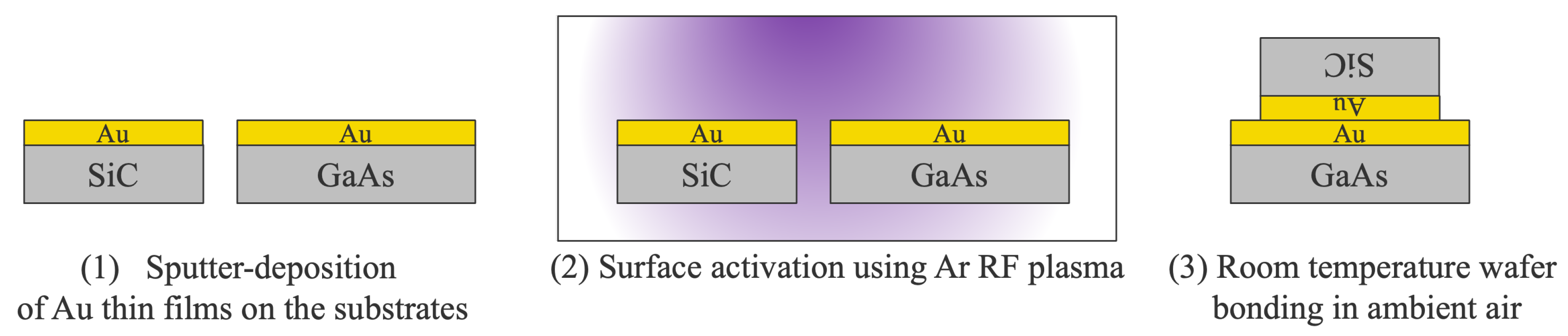
2. Methods
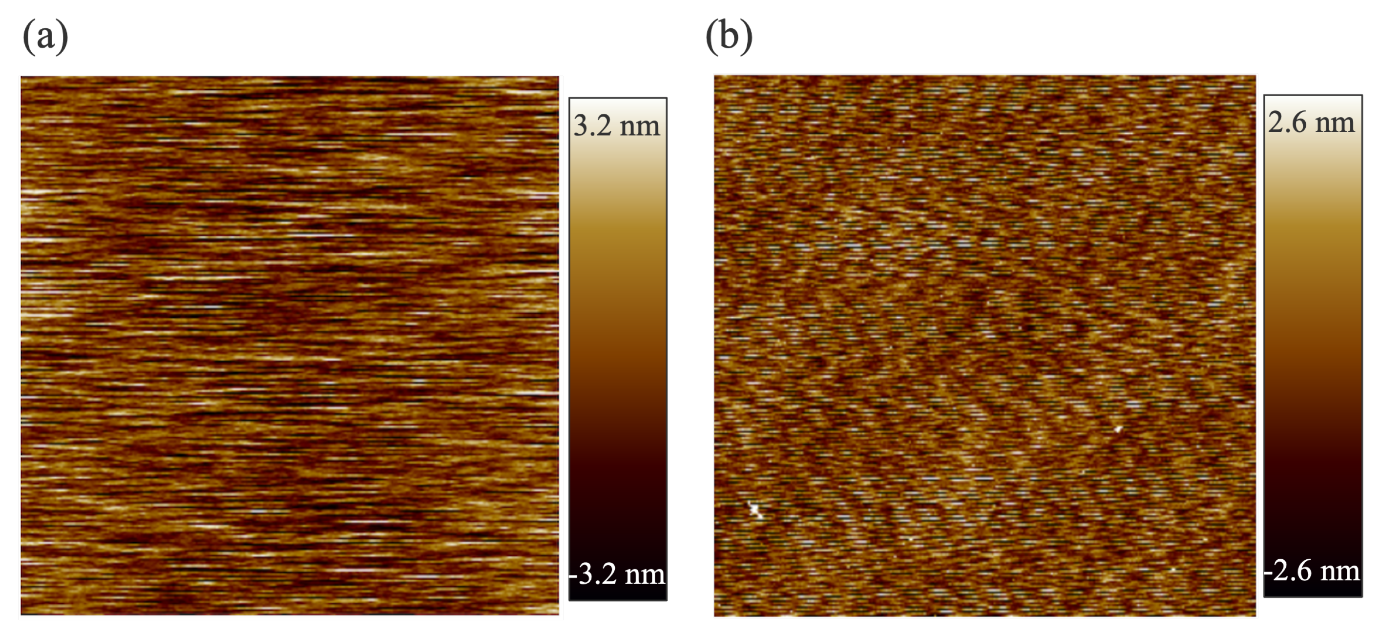
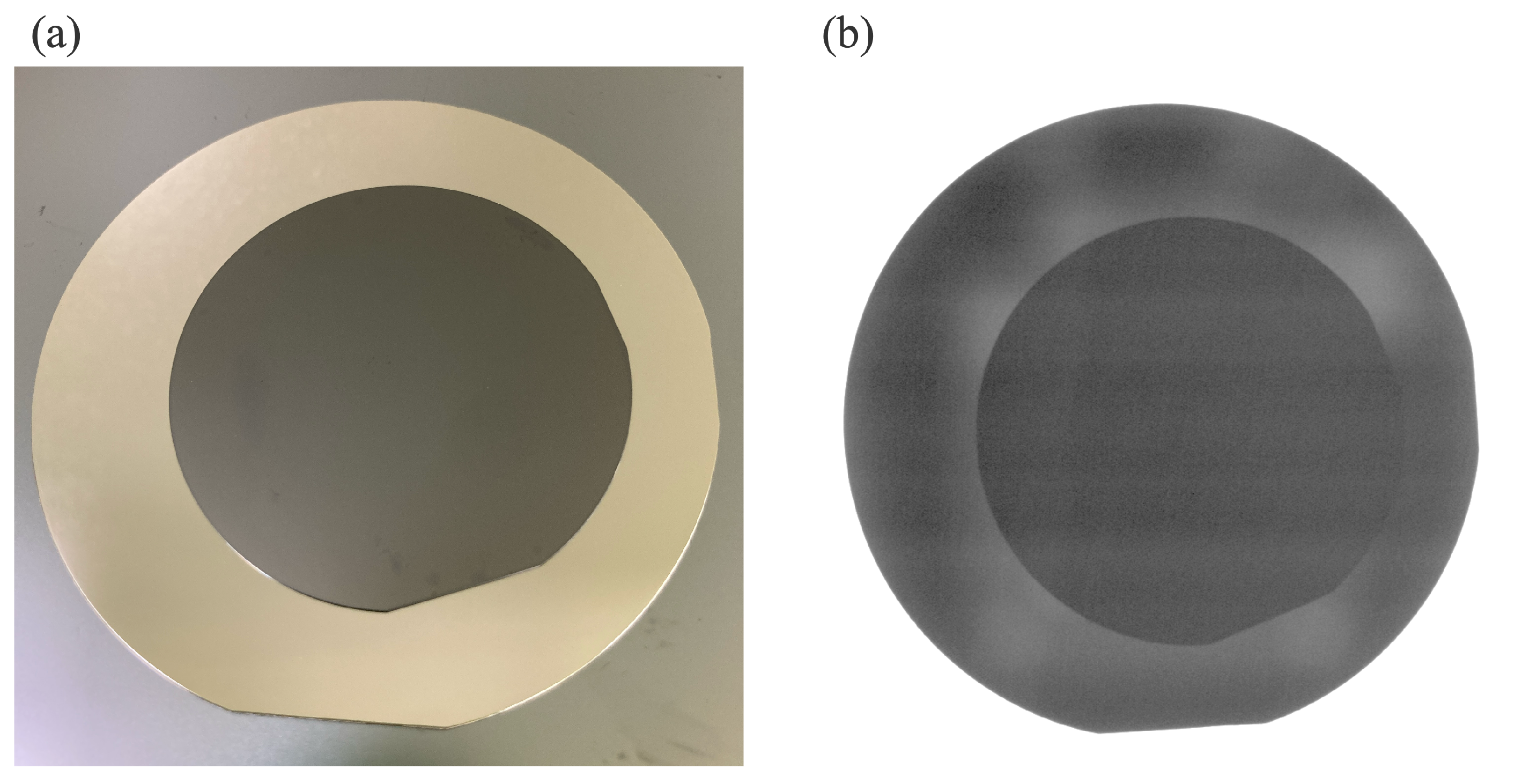
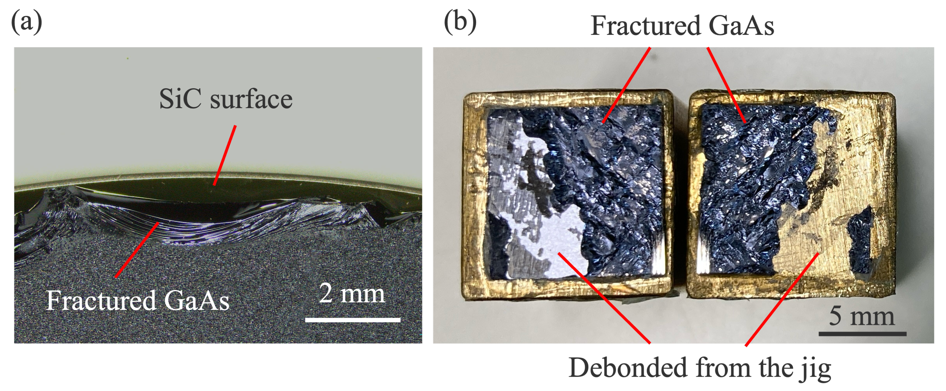
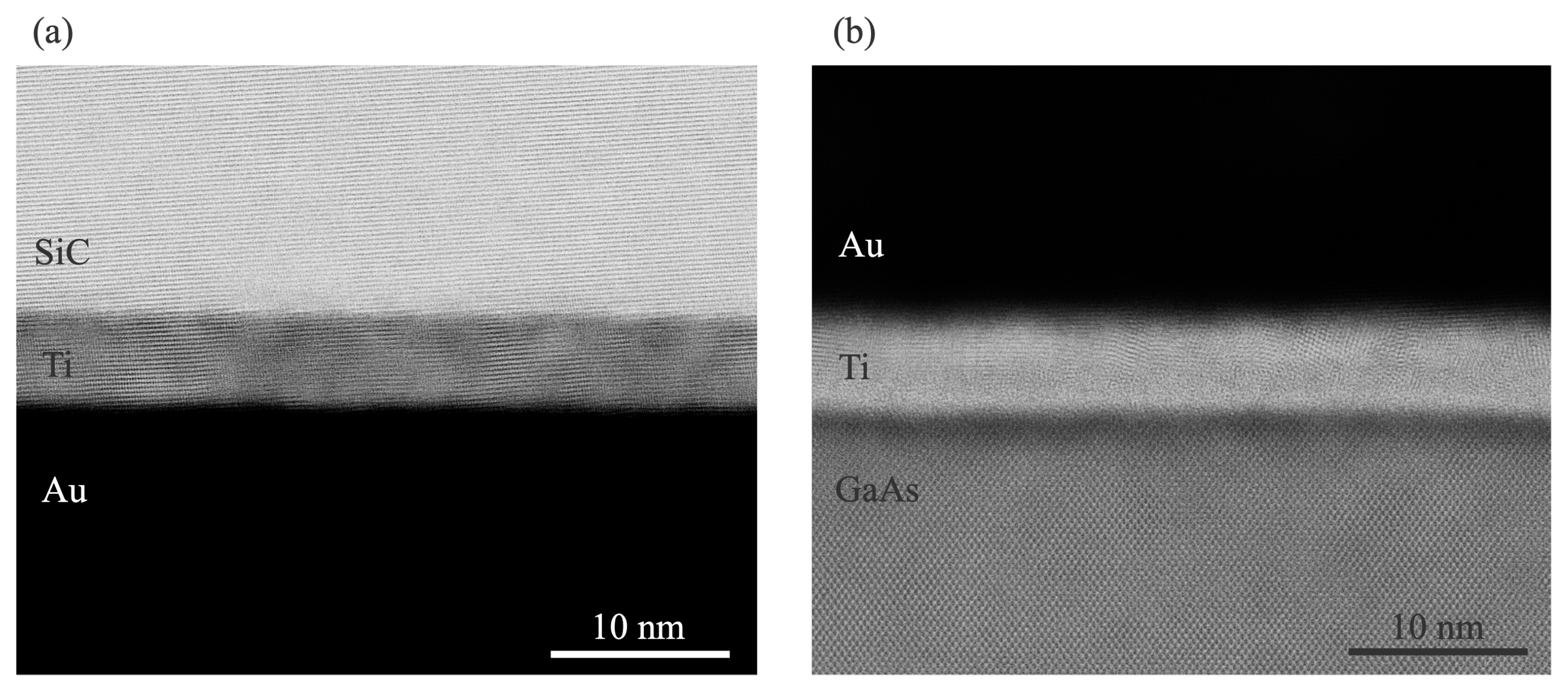
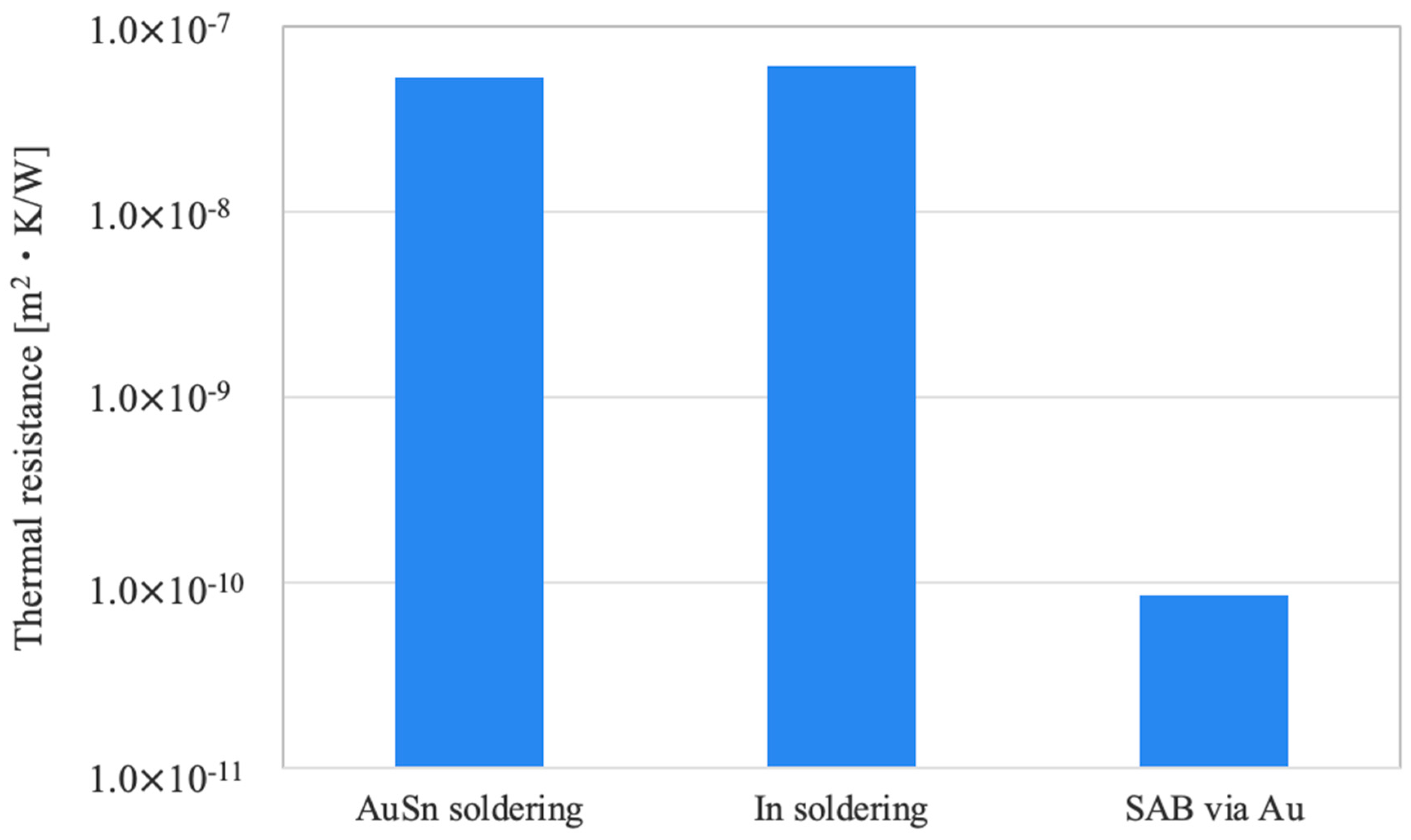
3. Results and Discussion
4. Conclusions
Author Contributions
Funding
Data Availability Statement
Acknowledgments
Conflicts of Interest
References
- Wang, T.; Tian, R.; Zhu, R.; Jiang, L.; Tong, C.; Lu, H.; Song, Y.; Zhang, P. Improved underwater wireless optical communication using a passively mode-locked VECSEL. Opt. Commun. 2023, 547, 129850. [Google Scholar] [CrossRef]
- Tian, R.; Wang, T.; Shen, X.; Zhu, R.; Jiang, L.; Lu, Y.; Lu, H.; Song, Y.; Zhang, P. 108 m Underwater Wireless Optical Communication Using a 490 nm Blue VECSEL and an AOM. Sensors 2024, 24, 2609. [Google Scholar] [CrossRef] [PubMed]
- Voigt, F.F.; Emaury, F.; Bethge, P.; Waldburger, D.; Link, S.M.; Carta, S.; van der Bourg, A.; Helmchen, F.; Keller, U. Multiphoton in vivo imaging with a femtosecond semiconductor disk laser. Biomed. Opt. Express 2017, 8, 3213–3231. [Google Scholar] [CrossRef]
- Nechay, K.; Perttilä, R.; Essaulova, A.; Uusimaa, P. High-power VECSEL with intracavity UV generation for flow cytometry applications. In Proceedings of the High-Speed Biomedical Imaging and Spectroscopy IX, San Francisco, CA, USA, 12 March 2024; Tsia, K.K., Goda, K., Eds.; International Society for Optics and Photonics, SPIE: Bellingham, WA, USA, 2024; Volume 12853, p. 1285306. [Google Scholar] [CrossRef]
- Bondaz, T.A.G.; McInerney, J.G.; Moloney, J.V.; Jones, R.J. Broadband 1.5 GHz VECSEL-Based Laser System for High Speed Multicontrast Nonlinear Imaging. IEEE Photonics Technol. Lett. 2023, 35, 589–592. [Google Scholar] [CrossRef]
- Herper, M.; Gronenborn, S.; Gu, X.; Kolb, J.; Miller, M.; Moench, H. VECSEL for 3D LiDAR applications. In Proceedings of the Vertical External Cavity Surface Emitting Lasers (VECSELs) IX, San Francisco, CA, USA, 4 March 2019; Keller, U., Ed.; International Society for Optics and Photonics, SPIE: Bellingham, WA, USA, 2019; Volume 10901, p. 109010N. [Google Scholar] [CrossRef]
- Korpijärvi, V.M.; Kantola, E.L.; Leinonen, T.; Isoaho, R.; Guina, M. Monolithic GaInNAsSb/GaAs VECSEL Operating at 1550 nm. IEEE J. Sel. Top. Quantum Electron. 2015, 21, 480–484. [Google Scholar] [CrossRef]
- Guina, M.; Rantamäki, A.; Härkönen, A. Optically pumped VECSELs: Review of technology and progress. J. Phys. D Appl. Phys. 2017, 50, 383001. [Google Scholar] [CrossRef]
- Heinen, B.; Zhang, F.; Sparenberg, M.; Kunert, B.; Koch, M.; Stolz, W. On the Measurement of the Thermal Resistance of Vertical-External-Cavity Surface-Emitting Lasers (VECSELs). IEEE J. Quantum Electron. 2012, 48, 934–940. [Google Scholar] [CrossRef]
- Maclean, A.J.; Kemp, A.J.; Hopkins, J.M.; Hastie, J.E.; Giet, S.; Calvez, S.; Dawson, M.D.; Burns, D.; Kim, J.Y.; Kim, K.S.; et al. An analysis of power scaling and thermal management in a 1060 nm VECSEL with a diamond heatspreader. In Proceedings of the 2006 Conference on Lasers and Electro-Optics and 2006 Quantum Electronics and Laser Science Conference, Long Beach, CA, USA, 21–26 May 2006; pp. 1–2. [Google Scholar] [CrossRef]
- Rantamäki, A.; Lindfors, J.; Silvennoinen, M.; Kontio, J.; Tavast, M.; Okhotnikov, O.G. Low Temperature Gold-to-Gold Bonded Semiconductor Disk Laser. IEEE Photonics Technol. Lett. 2013, 25, 1062–1065. [Google Scholar] [CrossRef]
- Baumgärtner, S.; Kahle, H.; Bek, R.; Schwarzbäck, T.; Jetter, M.; Michler, P. Comparison of AlGaInP-VECSEL gain structures. J. Cryst. Growth 2015, 414, 219–222. [Google Scholar] [CrossRef]
- Mangold, M.; Wittwer, V.J.; Sieber, O.D.; Hoffmann, M.; Krestnikov, I.L.; Livshits, D.A.; Golling, M.; Südmeyer, T.; Keller, U. VECSEL gain characterization. Opt. Express 2012, 20, 4136–4148. [Google Scholar] [CrossRef]
- Gbele, K.; Laurain, A.; Hader, J.; Stolz, W.; Moloney, J.V. Design and Fabrication of Hybrid Metal Semiconductor Mirror for High-Power VECSEL. IEEE Photonics Technol. Lett. 2016, 28, 732–735. [Google Scholar] [CrossRef]
- Sheikhi, R.; Huo, Y.; Shi, F.G.; Lee, C.C. Low Temperature VECSEL-to-Diamond Heterogeneous Integration with Ag-In Spinodal Nanostructured Layer. Scr. Mater. 2021, 194, 113628. [Google Scholar] [CrossRef]
- Lyytikäinen, J.; Rautiainen, J.; Sirbu, A.; Mereuta, A.; Caliman, A.; Kapon, E.; Okhotnikov, O. Wafer fused InP-GaAs optically pumped semiconductor disk laser operating at 1.57 μm. In Proceedings of the Photon Counting Applications, Quantum Optics, and Quantum Information Transfer and Processing II, Prague, Czech Republic, 18 May 2009; Dusek, M., Prochazka, I., Sobolewski, R., Eds.; International Society for Optics and Photonics, SPIE: Bellingham, WA, USA, 2009; Volume 7355, p. 73550C. [Google Scholar] [CrossRef]
- Ho, C.Y.; Powell, R.W.; Liley, P.E. Thermal Conductivity of the Elements. J. Phys. Chem. Ref. Data 1972, 1, 279–421. [Google Scholar] [CrossRef]
- Inyushkin, A.V.; Taldenkov, A.N.; Ralchenko, V.G.; Bolshakov, A.P.; Koliadin, A.V.; Katrusha, A.N. Thermal conductivity of high purity synthetic single crystal diamonds. Phys. Rev. B 2018, 97, 144305. [Google Scholar] [CrossRef]
- Levinshtein, M.E.; Rumyantsev, S.L.; Shur, M.S. Properties of Advanced Semiconductor Materials: GaN, AIN, InN, BN, SiC, SiGe; John Wiley & Sons: Hoboken, NJ, USA, 2001. [Google Scholar]
- Li, X.; Jiang, K.; Zhu, Z.; Su, J.; Xia, W.; Xu, X. High-brightness 808 nm semiconductor laser diode packaged by SiC heat sink. J. Mod. Opt. 2020, 67, 1017–1021. [Google Scholar] [CrossRef]
- Apollonov, V.V.; Babayants, G.I.; Gruden’, M.N.; Derzhavin, S.I.; Kazakov, A.A.; Kishmakhov, B.S.; Koval’, Y.P.; Kuz’minov, V.V.; Mashkovskii, D.A.; Prokhorov, A.M.; et al. Investigation of the thermal properties of a laser-diode linear array on a silicon carbide heat sink. Quantum Electron. 1997, 27, 845. [Google Scholar] [CrossRef]
- Giet, S.; Kemp, A.J.; Burns, D.; Calvez, S.; Dawson, M.D.; Suomalainen, S.; Harkonen, A.; Guina, M.; Okhotnikov, O.; Pessa, M. Comparison of thermal management techniques for semiconductor disk lasers. In Proceedings of the Solid State Lasers XVII: Technology and Devices, San Jose, CA, USA, 14 February 2008; Clarkson, W.A., Hodgson, N., Shori, R.K., Eds.; International Society for Optics and Photonics, SPIE: Bellingham, WA, USA, 2008; Volume 6871, p. 687115. [Google Scholar] [CrossRef]
- Gallery, J.; Lytwynec, S. AuSn Preform Thickness’s Effect on Thermal Management in Semiconductor Laser Applications. IMAPSource Proc. 2023, 2023, 5–10. [Google Scholar] [CrossRef]
- Higurashi, E.; Okumura, K.; Nakasuji, K.; Suga, T. Surface activated bonding of GaAs and SiC wafers at room temperature for improved heat dissipation in high-power semiconductor lasers. Jpn. J. Appl. Phys. 2015, 54, 030207. [Google Scholar] [CrossRef]
- Takeuchi, K.; Fujino, M.; Matsumoto, Y.; Suga, T. Room temperature bonding and debonding of polyimide film and glass substrate based on surface activate bonding method. Jpn. J. Appl. Phys. 2018, 57, 02BB05. [Google Scholar]
- Takeuchi, K.; Mu, F.; Matsumoto, Y.; Suga, T. Room Temperature Wafer Bonding of Glass Using Aluminum Oxide Intermediate Layer. Adv. Mater. Interfaces 2021, 8, 2001741. [Google Scholar] [CrossRef]
- Takeuchi, K.; Suga, T. Quantification of wafer bond strength under controlled atmospheres. Jpn. J. Appl. Phys. 2022, 61, SF1010. [Google Scholar] [CrossRef]
- Tsau, C.; Spearing, S.; Schmidt, M. Fabrication of wafer-level thermocompression bonds. J. Microelectromech. Syst. 2002, 11, 641–647. [Google Scholar] [CrossRef]
- Taklo, M.M.V.; Storås, P.; Schjølberg-Henriksen, K.; Hasting, H.K.; Jakobsen, H. Strong, high-yield and low-temperature thermocompression silicon wafer-level bonding with gold. J. Micromech. Microeng. 2004, 14, 884. [Google Scholar] [CrossRef]
- Yamamoto, M.; Matsumae, T.; Kurashima, Y.; Takagi, H.; Suga, T.; Itoh, T.; Higurashi, E. Comparison of Argon and Oxygen Plasma Treatments for Ambient Room-Temperature Wafer-Scale Au–Au Bonding Using Ultrathin Au Films. Micromachines 2019, 10, 119. [Google Scholar] [CrossRef] [PubMed]
- Takeuchi, K.; Wang, J.; Kim, B.; Suga, T.; Higurashi, E. Room temperature bonding of Au assisted by self-assembled monolayer. Appl. Phys. Lett. 2023, 122, 051603. [Google Scholar] [CrossRef]
- Higurashi, E.; Okumura, K.; Kunimune, Y.; Saga, T.; Hagiwara, K. Room-Temperature Bonding of Wafers with Smooth Au Thin Films in Ambient Air Using a Surface-Activated Bonding Method. IEICE Trans. Electron. 2017, E100.C, 156–160. [Google Scholar] [CrossRef]
- Takeuchi, K.; Koseki, S.; Thu, L.H.H.; Matsumae, T.; Takagi, H.; Kurashima, Y.; Tsuda, T.; Tokuhisa, T.; Shimizu, T.; Higurashi, E. Room temperature bonding of Au plating through surface smoothing using polyimide template stripping. Sens. Actuators A Phys. 2025, 383, 116211. [Google Scholar] [CrossRef]
- Messmer, C.; Bilello, J.C. The surface energy of Si, GaAs, and GaP. J. Appl. Phys. 1981, 52, 4623–4629. [Google Scholar] [CrossRef]
- Yu, C.; Yang, D.; Zhao, D.; Sheng, Z. Reliability of nano-silver soldering paste with high thermal conductivity. In Proceedings of the 2019 20th International Conference on Electronic Packaging Technology (ICEPT), Hong Kong, China, 12–15 August 2019; pp. 1–4. [Google Scholar] [CrossRef]
- Zhao, S.; Yang, X.; Wu, X.; Liu, G. Investigation on Creep-Fatigue Interaction Failure of Die-Attach Solder Layers in IGBTs Under Power Cycling. IEEE Trans. Power Electron. 2025, 40, 7261–7274. [Google Scholar] [CrossRef]

Disclaimer/Publisher’s Note: The statements, opinions and data contained in all publications are solely those of the individual author(s) and contributor(s) and not of MDPI and/or the editor(s). MDPI and/or the editor(s) disclaim responsibility for any injury to people or property resulting from any ideas, methods, instructions or products referred to in the content. |
© 2025 by the authors. Licensee MDPI, Basel, Switzerland. This article is an open access article distributed under the terms and conditions of the Creative Commons Attribution (CC BY) license (https://creativecommons.org/licenses/by/4.0/).
Share and Cite
Takeuchi, K.; Higurashi, E. Wafer Bonding of GaAs and SiC via Thin Au Film at Room Temperature. Micromachines 2025, 16, 439. https://doi.org/10.3390/mi16040439
Takeuchi K, Higurashi E. Wafer Bonding of GaAs and SiC via Thin Au Film at Room Temperature. Micromachines. 2025; 16(4):439. https://doi.org/10.3390/mi16040439
Chicago/Turabian StyleTakeuchi, Kai, and Eiji Higurashi. 2025. "Wafer Bonding of GaAs and SiC via Thin Au Film at Room Temperature" Micromachines 16, no. 4: 439. https://doi.org/10.3390/mi16040439
APA StyleTakeuchi, K., & Higurashi, E. (2025). Wafer Bonding of GaAs and SiC via Thin Au Film at Room Temperature. Micromachines, 16(4), 439. https://doi.org/10.3390/mi16040439