Article

Low-Pressure Chemical Vapor Deposition SiNx Process Study and Its Impact on Interface Characteristics of AlGaN/GaN MISHEMTs

Institute of Next Generation Semiconductor Materials, Southeast University, Suzhou 215123, China
*
Author to whom correspondence should be addressed.
Micromachines 2025, 16(4), 442; https://doi.org/10.3390/mi16040442
Submission received: 24 March 2025 / Revised: 6 April 2025 / Accepted: 7 April 2025 / Published: 9 April 2025
(This article belongs to the Special Issue GaN-Based Materials and Devices: Research and Applications)

Abstract

:
This study employed low-pressure chemical vapor deposition (LPCVD) SiNx as both the gate dielectric layer and surface passivation layer, systematically investigating the effects of different growth conditions on the dielectric layer quality, two-dimensional electron gas (2DEG) characteristics, interface trap density, and devices’ performance, thereby optimizing the growth parameters of LPCVD SiNx. The experiment investigated the effects of growth parameters such as the growth temperature, chamber pressure, and gas flow ratio on the growth rate of SiNx during the process of growing SiNx using the LPCVD technique. Further studies were performed to analyze the impact of SiNx introduction on the 2DEG performance. The results indicated that both Si-rich and N-rich SiNx compositions could enhance the 2DEG density improvement induced by SiNx passivation. The impact of the gas flow ratio on the interface trap density is studied. Through the quantitative characterization of the interface trap density using the pulse-mode IDS-VGS method and frequency-dependent capacitance–voltage (C-V) measurement, the results show that the interface trap density decreases with an increased Si-to-N ratio.

1. Introduction

Gallium nitride (GaN) has emerged as a highly sought-after material in the research domain of semiconductor devices, owing to its remarkable characteristics such as a high electron saturation velocity, wide bandgap, high critical breakdown field strength, and high operating temperature [1]. AlGaN/GaN high-electron-mobility transistors (HEMTs) based on GaN materials have demonstrated dominant performance in high-frequency and high-voltage applications [2]. However, during HEMT operation, the “virtual gate” effect formed at the AlGaN surface can deplete portions of the channel two-dimensional electron gas (2DEG), leading to reduced device output current and current collapse. To mitigate the adverse effects of the “virtual gate” phenomenon while suppressing the gate leakage current and enhancing gate swing, depositing a material layer on the AlGaN surface as both a passivation layer and gate dielectric has been widely studied [3].
At present, the surface passivation of AlGaN has been extensively studied. A series of materials have been used as passivation layers and dielectric layers for GaN MISHEMT devices, including but not limited to Al2O3, SiO2, HfO2, SiNx, etc. [4,5,6,7]. Among a wide variety of passivation materials, SiNx, due to its unique properties, has become the most commonly used passivation material for GaN HEMTs in industry. SiNx has been prepared by several techniques, including plasma-enhanced chemical vapor deposition (PECVD) [8], metal–organic chemical vapor deposition (MOCVD) [9,10], and low-pressure chemical vapor deposition (LPCVD) [11,12]. Each of these techniques has its own unique process parameters and applicable scenarios, providing diverse options for the effective application of SiNx in GaN MISHEMT devices. In recent years, LPCVD SiNx has been widely used in AlGaN/GaN MISHEMTs as gate dielectric and surface passivation layers. Hua et al. used LPCVD to deposit SiNx films at 780 °C as the gate dielectrics of AlGaN/GaN MISHEMTs [13]. Liu et al. deposited 20 nm LPCVD SiNx at 650 °C as the gate dielectric, achieving high on–off current ratios and high breakdown voltages [14]. Although SiNx prepared by LPCVD has been proven to be suitable for use as gate dielectric and passivation layers in AlGaN/GaN MISHEMTs, it has also been reported that the insertion of such a gate dielectric layer leads to a high density of traps at the interface between the SiNx dielectric layer and the III-nitride. The charging and discharging behavior of these interface traps during device operation can have an adverse impact on the device’s performance and stability [15].
In this paper, we focus on LPCVD SiNx, comparing the effects of different growth parameters on the SiNx growth rate and investigating the impacts of SiNx films with varying qualities on 2DEG characteristics. Based on the influence of SiNx grown under different gas flow ratios on the 2DEG density, a detailed analysis is conducted to explore the underlying mechanisms responsible for the SiNx-induced increase in the 2DEG density. The pulse-mode IDS-VGS method and the frequency-dependent C-V method were employed to characterize the interface traps quantitatively. Its impact on AlGaN/GaN MISHEMT devices’ performance is also reported.

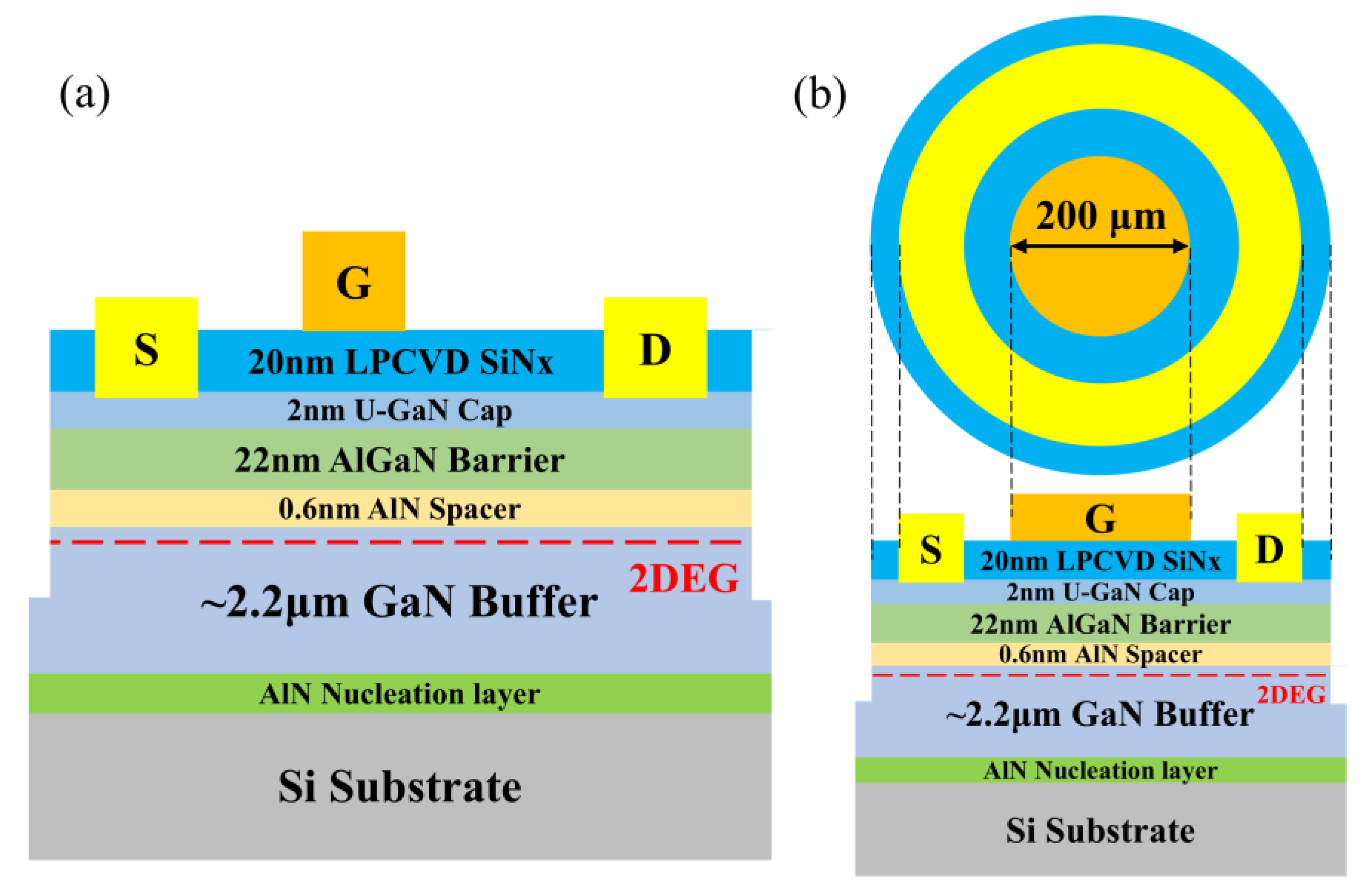
2. Materials and Methods

The AlGaN/GaN HEMT structure was grown on a 6-inch Si (111) substrate via MOCVD by Suzhou Hanhua Ltd., Suzhou, China. The epitaxial structure, from bottom to top, consisted of an AlN nucleation layer, a 1.8 μm high-resistivity AlGaN/GaN buffer layer, a 350 nm GaN channel layer, a 0.6 nm AlN insertion layer, a 22 nm AlGaN barrier layer, and a 2 nm GaN cap layer. Finally, the grown wafer was divided into multiple samples, which were then cleaned and placed in an LPCVD system to deposit SiNx under different growth conditions. Inductively Coupled Plasma Etching (ICP) technology was employed to perform dry etching on the unprotected SiNx and III-nitride to achieve mesa isolation. After the mesa isolation process was completed, dry etching was utilized again to precisely open the ohmic contact areas defined by the second photolithography mask. Subsequently, an ohmic metal layer composed of Ti/Al/Ni/Au with thicknesses of 20 nm, 130 nm, 50 nm, and 50 nm, respectively, was deposited by electron beam evaporation. Thereafter, the samples were placed in a N2 atmosphere at 850 °C for a 30 s rapid annealing treatment. The contact resistance of the ohmic contact was accurately measured using the Transmission Line Model (TLM) method, and the measured value was 0.55 Ω·cm2. Through comparative analysis, this measured value was found to be at a comparable level to the data reported in the previous literature [16,17]. In the final stage of device fabrication, the gate region was patterned using the third photolithography mask, and then a gate metal layer of Ni/Al with thicknesses of 50 nm and 500 nm, respectively, was deposited by electron beam evaporation. For the fabricated device, the gate length was set to 2 μm, the gate width was 100 μm, the distance between the gate and the source was 2 μm, and the distance between the gate and the drain was 11 μm. Figure 1 depicts the schematic diagrams of the fabricated LPCVD SiNx/AlGaN/GaN MISHEMT and MIS diode.
To characterize the quality of the LPCVD SiNx, the thickness and refractive index of SiNx were determined using a spectroscopic ellipsometer. The microtopography of the samples was observed, and the surface roughness after SiNx growth was measured by atomic force microscopy (AFM) with a scanning range of 5 μm × 5 μm. The 2DEG properties including the 2DEG density, mobility, and sheet resistance were measured at room temperature via the Van der Pauw Hall measurement method using a Hall effect tester (HL9900, Toho, Nagoya, Japan). Additionally, the Keithley 4200 semiconductor parameter analyzer (Keithley 4200A-SCS, Tektronix, Beaverton, OR, USA) was employed to evaluate the electrical performance of the MISHEMTs and characterize the interface state density at the gate dielectric/III-nitride interface.

3. Results

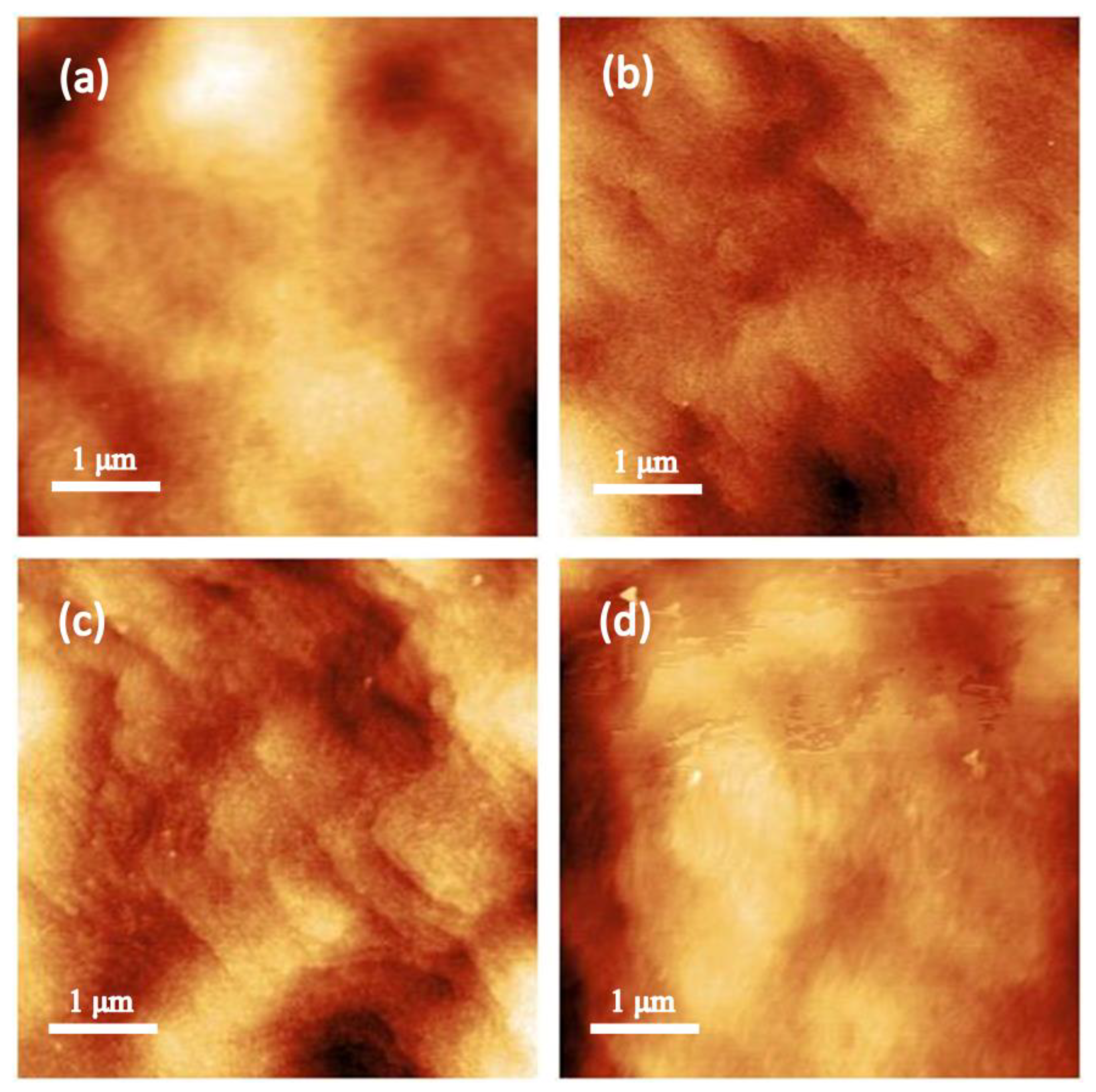
3.1. Modulation of LPCVD SiNx Growth Conditions

The quality of LPCVD SiNx films is primarily governed by three growth parameters: the growth temperature (T), chamber pressure (P), and reactant gas flow ratio (SiH2Cl2 (DCS)/NH₃). The relationship between the deposition rate and these parameters was systematically investigated. Figure 2a illustrates the SiNx deposition rate as a function of the growth temperature. Over the temperature range from 760 °C to 795 °C, the deposition rate increased monotonically due to the enhanced decomposition efficiency and reactivity of the DCS and NH3 precursors, which accelerated chemical reactions on the AlGaN surface. However, further temperature elevation (795 °C to 840 °C) resulted in a decline in the deposition rate, most likely attributed to the premature gas-phase decomposition of precursors that reduced the availability of reactive species for film formation [18]. Figure 2b demonstrates a direct proportionality between the SiNx deposition rate and the gas flow ratio. As shown in Figure 2c, a similar positive correlation exists between the deposition rate and the chamber pressure, consistent with prior research findings [18,19].
The refractive index is a critical metric for evaluating the quality of LPCVD SiNx films. To investigate the relationship between the quality of SiNx and the growth parameters, the refractive index of the aforementioned samples was measured. Figure 2 illustrates the dependence of the SiNx refractive index on the temperature, pressure, and gas flow ratio, with the gas flow ratio exhibiting the most significant influence. To further investigate the influence of the SiNx growth parameters on the characteristics of the 2DEG, seven samples with SiNx layers of different qualities grown by LPCVD were selected for subsequent research. Meanwhile, a sample without SiNx was chosen as a reference sample. All these seven samples were taken from the same epitaxial wafer. The specific growth parameters are summarized in Table 1.

3.2. Influence of LPCVD SiNx Growth Conditions on 2DEG

The 2DEG density (Ns), sheet resistance (Rs), and electron mobility (µn) results of Samples A, B, C, D, E, F, and G are presented in Table 1. Compared with the sample without a SiNx dielectric layer, a significant enhancement in the 2DEG density was observed in samples with deposited SiNx. Some viewpoints hold that the introduction of the passivation layer leads to an enhancement in the piezoelectric polarization effect caused by the additional strain in the AlGaN barrier layer and the entry of ionized electrons from Si donors into the channel, which results in an increase in the 2DEG density [20,21]. It has been reported that the diffusion of Si can only be achieved under high-temperature conditions [21,22]. To validate the above hypothesis, three epitaxial wafers were used as samples to investigate the changes in the 2DEG density before and after SiNx growth via PECVD. The SiNx growth conditions were consistent for all three samples. The Ns, Rs, and µn results are shown in Table 2. Consistent with the LPCVD SiNx outcomes, samples with PECVD SiNx exhibited significant 2DEG density increases. However, the high-energy ions in the PECVD process damage the surface of AlGaN/GaN, leading to an increase in defects. These defects increase the scattering of carriers, which in turn results in a decrease in electron mobility [23]. The experimental results show that depositing SiNx under low-temperature conditions can also increase the 2DEG density, indicating that the entry of ionized electrons from Si donors into the channel is not the main reason for the increase in the 2DEG density. By observing the 2DEG density results of Samples A, B, C, and D, it can be found that as the gas flow ratio increases, the 2DEG density in the AlGaN/GaN heterojunction channel gradually increases. However, Sample E does not seem to follow this rule. Its Ns reaches 0.84 × 1013 cm−2, which is higher than that of Sample A. Strain relaxation typically leads to the formation of defects such as dislocations and reduces the interface quality. Nevertheless, some studies have pointed out that appropriate strain relaxation may release local stress and, in turn, increase Ns [10,24].
Two different conclusions prove that the strain variation is not the main cause of the increase in the 2DEG concentration. Siddique et al. found that N-rich SiNx has a lower dielectric constant (ε), which leads to a decrease in the surface potential at the interface. The decrease in the surface potential makes the ionization energy closer to the Fermi level (EF), thereby promoting the ionization of surface states and increasing the 2DEG density [25]. Meanwhile, for Si-rich SiNx, the reduction in the proportion of NH3 introduces more un-nitrided Ga dangling bonds, forming near-conduction-band states. This results in a decrease in the surface potential and an enhanced accumulation of 2DEG concentration [26]. Therefore, the decrease in the surface potential is the main cause of the increase in the 2DEG concentration. Compared with Sample B, the growth temperature of Sample F was reduced by 15 °C, resulting in moderate reductions in both Ns and µn, while Rs correspondingly increased. Considering the effects of the two temperatures on the growth rate, this study concludes that SiNx deposited under the 795 °C condition exhibits superior quality compared to the 780 °C deposition condition. Upon comparing the results of Samples B and G, it was found that variations in pressure had little influence on Ns.
Table 1 demonstrates that the introduction of LPCVD SiNx also exerted a significant influence on both µn and Rs. After SiNx deposition, notable enhancements were observed in µn, accompanied by corresponding improvements in Rs. The analysis of Samples A–D reveals that increasing the gas flow ratio during LPCVD SiNx growth led to a gradual rise in µn from 1822 cm2/V∙s to 1992 cm2/V∙s, while Rs decreased from 496 Ω/□ to 373 Ω/□. These results demonstrate that optimizing the gas flow ratio in the LPCVD SiNx process can effectively enhance the transport properties of the 2DEG channel.
The experimental results demonstrate that the gas flow ratio during LPCVD SiNx growth exerts a significant impact on both the SiNx film quality and 2DEG characteristics in the channel. To further investigate the influence of the gas flow ratio on the interface trap density and device electrical performance, Samples A, B, and C were selected for subsequent device studies. The SiNx films prepared under three different gas flow ratios are in N-rich, standard Si/N ratio, and Si-rich states, respectively. Figure 3 shows the 5 μm × 5 μm AFM images of the AlGaN/GaN HEMT surface. Figure 3d is the AFM image of the unpassivated surface, with an AFM root mean square (RMS) roughness of 1.84 nm. Figure 3a–c are the AFM images of the passivated surfaces. The gas flow ratios (DCS/NH3) of Samples A-C are 1:8, 1:4, and 1:1, respectively, and their RMS roughness values are 1.36 nm, 1.55 nm, and 1.56 nm, respectively.

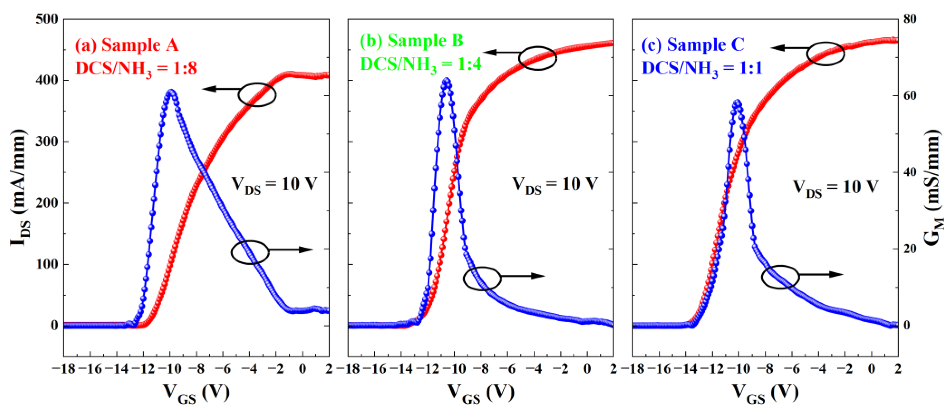
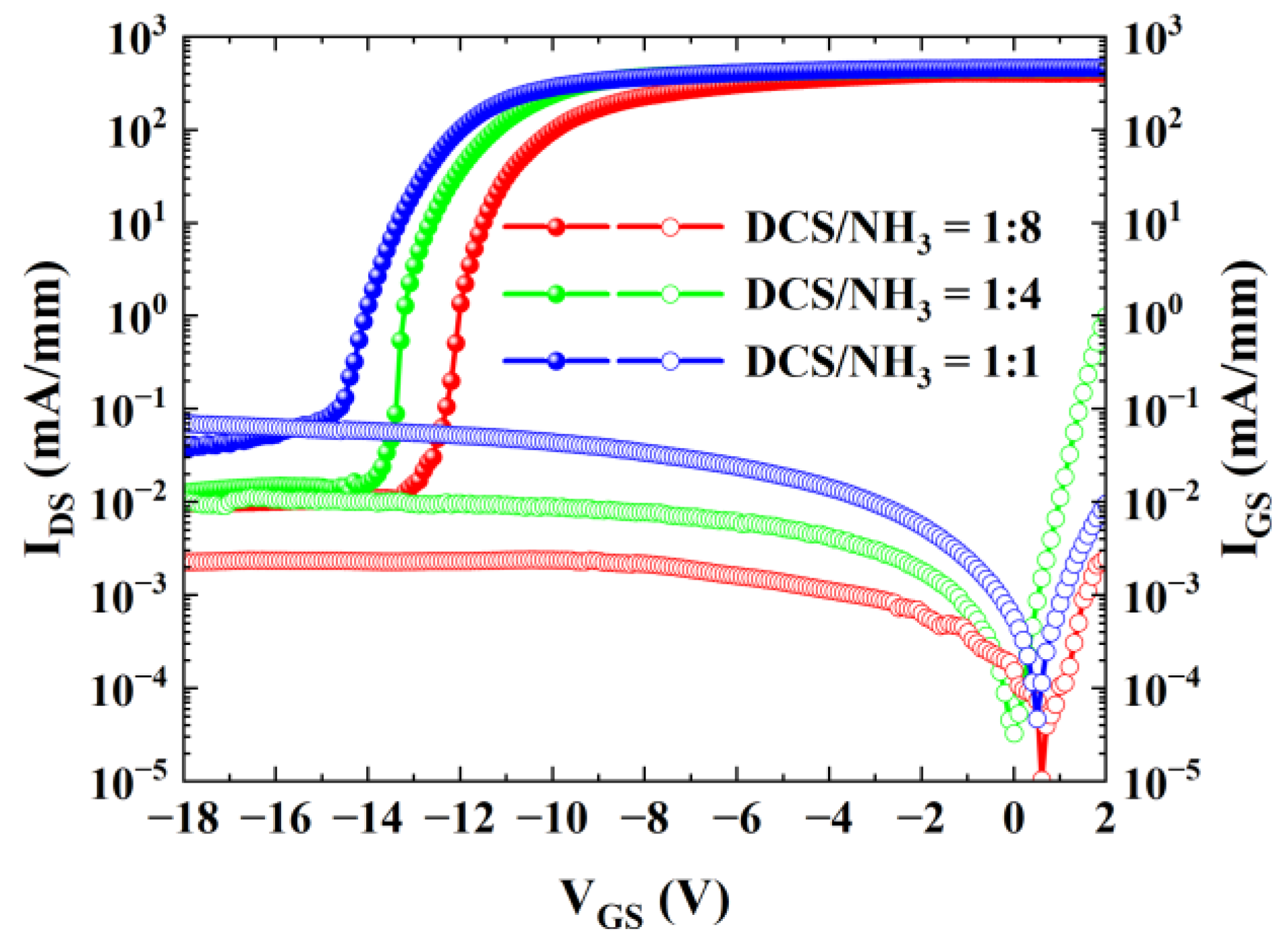
3.3. DC Characteristics of Devices

Figure 4 and Figure 5 present the output and transfer characteristics of the AlGaN/GaN MISHEMTs under DC conditions. The dimensions of the devices involved are WG/LG/LGS/LGD = 100/2/2/11 μm. In the test depicted in Figure 4, the output curves of the devices are plotted from bottom to top, corresponding to gate voltages ranging from −16 V to 4 V with a step of 2 V. Figure 5 depicts the transfer characteristics of the three samples. In this measurement, the drain–source voltage VDS was set at 10 V, and the gate–source voltage VGS was scanned from −18 V to 2 V. The threshold voltages of Sample A, Sample B, and Sample C are −12.1 V, −13.2 V, and −13.4 V, respectively. It should be noted that while the set target thickness of SiNx is identical, the samples are processed at different growth runs, which might cause some thickness difference which may be responsible for the Vth fluctuation mentioned above. It is believed that as the thickness of SiNx increases, the threshold voltage exhibits a negative shift. Notably, in accordance with the research findings of Zhu et al. [26], the minor variations in the SiNx thickness across different samples do not exert a significant influence on the interface trap density of AlGaN/GaN MISHEMTs. Moreover, there are no discernible differences in the peak transconductance (GM), which remains approximately 60 mS/mm for all samples.
Figure 6 presents the capacitance–voltage (C-V) characteristic curves of AlGaN/GaN MIS diodes with three different gas flow ratios under normal temperature conditions. The gate diameter of these diodes was uniformly 200 μm. During the testing process, the gate voltage was first scanned forward from −18 V to 4 V in specific steps and then scanned backward from 4 V to −18 V at a 500 kHz frequency. Through an analysis of the experimental data and curves, it is clear that all three groups of samples exhibit the threshold hysteresis phenomenon, with varying degrees of hysteresis. This hysteresis is primarily attributed to the presence of numerous acceptor-like traps at the interface between the gate dielectric and III-nitride materials [15]. Sample A exhibited the largest hysteresis, while Sample C demonstrated the smallest, indicating that high-refractive-index SiNx effectively reduces traps with long emission time constants at the interface.

3.4. Analysis of Gate Leakage Current

As one of the crucial parameters of GaN HEMT devices, the gate leakage current exerts a vital influence on the device’s performance and reliability. Figure 7 depicts the curves of the drain current and gate current of the three samples as a function of the device gate voltage, with VDS set at 10 V. It can be observed that as the gas flow ratio (DCS/NH3) gradually increases, the gate leakage current of the device exhibits an upward trend. This is primarily attributed to the fact that the increase in the Si source leads to an elevation in the concentration of Si donors at the interface between the dielectric layer and the III-nitride, thereby exacerbating the gate leakage phenomenon [21].

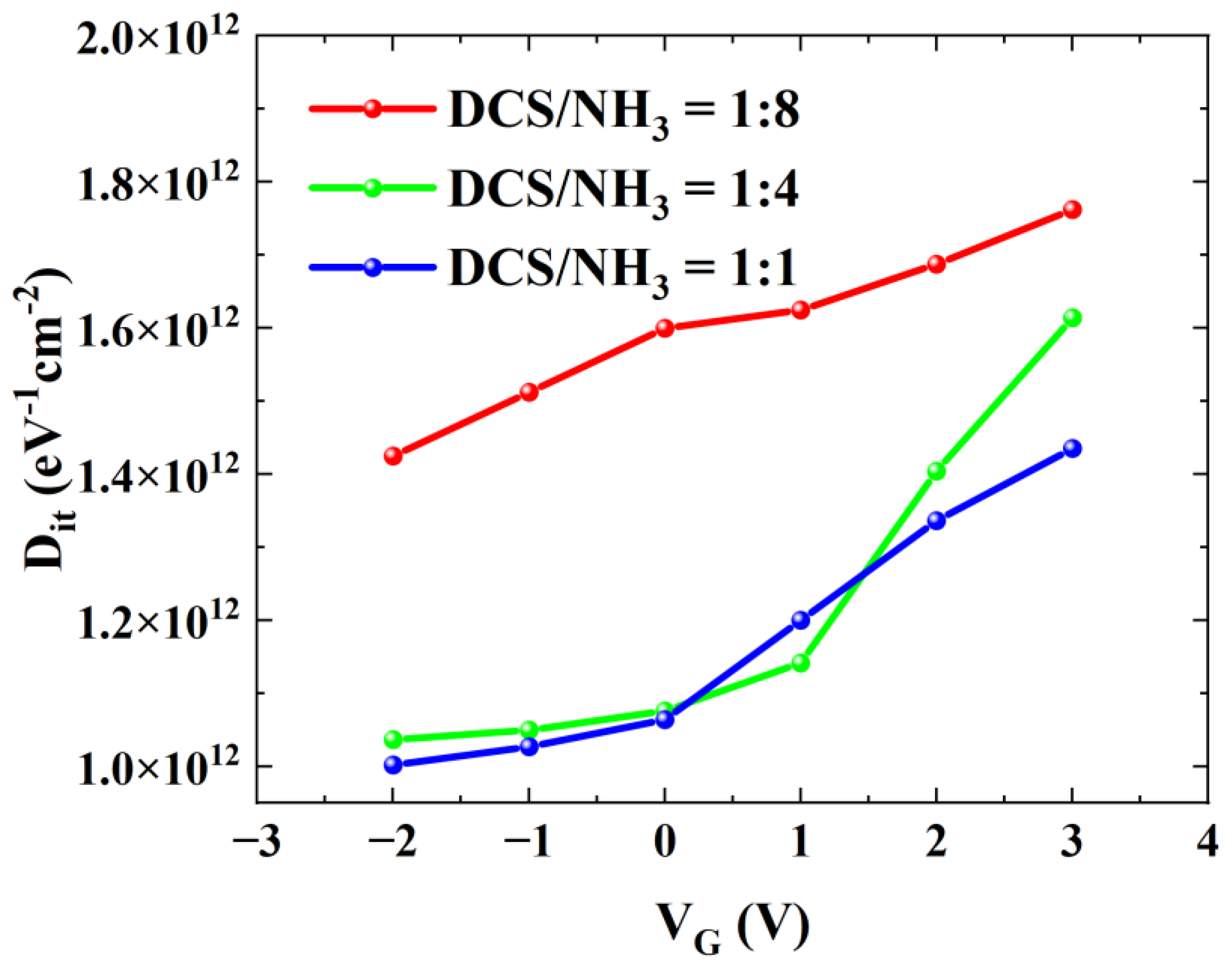
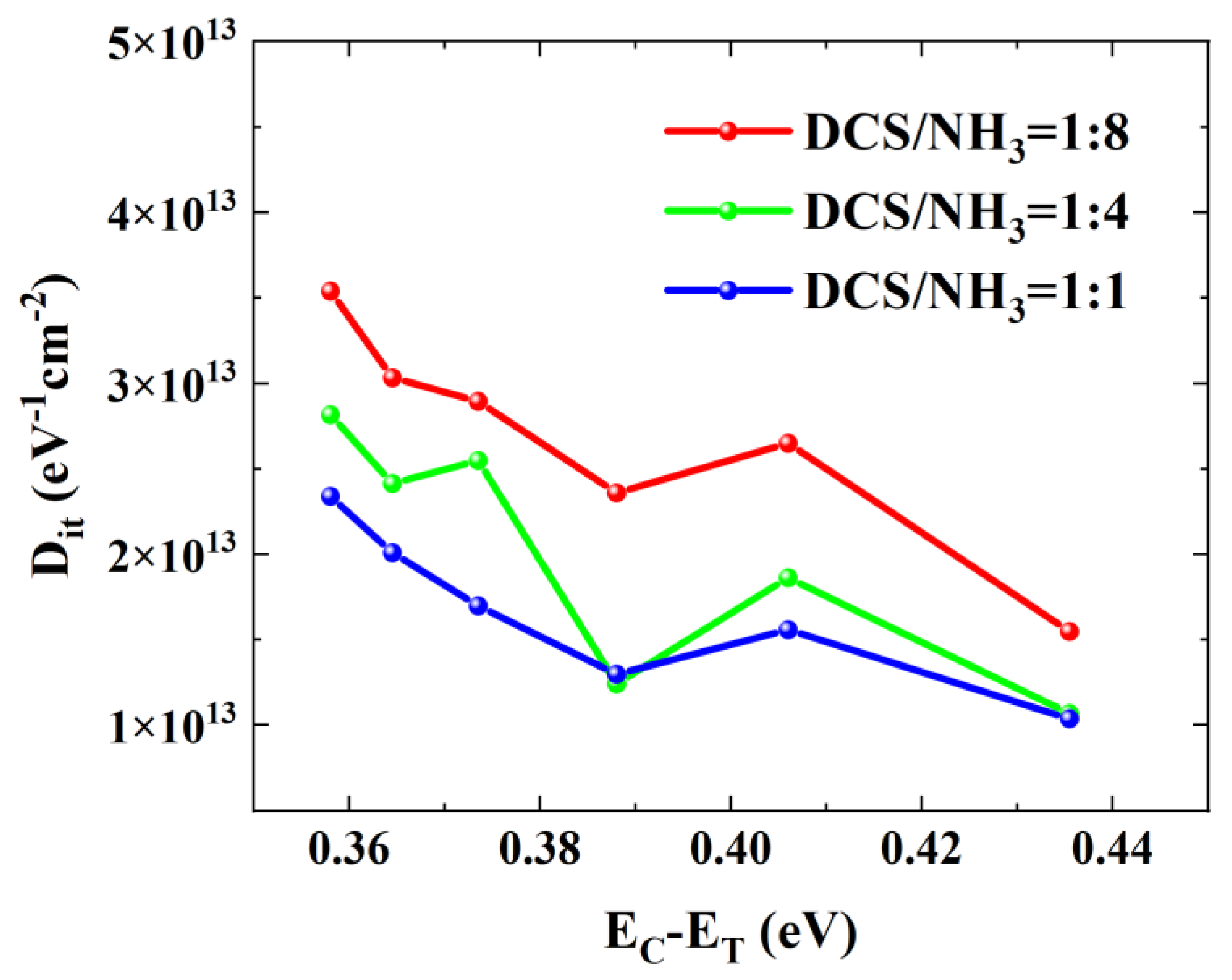
3.5. Interface Trap Characterization

Figure 6 indicates the existence of a large number of traps at the interface between the dielectric layer and III-nitride. To accurately evaluate the interface traps in AlGaN/GaN MISHEMTs and AlGaN/GaN MIS diodes, the pulse-mode IDS-VGS method and the frequency-dependent C-V measurement were employed to characterize and analyze the distribution of interface states.

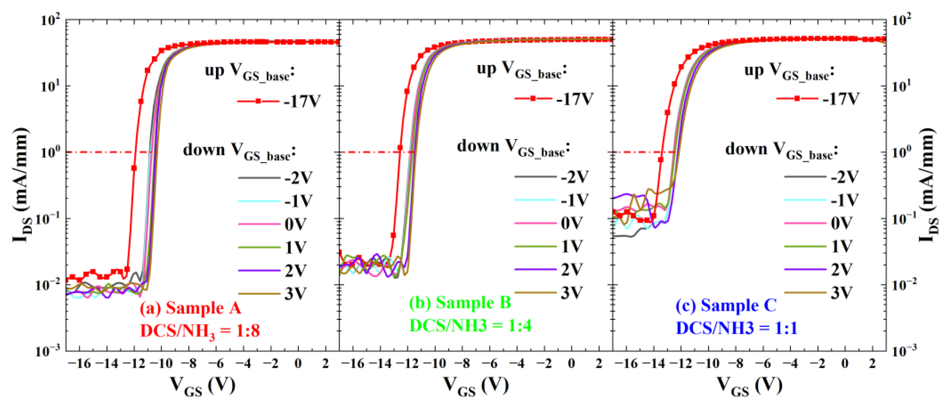
3.5.1. Pulse-Mode IDS-VGS Method

The pulse-mode IDS-VGS method is a common technique for characterizing interface traps in AlGaN/GaN MISHEMTs. In this study, to minimize the impact of the drain bias on the charge–discharge process of interface traps, the drain–source bias VDS was set to 1 V. Figure 8 presents the pulsed-mode double-sweep curves of MISHEMT devices fabricated with three different gas flow ratios. Under the condition of VDS = 1 V, when applying a forward scanning signal to the gate, the quasi-static gate bias voltage VGS_base during forward scanning should be less than the device threshold voltage, thus set to −17 V. The forward sweep utilized a 500 ms period with a 50 μs pulse width and a maximum gate bias of VGS_max = 3 V. For reverse sweeps, the quasi-static bias was typically chosen near the gate voltage where the output current approaches saturation to better characterize interface traps. As shown in Figure 8, the reverse-sweep VGS_base was varied from −2 V to 3 V with a step of 1 V. Based on the difference in the threshold voltages between the forward and reverse scans of devices, the density of interface traps with an electron emission time constant greater than the pulse width can be determined. The density of interface traps Dit can be determined by the following formula:
D it = C OX   ·   Δ V TH q ,
where the COX values of the three samples are 205 nF/cm2 (Sample A), 215 nF/cm2 (Sample B), and 200 nF/cm2 (Sample C), and ∆VTH represents the difference in the threshold voltages between the forward and reverse scans.
The energy level depth (∆ET = EC − ET) corresponding to the electron emission time constant greater than the pulse width can be obtained from the Shockley–Read–Hall statistics [27]:
Δ E T = kTln ( v th σ n N C τ e ) ,
where k is the Boltzmann constant, T is the absolute temperature, vth is the electron thermal velocity, σ n is the electron capture cross-section, and NC is the effective density of states in the GaN conduction band. According to the calculation, under the condition that τ e is 50 μs, ∆ET = 0.438 eV. Therefore, the detectable energy range in this experiment is EC − ET ≥ 0.438 eV.
Figure 9 illustrates the interface trap density Dit extracted from the three samples under different reverse-scan VGS_base. When the reverse-scan VGS_base is set to 3 V, the values of Sample A, Sample B, and Sample C are 1.76 × 10¹² eV−1·cm−2, 1.61 × 10¹² eV−1·cm−2, and 1.44 × 10¹² eV−1·cm−2, respectively. The results indicate that as the value of the DCS/NH₃ ratio increases, the interface state density of the MISHEMT device gradually decreases. This is consistent with the results of the C-V measurements of the AlGaN/GaN MIS diodes presented previously.

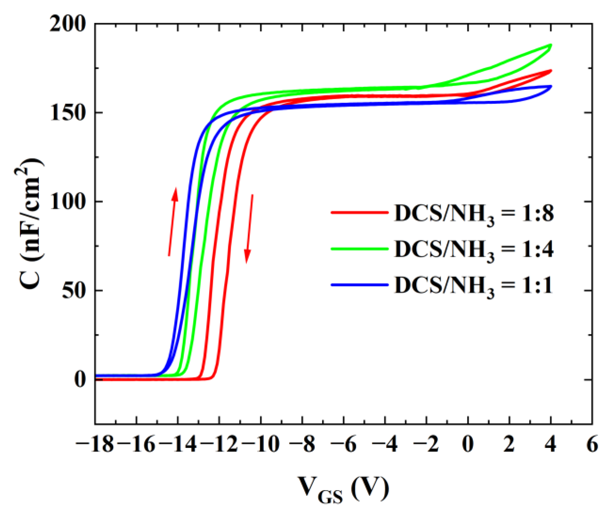
3.5.2. Frequency-Dependent C-V Measurement

While the pulse-mode IDS-VGS method can characterize the interface state density in AlGaN/GaN MISHEMT devices, the presence of drain bias induces the partial detrapping of electrons from interface traps, leading to underestimated interface state density measurements. To achieve a more accurate characterization, frequency-dependent capacitance–voltage (C-V) measurement was employed in this study to further quantify the interface states at the dielectric/III-nitride interface.
Figure 10 shows the C-V curves of MIS diodes under three different gas flow ratios. The test frequencies fm are set to 10 kHz, 50 kHz, 100 kHz, 200 kHz, 300 kHz, 400 kHz, and 500 kHz. In the test results, Sample A, Sample B, and Sample C all exhibit the characteristics of three steps and two ramps.
The Shockley–Read–Hall statistics (Equation (2)) describe the relationship between the electron emission time constant ( τ e ) and the corresponding energy level depth (EC − ET). Given that the frequency-dependent C-V measurement characterizes the interface traps with frequency as a variable, we define the frequency corresponding to the interface trap emission time constant as the characteristic frequency fit.
f it = 1 2 π τ e = v th σ n N C 2 π exp - E C   - E T kT
With the continuous variation in the gate voltage, the degree of semiconductor energy-band bending exhibits corresponding dynamic changes. During this process, for the interface traps capable of responding to the alternating-current (AC) test signal (with the test frequency set as fm), their energy level depths will vary depending on the degree of energy-band bending. When a specific interface trap with an energy of ET begins to respond to the test signal with a frequency of fm, the gate voltage precisely reaches the turn-on voltage VON of ramp 2. Under this condition, the following relationship necessarily holds:
f it E T =   E Fs = f m
Yang et al. [28] accurately calculated the interface state density using the frequency-dependent C-V method. The interface state density can be obtained from the following equation:
D it E C   -   E T = C ox · Δ V ON q · Δ E dis -   C ox + C B q 2 ,
where COX is the capacitance of the dielectric layer, CB is the capacitance of the barrier layer, ∆Edis = ∆ET(f1,T1) − ∆ET(f2,T2), and ∆VON is the difference in the turn-on voltages of the C-V curves at two different frequencies.
Figure 11 depicts the variation curves of the interface state density with the defect energy level depth for three samples. As can be seen from the figure, the interface state density shows a decreasing trend as the defect energy level depth increases. Specifically, for Sample A, the interface state density decreases from 3.54 × 10¹³ eV−1 cm−2 at a defect energy level of 0.358 eV to 1.55 × 10¹³ eV−1 cm−2 at 0.436 eV. For Sample B, it reduces from 2.82 × 10¹³ eV−1 cm−2 at 0.358 eV to 1.07 × 10¹³ eV−1 cm−2 at 0.436 eV. And for Sample C, it drops from 2.34 × 10¹³ eV−1 cm−2 at 0.358 eV to 1.04 × 10¹³ eV−1 cm−2 at 0.436 eV. Through comparison, it is found that the interface state densities of Sample A, Sample B, and Sample C decrease successively. This phenomenon indicates that increasing the ratio of DCS/NH3 during the LPCVD SiNx growth process can effectively reduce the interface state density at the interface between the dielectric layer and the III-nitride. Specifically, during the formation of SiNx through the reaction between DCS and NH3, Si predominantly forms Si–N and Si–H bonds with N and H. Increasing the proportion of DCS implies a relative decrease in the content of NH3 in the reaction process. It should be noted that the H that forms Si–H bonds with Si mainly stems from NH3 [29]. A reduction in the relative content of NH3 means that a significant amount of Si cannot participate in bonding. These unbonded or “free” Si atoms, acting as donors, penetrate into the interface between the dielectric layer and the III-nitride. Once in the interface, they fill a portion of the defects present, thereby reducing the interface state density [21].

4. Conclusions

In summary, this study investigated the effects of different growth conditions on the quality of LPCVD SiNx dielectric layers, 2DEG characteristics, interface trap density, and devices’ performance when using LPCVD SiNx as gate dielectric and surface passivation layers. By examining the impact of LPCVD SiNx growth parameters on the growth rate and 2DEG properties, the growth conditions of LPCVD SiNx were optimized. During LPCVD SiNx growth, the surface potential of AlGaN barrier layers can be adjusted by regulating the gas flow ratio. Both Si-rich and N-rich SiNx can reduce the surface potential and thereby enhance the 2DEG density. The pulse-mode IDS-VGS method and frequency-dependent C-V measurement were employed to investigate the influence of different DCS/NH3 gas flow ratios on the interface trap density at the dielectric/III-nitride interface. In pulse-mode IDS-VGS measurements, Sample C exhibited a Dit of 1.44 × 10¹² eV1·cm2 at reverse-sweep VGS_base = 3 V, compared to 1.76 × 10¹² eV1·cm2 for Sample A. Frequency-dependent C-V measurements at a defect energy level of 0.436 eV showed interface state densities of 1.04 × 10¹³ eV1·cm2 for Sample C and 1.55 × 10¹³ eV1·cm2 for Sample A. Both characterization methods confirmed that higher DCS proportions effectively suppressed trap formation. The gas flow ratio during LPCVD SiNx growth is a critical factor influencing dielectric layer quality. High-DCS-ratio SiNx can effectively reduce interface trap density, but the increased gate leakage current caused by excessive Si donors must not be overlooked.

Author Contributions

Conceptualization, H.S., Q.F. and X.G.; methodology, H.S.; formal analysis, H.S.; investigation, H.S. and X.G.; resources, Q.F., X.N., Q.L. and X.G.; data curation, H.S., Q.F. and X.G.; writing—original draft preparation, H.S.; writing—review and editing, Q.F., X.N., Q.L. and X.G.; visualization, H.S.; supervision, X.G.; project administration, X.G.; funding acquisition, X.G. All authors have read and agreed to the published version of the manuscript.

Funding

This research received no external funding.

Data Availability Statement

The original contributions presented in this study are included in the article. Further inquiries can be directed to the corresponding author.

Conflicts of Interest

The authors declare no conflicts of interest.

References

  1. Adesida, I.; Kumar, V. Advances in gallium nitride-based electronics. In Proceedings of the IEEE International Conference on Electron Devices and Solid-State Circuits, Tainan, Taiwan, 20–22 December 2007; pp. 1–6. [Google Scholar]
  2. Roccaforte, F.; Greco, G.; Fiorenza, P.; Iucolano, F. An Overview of Normally-Off GaN-Based High Electron Mobility Transistors. Materials 2019, 12, 1599. [Google Scholar] [CrossRef] [PubMed]
  3. Vetury, R.; Zhang, N.Q.Q.; Keller, S.; Mishra, U.K. The impact of surface states on the DC and RF characteristics of A1GaN/GaN HFETs. IEEE Trans. Electron Devices 2001, 48, 560–566. [Google Scholar] [CrossRef]
  4. Al Alam, E.; Cortes, I.; Besland, M.P.; Goullet, A.; Lajaunie, L.; Regreny, P.; Cordier, Y.; Brault, J.; Cazarre, A.; Isoird, K.; et al. Effect of surface preparation and interfacial layer on the quality of SiO2/GaN interfaces. J. Appl. Phys. 2011, 109, 084511. [Google Scholar] [CrossRef]
  5. Chang, Y.C.; Chiu, H.C.; Lee, Y.J.; Huang, M.L.; Lee, K.Y.; Hong, M.; Chiu, Y.N.; Kwo, J.; Wang, Y.H. Structural and electrical characteristics of atomic layer deposited high κ HfO2 on GaN. Appl. Phys. Lett. 2007, 90, 232904. [Google Scholar] [CrossRef]
  6. Hu, X.; Koudymov, A.; Simin, G.; Yang, J.; Khan, M.A.; Tarakji, A.; Shur, M.S.; Gaska, R. Si3N4/AlGaN/GaN-metal-insulator-semiconductor heterostructure field-effect transistors. Appl. Phys. Lett. 2001, 79, 28322834. [Google Scholar] [CrossRef]
  7. Ye, P.D.; Yang, B.; Ng, K.K.; Bude, J.; Wilk, G.D.; Halder, S.; Hwang, J.C.M. GaN metal-oxide-semiconductor high-electron-mobility-transistor with atomic layer deposited Al2O3 as gate dielectric. Appl. Phys. Lett. 2005, 86, 063501. [Google Scholar] [CrossRef]
  8. Subhani, K.N.; Remesh, N.; Niranjan, S.; Raghavan, S.; Muralidharan, R.; Nath, D.N.; Bhat, K.N. Nitrogen rich PECVD silicon nitride for passivation of Si and AlGaN/GaN HEMT devices. Solid-State Electron. 2021, 186, 108188. [Google Scholar] [CrossRef]
  9. Jiang, H.; Liu, C.; Chen, Y.; Lu, X.; Tang, C.W.; Lau, K.M. Investigation of In Situ SiN as Gate Dielectric and Surface Passivation for GaN MISHEMTs. IEEE Trans. Electron Devices 2017, 64, 832–839. [Google Scholar] [CrossRef]
  10. Siddique, A.; Ahmed, R.; Anderson, J.; Piner, E.L. Effect of reactant gas stoichiometry of in-situ SiNx passivation on structural properties of MOCVD AlGaN/GaN HEMTs. J. Cryst. Growth 2019, 517, 28–34. [Google Scholar] [CrossRef]
  11. Hua, M.; Liu, C.; Yang, S.; Liu, S.; Fu, K.; Dong, Z.; Cai, Y.; Zhang, B.; Chen, K.J. Characterization of Leakage and Reliability of SiNx Gate Dielectric by Low-Pressure Chemical Vapor Deposition for GaN-based MIS-HEMTs. IEEE Trans. Electron Devices 2015, 62, 3215–3222. [Google Scholar] [CrossRef]
  12. Liu, X.; Wang, X.; Zhang, Y.; Wei, K.; Zheng, Y.; Kang, X.; Jiang, H.; Li, J.; Wang, W.; Wu, X.; et al. Insight into the Near-Conduction Band States at the Crystallized Interface between GaN and SiNx Grown by Low-Pressure Chemical Vapor Deposition. Acs Appl. Mater. Interfaces 2018, 10, 21721–21729. [Google Scholar] [CrossRef] [PubMed]
  13. Hua, M.; Liu, C.; Yang, S.; Liu, S.; Fu, K.; Dong, Z.; Cai, Y.; Zhang, B.; Chen, K.J. GaN-Based Metal-Insulator-Semiconductor High-Electron-Mobility Transistors Using Low-Pressure Chemical Vapor Deposition SiNx as Gate Dielectric. IEEE Electron Device Lett. 2015, 36, 448–450. [Google Scholar] [CrossRef]
  14. Liu, Z.; Huang, S.; Bao, Q.; Wang, X.; Wei, K.; Jiang, H.; Cui, H.; Li, J.; Zhao, C.; Liu, X.; et al. Investigation of the interface between LPCVD-SiNx gate dielectric and III-nitride for AlGaN/GaN MIS-HEMTs. J. Vac. Sci. Technol. B 2016, 34, 041202. [Google Scholar] [CrossRef]
  15. Lu, X.; Yu, K.; Jiang, H.; Zhang, A.; Lau, K.M. Study of Interface Traps in AlGaN/GaN MISHEMTs Using LPCVD SiNx as Gate Dielectric. IEEE Trans. Electron Devices 2017, 64, 824–831. [Google Scholar] [CrossRef]
  16. Chen, T.; Jiang, H.; Chen, T. A Novel Ohmic Contact Techology for GaN HEMTs. Res. Prog. Solid State Electron. 2015, 35, 388–391. [Google Scholar]
  17. Soltani, A.; BenMoussa, A.; Touati, S.; Hoel, V.; De Jaeger, J.C.; Laureyns, J.; Cordier, Y.; Marhic, C.; Djouadi, M.A.; Dua, C. Development and analysis of low resistance ohmic contact to n-AlGaN/GaN HEMT. Diam. Relat. Mater. 2007, 16, 262–266. [Google Scholar] [CrossRef]
  18. Liu, X.J.; Zhang, J.J.; Sun, X.W.; Pan, Y.B.; Huang, L.P.; Jin, C.Y. Growth and properties of silicon nitride films prepared by low pressure chemical vapor deposition using trichlorosilane and ammonia. Thin Solid Film. 2004, 460, 72–77. [Google Scholar] [CrossRef]
  19. Temple-Boyer, P.; Rossi, C.; Saint-Etienne, E.; Scheid, E. Residual stress in low pressure chemical vapor deposition SiNx films deposited from silane and ammonia. J. Vac. Sci. Technol. A 1998, 16, 2003–2007. [Google Scholar] [CrossRef]
  20. Onojima, N.; Higashiwaki, M.; Suda, J.; Kimoto, T.; Mimura, T.; Matsui, T. Reduction in potential barrier height of AlGaN/GaN heterostructures by SiN passivation. J. Appl. Phys. 2007, 101, 043703. [Google Scholar] [CrossRef]
  21. Song, L.; Fu, K.; Zhang, Z.; Sun, S.; Li, W.; Yu, G.; Hao, R.; Fan, Y.; Shi, W.; Cai, Y.; et al. Interface Si donor control to improve dynamic performance of AlGaN/GaN MIS-HEMTs. AIP Adv. 2017, 7, 125023. [Google Scholar] [CrossRef]
  22. Lian, Y.-W.; Lin, Y.-S.; Yang, J.-M.; Cheng, C.-H.; Hsu, S.S.H. AlGaN/GaN Schottky Barrier Diodes on Silicon Substrates With Selective Si Diffusion for Low Onset Voltage and High Reverse Blocking. IEEE Electron Device Lett. 2013, 34, 981–983. [Google Scholar] [CrossRef]
  23. Zhang, D.; Cheng, X.; Zheng, L.; Shen, L.; Wang, Q.; Gu, Z.; Qian, R.; Wu, D.; Zhou, W.; Cao, D.; et al. Effects of polycrystalline AlN filmon the dynamic performance of AlGaN/GaN high electron mobility transistors. Mater. Des. 2018, 148, 1–7. [Google Scholar] [CrossRef]
  24. Cheng, K.; Leys, M.; Derluyn, J.; Degroote, S.; Xiao, D.P.; Lorenz, A.; Boeykens, S.; Germain, M.; Borghs, G. AlGaN/GaN HEMT grown on large size silicon substrates by MOVPE capped with in-situ deposited Si3N4. J. Cryst. Growth 2007, 298, 822–825. [Google Scholar] [CrossRef]
  25. Siddique, A.; Ahmed, R.; Anderson, J.; Holtz, M.; Piner, E.L. Improved Electrical Properties of AlGaN/GaN High-Electron-Mobility Transistors by In Situ Tailoring the SiNx Passivation Layer. Acs Appl. Mater. Interfaces 2021, 13, 18264–18273. [Google Scholar] [CrossRef]
  26. Zhu, L.; Zhou, Q.; Chen, K.; Gao, W.; Cai, Y.; Cheng, K.; Li, Z.; Zhang, B. The Modulation Effect of LPCVD-SixNy Stoichiometry on 2-DEG Characteristic of UTB AlGaN/GaN Heterostructure. IEEE Trans. Electron Devices 2022, 69, 4828–4834. [Google Scholar] [CrossRef]
  27. Shockley, W.; Read, W.T. Statistics of the recombinations of holes and electrons. Phys. Rev. 1952, 87, 835–842. [Google Scholar] [CrossRef]
  28. Yang, S.; Liu, S.; Lu, Y.; Liu, C.; Chen, K.J. AC-Capacitance Techniques for Interface Trap Analysis in GaN-Based Buried-Channel MIS-HEMTs. IEEE Trans. Electron Devices 2015, 62, 1870–1878. [Google Scholar] [CrossRef]
  29. Osenbach, J.W.; Knolle, W.R. A model describing the electrical behavior of A-Sin-H alloys. J. Appl. Phys. 1986, 60, 1408–1416. [Google Scholar] [CrossRef]
Figure 1. Schematic diagrams of the LPCVD SiNx/AlGaN/GaN (a) MISHEMT and (b) MIS diode.
Micromachines 16 00442 g001
Figure 2. Dependences of deposition rate (red line) and refractive index (blue line) on (a) temperature, (b) pressure, and (c) DCS/NH3 ratio.
Micromachines 16 00442 g002
Figure 3. AFM images of AlGaN/GaN MISHEMTs for (a) Sample A, (b) Sample B, and (c) Sample C and (d) without SiNx.
Micromachines 16 00442 g003
Figure 4. Output characteristic curves of AlGaN/GaN MISHEMTs for (a) Sample A, (b) Sample B, and (c) Sample C.
Micromachines 16 00442 g004
Figure 5. Transfer characteristic curves of AlGaN/GaN MISHEMTs for (a) Sample A, (b) Sample B, and (c) Sample C.
Micromachines 16 00442 g005
Figure 6. Capacitance measurements of AlGaN/GaN MIS diodes with three different gas flow ratios.
Micromachines 16 00442 g006
Figure 7. Transfer characteristic curves of AlGaN/GaN MISHEMTs for Sample A, Sample B, and Sample C in logarithmic coordinates.
Micromachines 16 00442 g007
Figure 8. Pulse-mode IDS-VGS characteristic curves of AlGaN/GaN MISHEMTs for (a) Sample A, (b) Sample B, and (c) Sample C.
Micromachines 16 00442 g008
Figure 9. Interface state densities of AlGaN/GaN MISHEMTs with three different gas flow ratios obtained by pulse-mode IDS-VGS method.
Micromachines 16 00442 g009
Figure 10. C-V curves of (a) Sample A, (b) Sample B, and (c) Sample C at different test frequencies.
Micromachines 16 00442 g010
Figure 11. Interface state densities of AlGaN/GaN MISHEMTs with three different gas flow ratios obtained by frequency-dependent C-V measurement.
Micromachines 16 00442 g011
Table 1. Gas flow ratio, temperature, pressure, refractive index, thickness, 2DEG density, mobility, and sheet resistance of AlGaN/GaN HEMT wafer with LPCVD SiNx.
DCS/NH₃T (°C)P (mtorr)Refractive IndexThickness (nm)Ns
(×1013 cm−2)
µn
(cm2/V∙s)
Rs (Ω/□)
Sample A35/2807953001.96210.82 ± 0.031822 ± 20496 ± 15
Sample B70/2807953001.9922.50.86 ± 0.021882 ± 18442 ± 12
Sample C150/1507953002.04230.90 ± 0.021963 ± 26388 ± 8
Sample D150/757953002.05220.91 ± 0.021992 ± 21373 ± 14
Sample E6/2807953001.95200.84 ± 0.021792 ± 22462 ± 12
Sample F70/2807803001.99230.85 ± 0.021852 ± 16455 ± 10
Sample G70/2807951601.97220.86 ± 0.021866 ± 23448 ± 11
REF 0.73 ± 0.031690 ± 20522 ± 9
Table 2. 2DEG density, mobility, and sheet resistance of AlGaN/GaN HEMT wafers with and without PECVD SiNx.
Ns
(×1013 cm−2)
µn
(cm2/V∙s)
Rs (Ω/□)
Sample HWithout SiNx0.73 ± 0.021902 ± 21443 ± 12
With SiNx0.88 ± 0.021744 ± 23418 ± 11
Sample IWithout SiNx0.83 ± 0.031837 ± 22407 ± 11
With SiNx0.88 ± 0.031778 ± 26372 ± 10
Sample JWithout SiNx0.81 ± 0.021670 ± 23488 ± 13
With SiNx0.87 ± 0.021590 ± 21453 ± 12
Disclaimer/Publisher’s Note: The statements, opinions and data contained in all publications are solely those of the individual author(s) and contributor(s) and not of MDPI and/or the editor(s). MDPI and/or the editor(s) disclaim responsibility for any injury to people or property resulting from any ideas, methods, instructions or products referred to in the content.

