
An On-Chip Balun Using Planar Spiral Inductors Based on Glass Wafer-Level IPD Technology


Abstract
:1. Introduction
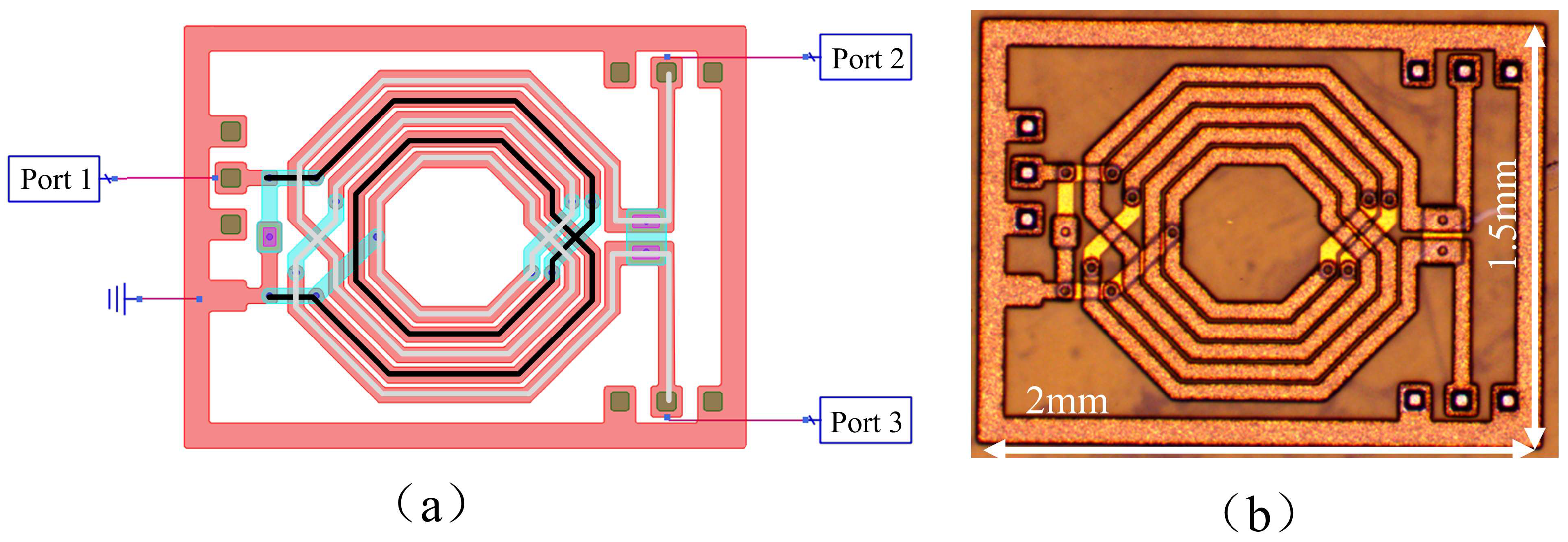
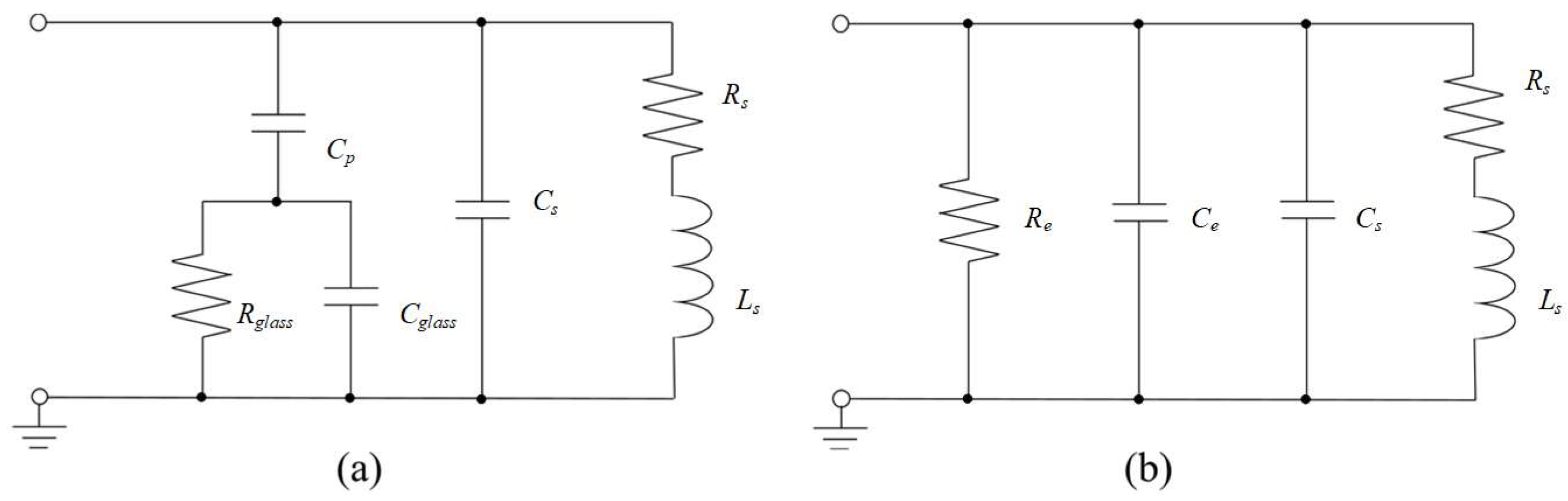
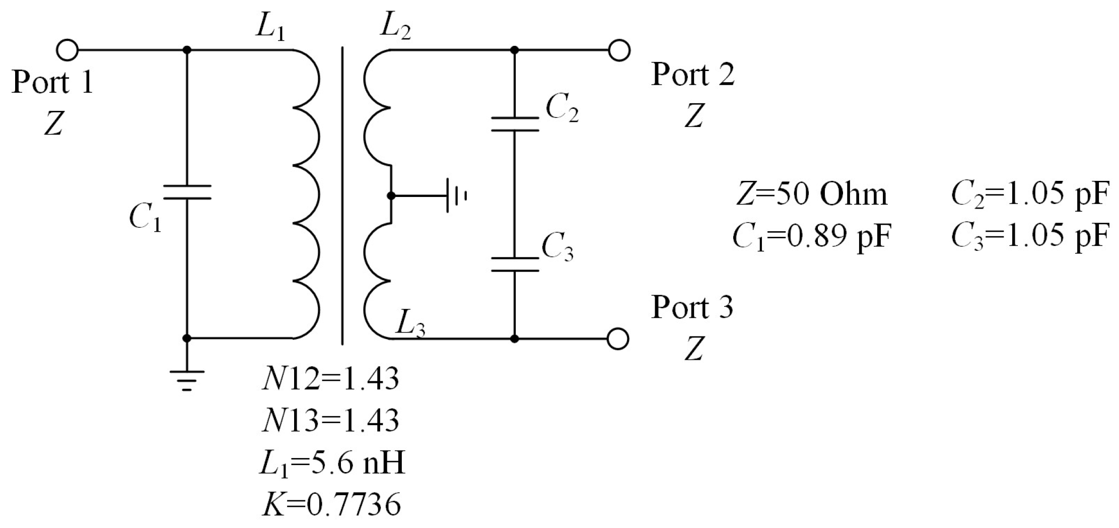
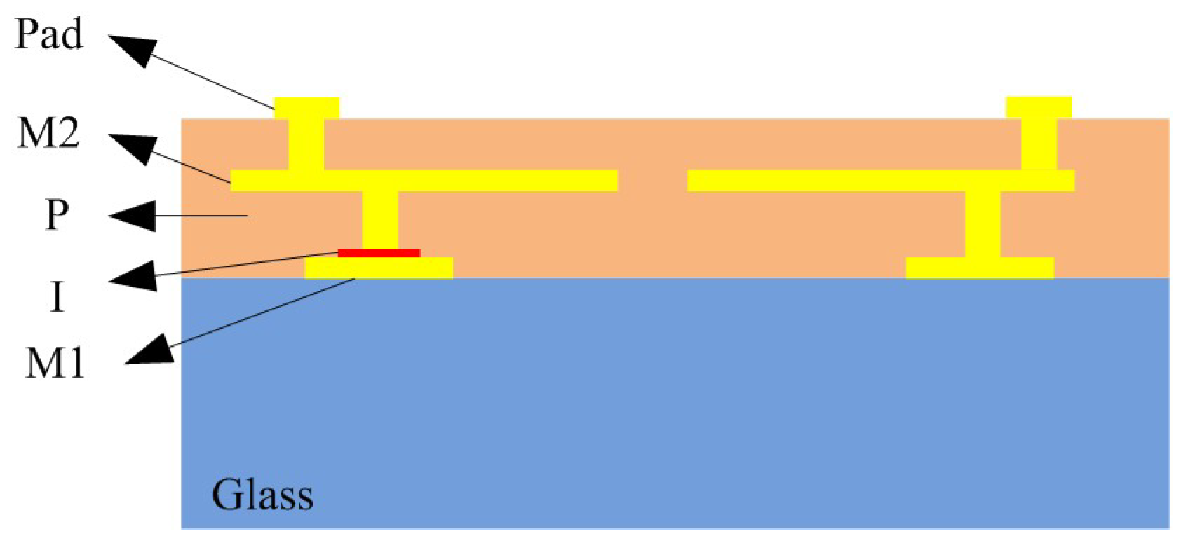
2. Design and Simulation
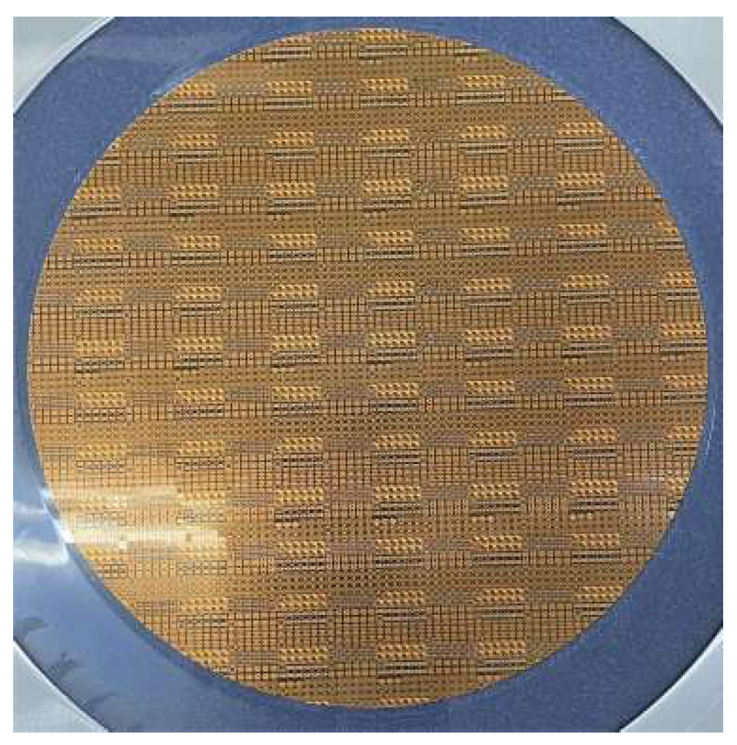
3. Processing
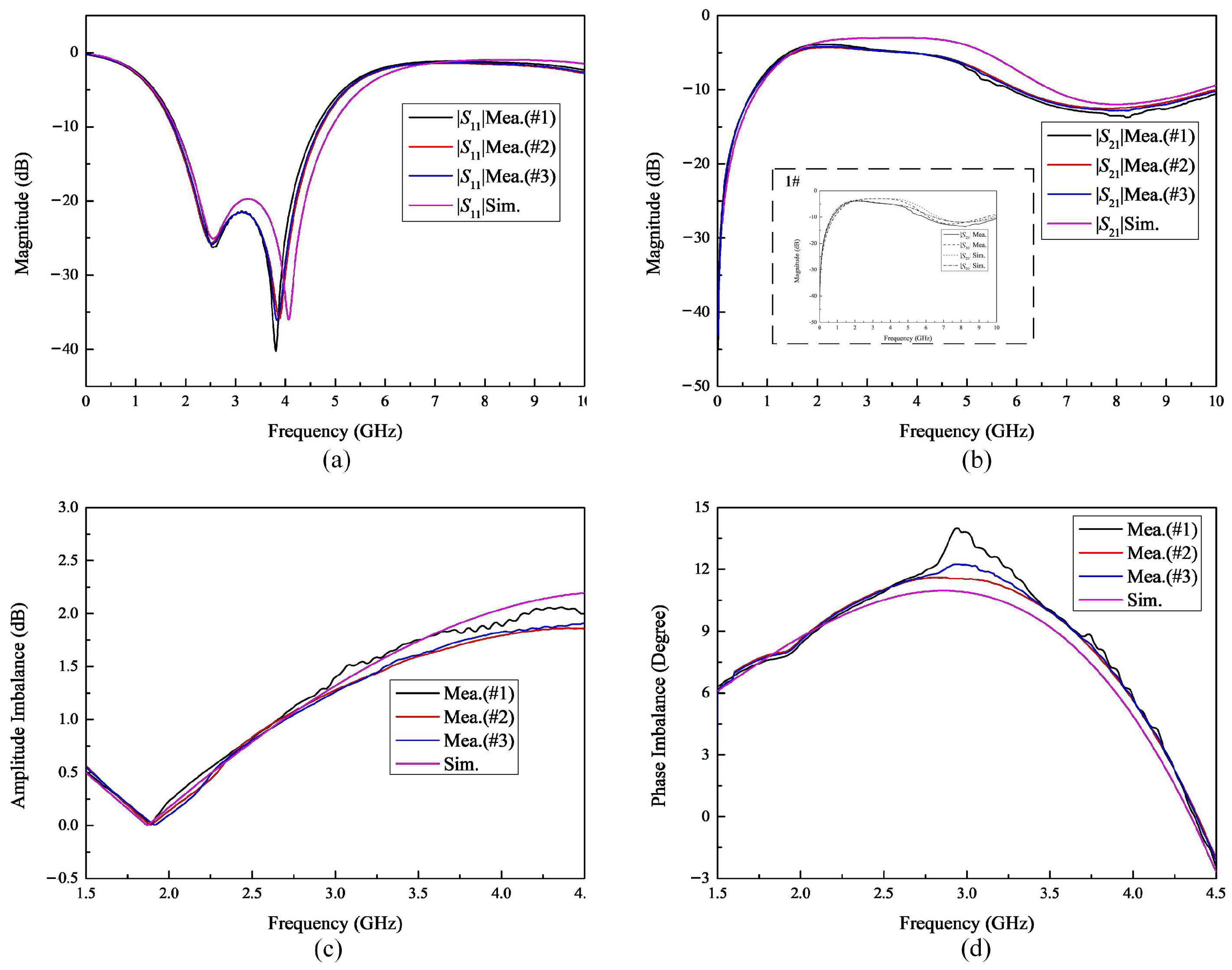
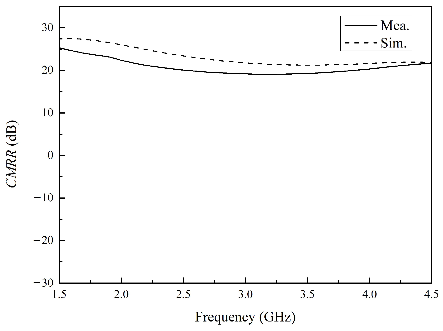
4. Results
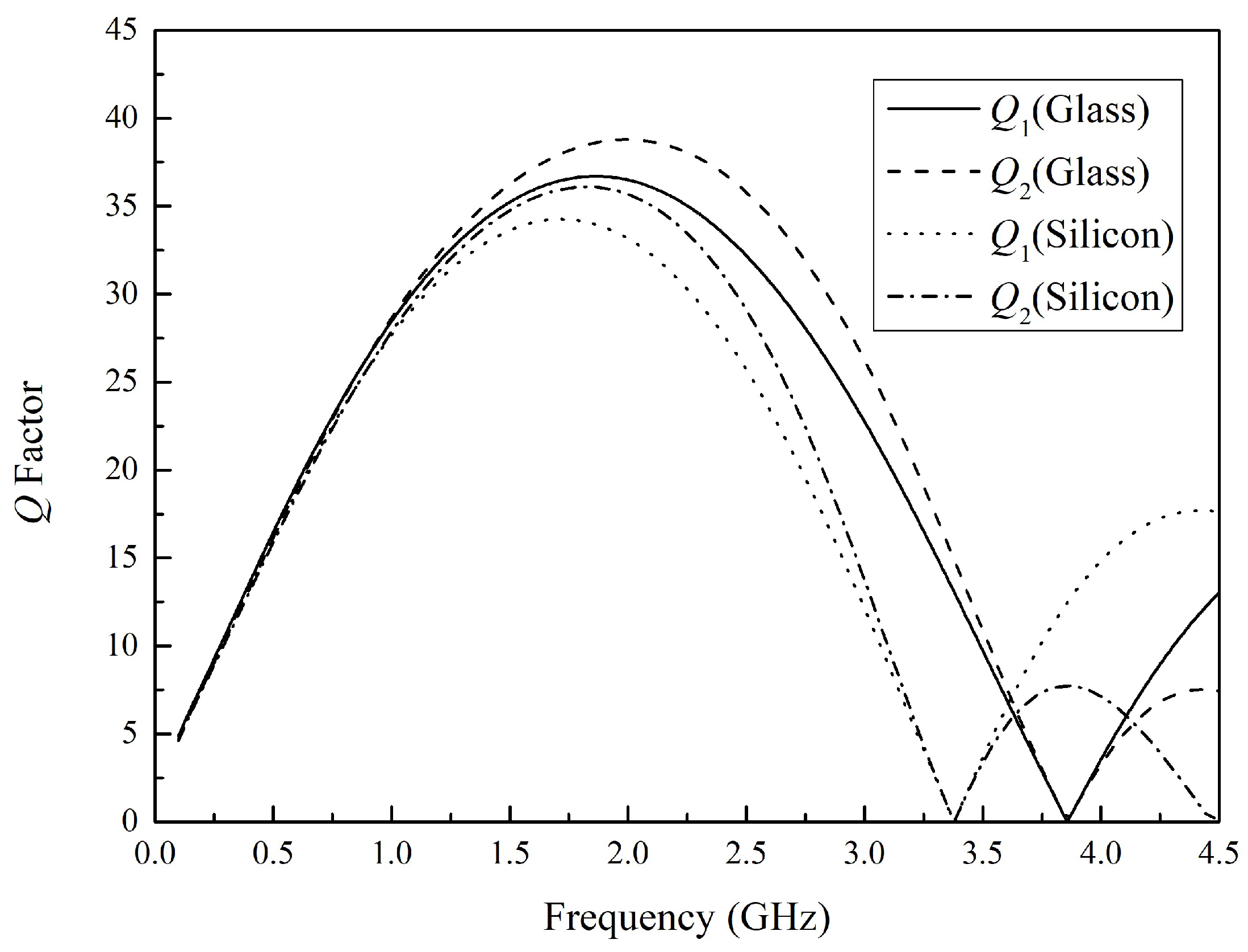
5. Discussion
6. Conclusions
Author Contributions
Funding
Data Availability Statement
Conflicts of Interest
References
- Zhang, L.; Dang, W.; Wang, Y.; Zhang, J. Ultrathin Small Outline Package Key Techniques for High-Speed Chips with Multi-Leads. Micromachines 2024, 15, 1029. [Google Scholar] [CrossRef] [PubMed]
- Tian, W.; Dang, H.; Li, D.; Cong, Y.; Chen, Y. Reliability Simulation Analysis of TSV Structure in Silicon Interposer under Temperature Cycling. Micromachines 2024, 15, 986. [Google Scholar] [CrossRef] [PubMed]
- Kim, C.; Senior, D.E.; Shorey, A.; Kim, H.J. Through-glass interposer integrated high quality RF components. In Proceedings of the 64th Electronic Components and Technology Conference (ECTC), Lake Buena Vista, FL, USA, 27–30 May 2014. [Google Scholar] [CrossRef]
- Demirhan Aydin, G.; Akar, O.S.; Akin, T. Wafer Level Vacuum Packaging of MEMS-Based Uncooled Infrared Sensors. Micromachines 2024, 15, 935. [Google Scholar] [CrossRef] [PubMed]
- Usman, A.; Shah, E.; Satishprasad, N.B.; Chen, J.; Bohlemann, S.A.; Shami, S.H.; Eftekhar, A.A.; Adibi, A. Interposer Technologies for High-Performance Applications. IEEE Trans. Compon. 2017, 7, 819–828. [Google Scholar] [CrossRef]
- Vivek, S.; Madhavan, S.; Tapobrata, B. Enhancing Signal and Power Integrity Using Double Sided Silicon Interposer. IEEE Microw. Wirel. Compon. Lett. 2011, 21, 598–600. [Google Scholar] [CrossRef]
- Gao, M.-J.; Ma, Y.-C.; Halimu, Y.; Liang, J.-G.; Jiang, Y.-F.; Qiang, T. A Low-Loss and High Phase Matching Balun Chip Based on Integrated Passive Technology for S-band RF System. In Proceedings of the 2022 10th International Symposium on Next-Generation Electronics (ISNE), Wuxi, China, 5–12 May 2023. [Google Scholar] [CrossRef]
- Ren, X.; Wei, J.; Yu, D. Design and Fabrication of High Density 3D IPDs (Integrated Passive Devices) on Glass Substrate. In Proceedings of the 2020 IEEE International Conference on Integrated Circuits, Technologies and Applications (ICTA), Nanjing, China, 23–25 November 2020. [Google Scholar] [CrossRef]
- Cai, C.; Wang, J.; Zhu, L.; Wu, W. A New Approach to Design Microstrip Wideband Balun Bandpass Filter. IEEE Microw. Wirel. Compon. Lett. 2016, 26, 116–118. [Google Scholar] [CrossRef]
- Guo, Y.; Wang, Q.; Chen, J. S-band Band-pass Filter by Using Integrated Passive Device Technology. In Proceedings of the 2022 23rd International Conference on Electronic Packaging Technology (ICEPT), Dalian, China, 10–13 August 2022. [Google Scholar] [CrossRef]
- Xu, M.; Lin, Z.; Su, J. Design and Simulation of Triple-Band Directionl Coupler Based on Integrated Passive Devices Process. In Proceedings of the 2023 IEEE MTT-S International Wireless Symposium (IWS), Qingdao, China, 16–19 May 2023. [Google Scholar] [CrossRef]
- Chen, W.; Wu, Y.; Wang, W. Wideband Bandpass Filtering Balun with Perfect In-Band Matching and Isolation. IEEE Trans. Circuits Syst. II Express Briefs 2020, 67, 1884–1888. [Google Scholar] [CrossRef]
- Kong, M.; Wu, Y.; Zhuang, Z.; Wang, W.; Wang, C. Ultraminiaturized Wideband Quasi-Chebyshev/-Elliptic Impedance-Transforming Power Divider Based on Integrated Passive Device Technology. IEEE Trans. Plasma Sci. 2020, 48, 858–886. [Google Scholar] [CrossRef]
- Khiabani, N.; Chiang, C.-W.; Liu, N.-C.; Kuan, Y.-C.; Wu, C.-T.M. An Ultrawide Ku-To-W Band Array Antenna Package Using Flip-Chipped Silicon Integrated Passive Device with Multilayer PCB Technology. IEEE Microw. Wirel. Compon. Lett. 2021, 31, 861–864. [Google Scholar] [CrossRef]
- Wang, C.; Kim, N.Y. High performance WLAN balun using integrated passive technology on SI-GaAs substrate. Microw. Opt. Technol. Lett. 2012, 1301–1305. [Google Scholar] [CrossRef]
- Chang, C.; Lin, Y. Balun bandpass filter with wide upper stopband using silicon-based integrated passive device technology. In Proceedings of the 2015 IEEE MTT-S International Microwave Workshop Series on Advanced Materials and Processes for RF and THz Applications (IMWS-AMP), Suzhou, China, 1–3 July 2015. [Google Scholar] [CrossRef]
- Yue, C.P.; Wong, S.S. On-chip spiral inductors with patterned ground shields for Si-based RF ICs. IEEE J. Solid-State Circuits 1998, 33, 743–752. [Google Scholar] [CrossRef]
- Amalu, N.I.; Okorie, B.A.; Ugwuoke, J.C.; Obayi, C.S. Electrical Conductivity of Spark Plasma Sintered W-Cu and Mo-Cu Composites for Electrical Contact Applications. J. Miner. Mater. Charact. Eng. 2021, 9, 48–60. [Google Scholar] [CrossRef]
- Greenhouse, H.M. Design of planar rectangular microelectronic inductors. IEEE Trans. Parts Hybrids Packag. 1974, PHP-10, 101–109. [Google Scholar] [CrossRef]
- Frye, R.C.; Hlaing, P.; Liu, K. High CMRR in reduced-coupling monolithic baluns. In Proceedings of the 2010 IEEE MTT-S International Microwave Symposium, Anaheim, CA, USA, 23–28 May 2010. [Google Scholar] [CrossRef]
- Geng, Y.F.; Wang, W.W.; Chen, X.W. The study and design of a miniaturized microstrip balun with a wider bandwidth. IEEE Antenna Wirel. Propag. Lett. 2016, 15, 1727–1730. [Google Scholar] [CrossRef]
- Mahdi, M.; Tork, H.; Darwish, M.; El-Tager, A.M. S-Band Single-Layer Balun for Wideband Applications. In Proceedings of the 2023 International Telecommunications Conference (ITC-Egypt), Alexandria, Egypt, 18–20 July 2023. [Google Scholar] [CrossRef]
- Glubokov, O.A.; Shelkovnikov, B.N. Broadband Balun in LTCC Technology Using Vertical Solenoid Coupled Transmission Lines. In Proceedings of the TELSIKS 2005—2005 Youth International Conference on Telecommunication in Modern Satellite, Cable and Broadcasting Services, Nis, Serbia, 16–19 October 2005. [Google Scholar] [CrossRef]
- Lew, D.-W.; Park, J.-S.; Ahn, D.; Kang, N.-K.; Yoo, C.; Lim, J.-B. A design of the ceramic chip balun using the multilayer configuration. IEEE Trans. Microw. Theory Tech. 2001, 49, 220–224. [Google Scholar] [CrossRef]
- Ma, Q.; Tie, H.; Zhou, B. Compact LTCC Balun using L-C Embraced Structure for 128 MHz 3T MRI Applications. Radioengineering 2022, 4, 455–459. [Google Scholar] [CrossRef]


| Layer | Material | Thickness (μm) | Relative Permittivity | Dielectric Loss Tangent | Conductivity (S/m) [18] |
|---|---|---|---|---|---|
| Pad | Cu | 8 | / | / | 5.80 × 10⁷ |
| M2 | Cu | 5 | / | / | 5.80 × 10⁷ |
| P | Polymide | 20 | 3.16 (5 GHz) | 0.0109 (5 GHz) | 0 |
| I | SiNx | 0.2 | 6.8 (5 GHz) | 0.0025 (5 GHz) | 0 |
| M1 | Cu | 5 | / | / | 5.80 × 10⁷ |
| Glass | Glass | 250 | 4.4 (5 GHz) | 0.0057 (5 GHz) | 0 |
| Technology | Bandwidth/GHz | Insertion Loss/dB | Amplitude Imbalance/dB | Phase Imbalance/(°) | Size (mm × mm) | CMRR /dB | |
|---|---|---|---|---|---|---|---|
| [21] | PCB | 1.19–3.25 | <5.1 | <0.49 | <6.5 | 18 × 17.5 | / |
| [22] | PCB | 2–4 (>11 dB) | <0.75 | <0.6 | <7 | 0.85λg2 | >15 |
| [23] | LTCC | 0.8–3 | <6 | <0.7 | <6 | 3.05 × 1.3 | / |
| [24] | Multilayer configuration | 0.5–1.3 | 1.0 | / | 180 ± 3% | 3.2 × 1.6 | / |
| [25] | LTCC | 0.11–0.14 | 3.3 | 0.18 | <1 | 8.5 × 9.5 | / |
| This work | IPD | 2.07–4.30 | <2.50 | <2 | <14.02 | 1.81 × 1.36 | >19.08 |
Disclaimer/Publisher’s Note: The statements, opinions and data contained in all publications are solely those of the individual author(s) and contributor(s) and not of MDPI and/or the editor(s). MDPI and/or the editor(s) disclaim responsibility for any injury to people or property resulting from any ideas, methods, instructions or products referred to in the content. |
© 2025 by the authors. Licensee MDPI, Basel, Switzerland. This article is an open access article distributed under the terms and conditions of the Creative Commons Attribution (CC BY) license (https://creativecommons.org/licenses/by/4.0/).
Share and Cite
Qian, J.; Wu, P.; Quan, H.; Wang, W.; Wang, Y.; Sun, S.; Xia, J. An On-Chip Balun Using Planar Spiral Inductors Based on Glass Wafer-Level IPD Technology. Micromachines 2025, 16, 443. https://doi.org/10.3390/mi16040443
Qian J, Wu P, Quan H, Wang W, Wang Y, Sun S, Xia J. An On-Chip Balun Using Planar Spiral Inductors Based on Glass Wafer-Level IPD Technology. Micromachines. 2025; 16(4):443. https://doi.org/10.3390/mi16040443
Chicago/Turabian StyleQian, Jiang, Peng Wu, Haiyang Quan, Wei Wang, Yong Wang, Shanshan Sun, and Jingchao Xia. 2025. "An On-Chip Balun Using Planar Spiral Inductors Based on Glass Wafer-Level IPD Technology" Micromachines 16, no. 4: 443. https://doi.org/10.3390/mi16040443
APA StyleQian, J., Wu, P., Quan, H., Wang, W., Wang, Y., Sun, S., & Xia, J. (2025). An On-Chip Balun Using Planar Spiral Inductors Based on Glass Wafer-Level IPD Technology. Micromachines, 16(4), 443. https://doi.org/10.3390/mi16040443