Review

Tunnel Junction with Perpendicular Magnetic Anisotropy: Status and Challenges

1
Spintronics Interdisciplinary Centre & School of Electronic and Information Engineering, Beihang University, Beijing 10191, China
2
Institute of Fundamental Electronics (IEF), University of Paris-Sud, Orsay 91405, France
*
Author to whom correspondence should be addressed.
Micromachines 2015, 6(8), 1023-1045; https://doi.org/10.3390/mi6081023
Submission received: 29 June 2015 / Revised: 29 June 2015 / Accepted: 4 August 2015 / Published: 10 August 2015

Abstract

:
Magnetic tunnel junction (MTJ), which arises from emerging spintronics, has the potential to become the basic component of novel memory, logic circuits, and other applications. Particularly since the first demonstration of current induced magnetization switching in MTJ, spin transfer torque magnetic random access memory (STT-MRAM) has sparked a huge interest thanks to its non-volatility, fast access speed, and infinite endurance. However, along with the advanced nodes scaling, MTJ with in-plane magnetic anisotropy suffers from modest thermal stability, high power consumption, and manufactural challenges. To address these concerns, focus of research has converted to the preferable perpendicular magnetic anisotropy (PMA) based MTJ, whereas a number of conditions still have to be met before its practical application. This paper overviews the principles of PMA and STT, where relevant issues are preliminarily discussed. Centering on the interfacial PMA in CoFeB/MgO system, we present the fundamentals and latest progress in the engineering, material, and structural points of view. The last part illustrates potential investigations and applications with regard to MTJ with interfacial PMA.

1. Introduction

Following Moore’s law, the development of semiconductor industry, especially the complementary metal oxide semiconductor (CMOS) technology, has deeply impacted the world since 1970s. However, as the advanced node scaling goes below 45 nm, static power consumption increases faster than the dynamic power consumption due to intrinsic current leakage, which challenges the progress of very large scale integrated circuits (VLSI). Additionally, the long distance data traffic between memory and logic chip causes large dynamic power consumption and interconnection delay [1]. In 2015, Gordon Moore claimed that his law would reach saturation during the next decade. Novel approaches based on spintronics has opened another avenue to continuous scaling, among which magnetic tunnel junction (MTJ) has been recommended as a potential replacement since its first proposal and demonstration [1,2,3].
MTJ is basically configured with ultra-thin multilayer, i.e., the free and reference layer comprising ferromagnetic metal with a sandwiched metal oxide film as tunnel barrier. Driven by external magnetic field or charge current, the magnetization direction of free layer can switch between parallel and antiparallel states (P and AP) relative to that of reference layer, thus the corresponding low or high resistance states (RL and RH) can be used for data storage. The margin of two resistance states is defined as tunnel magnetoresistance ratio (TMR ratio):
T M R   r a t i o = R H R L R L
Such characteristics allow the proposal and commercialization of magnetic random access memory (MRAM) by integrating the device onto the silicon based CMOS circuit, which demonstrates non-volatility, fast access speed, and infinite endurance. However, MTJ with amorphous Al2O3 tunnel barrier suffers from the modest TMR ratio below 70% [4], thus the reliability of reading operation cannot be assured. In 2004, high TMR ratio of 180% was observed by Yuasa et al. [5,6] from MTJ using single crystal MgO tunnel barrier as particular symmetry filter. Since then, MgO has become the mainstream material for tunnel barriers.
Moreover, the property of MTJ also relies on its magnetic anisotropy, specifically when current induced magnetization direction switching, i.e., the spin transfer torque (STT) switching, is taken into consideration. Tremendous work has been undertaken towards MTJ with in-plane magnetic anisotropy referring to shape anisotropy. Although having achieved giant TMR ratios up to 604% [7], in-plane magnetic anisotropy based MTJ still faces the obstacles from thermal stability and power consumption. Thermal stability is determined by energy barrier E between P and AP magnetization alignments:
E = M s H k V 2
where Ms is the saturation magnetization, Hk the anisotropy field, and V the volume of free layer. It is reasonable that scaled node weakens the shape anisotropy from the ellipse nano-pillar cross section, which is also difficult to fabricate when shrinking down to 22 nm. On the other hand, the out-of-plane precession during spin transfer torque (STT) switching contributes to the power consumption. These disadvantages can be eliminated by introducing perpendicular magnetic anisotropy (PMA), thus MTJ with PMA is promising to enable high-density low-power VLSI. Consequently, the key point of research turns to how to achieve strong PMA for practical application [8,9].
In the rest of this review, we firstly introduce the fundamentals of PMA and STT in the memory point of view, followed with the relevant description of fabrication and characterization methods. Considering the progress of PMA, especially interfacial PMA, we discuss the crucial challenges and potential solutions with respect to material, structure, and processing, as well as other attractive research and applications. Finally, we give a brief conclusion and prospective.

2. Perpendicular Magnetic Anisotropy Principles

PMA in periodic Co/Pd multilayer with Co layer thinner than 0.8 nm was observed by Carcia et al. [10] in 1985. They attributed its origin to the anisotropy at Co/Pd interface and the strain in Co thin film. For the multilayer based on transition and noble metal such as Co/Pd (Pt), PMA, saturation magnetization, anisotropy field, and other parameters can be easily modulated by adjusting the number of bilayer periods, as well as the thickness of each layer [10,11,12]. However, the face-centered cubic fcc Co/Pd (Pt) (111) multilayers possess low spin polarization compared to CoFeB or CoFe, and cannot favor the formation of MgO (001) tunnel barriers, thereby impeding the improvement of TMR ratio [13,14]; Moreover, the free layer thickness should be reduced for lower threshold current to manipulate magnetization direction reversal. Thus, Yakushiji et al. [15,16] developed the ultra-thin Co/Pd (Pt) multilayers configured with 0.14–0.2 nm films, which present not only large PMA, but also a relatively high TMR ratio of 62% and an ultra-low resistance area product (RA) with adherent CoFeB film. For the MTJ consists of CoFe/Pd multilayer, MgO tunnel barrier, and CoFeB insertion between, TMR ratio has been promoted to 78% after being annealed at 200 °C [17]. Even though, this kind of MTJ still suffers from complicated structure, weak thermal stability, and large damping constant α.
To realize general application, especially the low-power spin transfer torque magnetic random access memory (STT-MRAM), numerous materials and structures have been studied, among which amorphous rare earth transition metal alloys (e.g., TbCoFe) attract interest due to their large PMA and remnant squareness. However, the employment of TbCoFe degrades the thermal endurance of MTJ, while the TMR ratio cannot be increased by post-deposition annealing because no MgO crystallization happens [18].
The milestone of PMA is the CoFeB/MgO structure based MTJ proposed by Ikeda et al. [19] in 2010. This work reported excellent TMR ratio of 120%, high thermal stability, and low switching current of 49 μA at 40 nm diameter, hereafter the research focus has converted to the CoFeB/MgO interface. In detail, the easy axis turns from in-plane to out-of-plane direction when the thickness of CoFeB is reduced below 1.5 nm and exhibits a 3.4 kOe anisotropy field with 1.3 nm CoFeB film. With respect to the crystal structure, the amorphous CoFeB crystalized into body-centered cubic bcc (001) texture via MgO (001) template during post-deposition annealing. Therefore, in addition to the thickness variation of MgO tunnel barrier, lattice mismatch at CoFeB/MgO interface happens during the sputtering and annealing process, resulting in failure and reliability challenges of STT-MRAM [20]. Actually, first-principles calculation has predicted the existence of interfacial PMA in Fe/MgO bilayer prior to the experimental discovery [21]. Afterwards, Yang et al. [22] extended the study to Co/MgO interface. The origin of interfacial PMA is attributed to the overlap between Fe-3d and O-2p orbitals at the interface, as well as the spin-orbit coupling (SOC) induced Fe d orbitals hybridizations in out-of-plane direction.

3. Spin Transfer Torque: Fundamental and Memory Operation

STT effect was theoretically predicted by Slonczewski et al. [23,24] in 1996 and experimentally observed in MTJ with CoFe/Al2O3/CoFe structure in 2004. A charge current, instead of the external magnetic field for classic MRAM, is used to switch the free layer magnetization direction. The primary mechanism of STT switching can be illustrated with the typical one transistor one MTJ STT-MRAM cell shown in Figure 1a, where the write operation is performed by changing the polarity of charge current passing through the MTJ selected by bit and word line. The writing current can be spin polarized by the reference layer, transfer its spin angular momentum to free layer magnetic moment, and eventually reorient it by induced torque.
Figure 1. (a) One transistor one magnetic tunnel junction (MTJ) cell using mechanism of spin transfer switching, where the MTJ is selected by word line and transistor, and operated by bit line. (b) Comparison between in-plane and perpendicular anisotropy based MTJ nano-pillar [25].
Micromachines 06 01023 g001
After the significant enhancement of TMR ratio realized by replacing Al2O3 with MgO tunnel barrier, the first STT switching of perpendicular magnetic moment was clearly observed in MTJ with TbCoFe/CoFeB/MgO/CoFeB/TbCoFe structure fabricated at room temperature [26]. Although low threshold current density of 4.7 × 10⁶ A/cm2 has been achieved in comparison with in-plane magnetic anisotropy based MTJ, the TMR ratio is only 15% for the reason mentioned before. The theoretical expression of threshold current is:
I c 0 = α γ e μ B g M s H k V
where the notation α is the damping constant, γ the gyromagnetic constant, e is the charge of electron, μB is the Bohr Magnetron, and g is a parameter determined by the spin polarization and the angle between free and reference layer magnetization directions. Another parameter should be concerned with is thermal stability factor, which is defined as:
Δ = E k B T = K e f f V k B T
where E denotes energy barrier as Equation (2), Keff the effective anisotropy energy constant defined by Keff = E/V, kB the Boltzmann constant, and T the absolute temperature. It is evident that both Ic0 and Δ are in direct proportion to device dimension, which means Keff should be elevated with technology node shrinking to ensure 10 year data retention against thermal fluctuation. For instance, the design of gigabit memory with 1X nm PMA MTJ requires Keff larger than 107 erg/cm3 for Δ more than 40. Furthermore, the compromise between low power consumption and long retention time can be reached through α reduction, thus the ratio of Δ/Ic0 considered without the influence introduced by Δ variation among devices.
Compared with in-plane magnetic anisotropy based MTJ, whose energy barrier E originates from the asymmetric ellipse shape, PMA based MTJ depends on the interfacial atom arrangement, thus circular device which is more manufacturable can be adopted for smaller feature size (Figure 1b). On the other hand, Ic0 of MTJ with PMA is lower for the cancel of demagnetization field. In view of this, PMA based MTJ has been recommended as the most potential candidate to realize high-density memory. Additionally, the write and read speed of PMA based MTJ should be minimized to further enable the replacement of static random access memory (SRAM) and embedded dynamic RAM (eDRAM) [9]. Although switching speed of 1 ns using writing current as eight times as Ic0 has been reported by Worledge et al. [27] in 2011, the fastest data obtained from in-plane magnetic anisotropy based MTJ is 190 ps [28]. It is worth noting that the switching speed is determined by the amplitude of writing current rather than the orientation of magnetic moment, because the switching mode transits from being processional to thermal fluctuation assisted by STT along with extended pulse duration, further indicating the importance to pursue lower Ic0.

4. Fabrications and Measurements of STT-MRAM Device

The integration of STT-MRAM is an “above IC” process, thus the adjustment of MTJ device process to standard CMOS technology is absolutely required to realize potential applications (Figure 2a). Generally speaking, the fabrication mainly comprises substrate preparation, stack deposition, annealing, etching, dielectric encapsulation, and wiring; each procedure should be carefully examined with relevant equipment and instruments. Figure 2b depicts the typical flow of art.
Figure 2. (a) Topology of spin transfer torque magnetic random access memory (STT-MRAM) with two cells atop the silicon based complementary metal oxide semiconductor (CMOS) front-end circuit. M1/M2 and V1 denote different level of metal layers and via, separately. (b) Typical flow of MTJ device fabrication corresponding to (a).
Micromachines 06 01023 g002

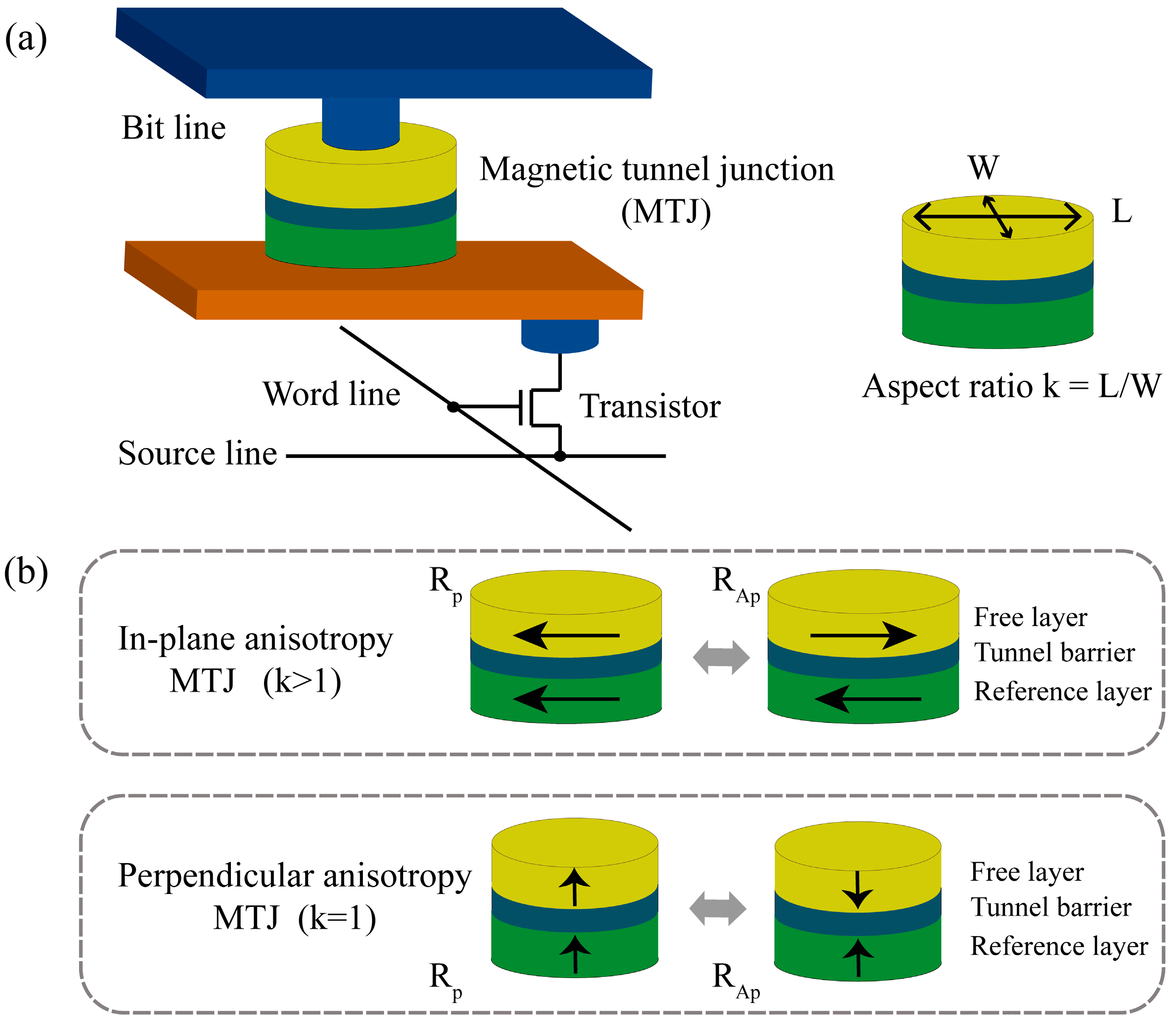
4.1. Magnetic Tunnel Junction Device Process Technology

4.1.1. Substrate Preparation

To produce STT-MRAM chip, the transistor-based circuit can be prepared in front end of line (FEOL) process by standard COMS technology. Then, an insulation layer (e.g., SiN) is deposited on the substrate, where metal contacts are formed for the interconnection between CMOS circuit and MTJ stack. Surface roughness is a critical parameter requiring optimization to avoid Neel coupling, hence the procedure usually ends up with polish by chemical mechanical planarization (CMP) or other methods. Moreover, film defects, oxidation, and CMP residual should be minimized against open/short circuit or other negative situations. For the experimental fabrication, thermally oxidized Si wafer is preferred as substrate for the favorable properties and prices. Pre-cleaning is necessary to ensure device quality and measurement accuracy, e.g., ultra-sound bathed in acetone for one hour, followed by nitrogen drying and optical microscope check.

4.1.2. Stack Deposition

Following the preparation of smooth substrate, ultra-thin films of MTJ stack can be grown with advanced deposition tools, among which the typical ones includes sputtering or molecular beam epitaxy (MBE) systems. The base pressure in the ultra-high vacuum chamber should be lower than 10−8 Torr to obtain optimum interfacial PMA. Deposition rate should be controlled under 0.1 nm/s to accurately regulate the thickness of ultra-thin film, as well as the uniformity and oriented texture. Firstly, at least one nonmagnetic metal buffer layer is deposited to benefit surface flatness, film adhesion, and crystalline growth (e.g., Ta/Ru/Ta). Then, the essential part of MTJ stack (e.g., CoFeB/MgO/CoFeB) can be grown; in the case of in-plane magnetic anisotropy based MTJ, pinned layer of antiferromagnetic metal (e.g., PtMn) should be deposited adjacent to reference layer to fix the magnetization direction. Finally, at least one nonmagnetic capping layer (e.g., Ta/Ru/Ta/Ru) should be coated for protection, as well as for interfacial PMA induction in certain configuration.
How to grow perfect MgO (001) tunnel barrier is the most notable challenge of this procedure. Giant TMR ratio has been achieved using MBE [5]. With sputtering, this film is usually deposited from MgO target by radio-frequency magnetron gun under Ar atmosphere. Pre-sputtering Ta getter has been suggested as one of the effective method to remove H2O and O2 residual gas before MgO deposition, which improves the stoichiometry and interstitial defects in tunnel barriers. Another method is to deposit Mg metal first and then strictly oxidize it into MgO by either natural or plasma process [29]. High quality of MgO tunnel barriers enables the achievement of giant TMR ratio and acceptable RA. However, the thickness variation and lattice mismatch issues noted before still need to be solved for high reliability.
In view of throughput and quality, sputtering should be the most suitable tool to realize mass manufacture and general application, thus Canon ANELVA (Kawasaki, Japan), SINGULUS TECHNOLOGIES (Kahl am Main, Germany), and other tool vendors, have developed advanced systems capable of processing 300 mm diameter wafers with multiple sources in one chamber. Take the tool of IBM for illustration, this system is an integration of sputtering, oxidation, and pre-cleaning chambers, where wafers can be transferred with a central robot without breaking the vacuum. Nevertheless, there is still space for promotion.

4.1.3. Post-Deposition Annealing

After MTJ stack deposition, the sample is subsequently annealed at ~300 °C in vacuum for certain time, e.g., 1 h. Effect of this heat treatment can be illuminated from structural and natural points of view. As has been mentioned, with (001) texture MgO as template, the amorphous CoFeB can crystalized into bcc (001) texture at high temperature, which is critical to generate high TMR ratio, as well as interfacial PMA in CoFeB/MgO structure based MTJ. Moreover, the annealing temperature dependent tendency of magnetization M and Keff can be observed in Figure 3 [30], where the initial increase can be attributed to the B absorption by Ta, and the later decrease arises from the formation of additional magnetic dead layer. Referring to in-plane magnetic anisotropy based MTJ, this procedure should be performed in an external magnetic field around 10 kOe to fix the magnetization direction reference layer through the exchange bias with pinned layer. However, the standard CMOS fabrication temperature is 400 °C, hence the integration of MTJ device demands robust compatibility with elevated temperature. This is a key challenge for the commercial development of MRAM or STT-MRAM.
Figure 3. Annealing temperature dependence of (a) magnetic moment per unit volume (m/V); (b) Keff for films Ta 1/CoFeB t/MgO 2/Ta 1 (units in nm): t is 0.6 nm for the black squares and 1.2 nm for the red circle. Reproduced with permission from Sinha et al. [30], Journal of Applied Physics; published by AIP Publishing, 2015.
Micromachines 06 01023 g003

4.1.4. Device Etching

After magnetic measurement certification, the blanket MTJ stack is patterned into a nanoscale device with lithography and etching process. Ultra-violet lithography (UVL) can define photomask of micron order, while the delicate MTJ shape needs to use electron beam lithography (EBL) for ultra-high resolution. Available etchers have evolved from ion beam etching (IBE) to diverse options, including reactive ion etching (RIE), inductively coupled plasma (ICP), and other systems, from which more than one technique are often chosen and mixed.
First, the bottom electrode is patterned with hard mask to bridge the metal contact below and MTJ on the top. Typical hard mask materials include SiO2, Ta, and TiN, and the pattern is transferred from photoresist photomask by ICP/RIE. The difficulty of patterning is significantly reduced due to the circular shape of PMA based MTJ device.
Second, hard mask for MTJ device etching is defined by EBL and ICP/RIE following a similar route, with which unnecessary material is subsequently removed by IBE or other methods for nano-pillar profile. The nanoscale etching usually terminates over MgO tunnel barrier or penetrates it, leaving certain conductive films as the bottom electrode. This can be accurately monitored by secondary ion mass spectroscopy (SIMS) end point detector mounted in the process chamber. During the process, shorts across MgO tunnel barrier, which is a limit for yield, may be caused by non-volatile residuals redeposited on sidewall.
Here, it is meaningful to highlight the art of IBE/RIE/ICP. IBE has been a general apparatus for MTJ device fabrication in both laboratory and industry (Figure 4a). This technique is fully based on physical mechanism, i.e., removing surface atoms with the force of incident ion beam. IBE can be universally used for most materials with little chemical damage to magnetic property, whereas the device obtained suffers redeposition and shadow effect. Wafer tilt and rotation can improve the device profile, but limits its application in high-density array patterning [31]. Besides, enlarging the size of ion source to deal with 300 mm wafer while maintaining beam uniformity and directionality remains a challenge [32,33]. In contrast, RIE/ICP are more suited for mass production. Introduced by RIE, chemical reaction provides the possibility of material dependent etching selectivity, which quite contributes to endpoint detection as well as morphology control. However, Cl based RIE requires processing temperature over 350 °C to enable product volatilization, which detrimentally impacts the magnetic property [34,35]. Other plasmas, e.g., NH3/CO [36] and Methanol [37], also more or less present pros and cons. ICP presented in Figure 4b is another type of RIE. High-density plasma can be generated from electromagnetic induction, thus bringing enhanced anisotropy.
Third, compared with in-plane magnetic anisotropy based MTJ, the negative influence from etching on PMA based MTJ is more sensitive because smaller size is considered. Practically, MTJ device property degradation (e.g., coercivity and TMR ratio decrease) induced by either method is the major issue to be overcome. Kinoshita et al. [38] investigated this damage and proposed post-etching treatment using reductive He/H2 plasma, specifically for the CoFeB/MgO structure based MTJ with interfacial PMA. In this study, Methanol gas, which exhibits high etching selectivity against Ta hard mask, was used to conduct ICP processing. After He/H2 plasma treatment at 180 °C for 150 s, TMR ratio almost restored to the IBE level, and this trend can only be observed with pillar below 97 nm in size. Therefore, post-etching recovery is a necessary procedure for the scalability of PMA based MTJ.
Figure 4. Schematic illustration of (a) ion beam etching (IBE) with endpoint detector (EPD), i.e., secondary ion mass spectroscopy (SIMS), wafer tilt and rotation; (b) inductively coupled plasma (ICP) using an optical emission spectrometer (OES).
Micromachines 06 01023 g004

4.1.5. Dielectric Encapsulation

During the procedure, an insulation layer (e.g., SiO2) is deposited over the bottom electrode and MTJ nano-pillar by plasma enhanced chemical vapor deposition (PECVD) or other methods for electric protection. This procedure is preferred to be performed in-situ, because Mg(OH)2 forms instantly with MgO tunnel barrier in presence of water, leading to device property deterioration. Besides, standard temperature of PECVD for CMOS fabrication is 400 °C, where magnetic property of MTJ devices suffer. Accordingly, magnetic and dielectric material engineering should reach a compromise focusing on processing temperature. Without regard to output, a low-temperature technique for encapsulation is atom layer deposition (ALD), which demonstrates well controlled precision and isotropy.

4.1.6. Wiring

The final procedure is to create a connection between the MTJ device and peripheral circuit. Chemical mechanical polishing (CMP) can be undertaken at first to smooth the insulating layer surface, where contact is defined with photomask and opened until the underlying capping layer is exposed. Then, nonmagnetic metal (e.g., copper) can be deposited upon, followed with another CMP to remove the undesired wiring metal. This is the so called damascene process.

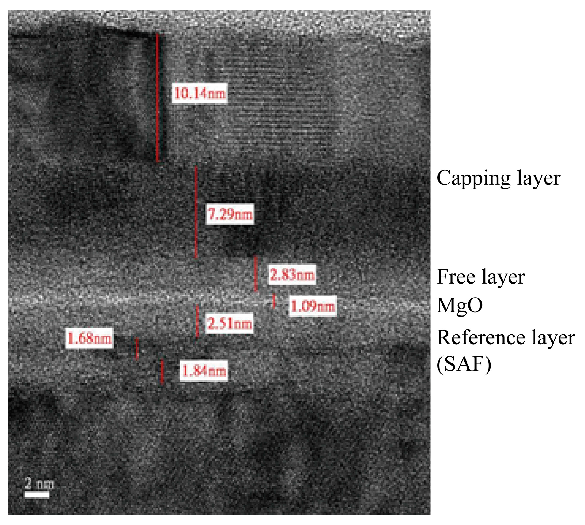
4.2. Property and Morphology Characterization

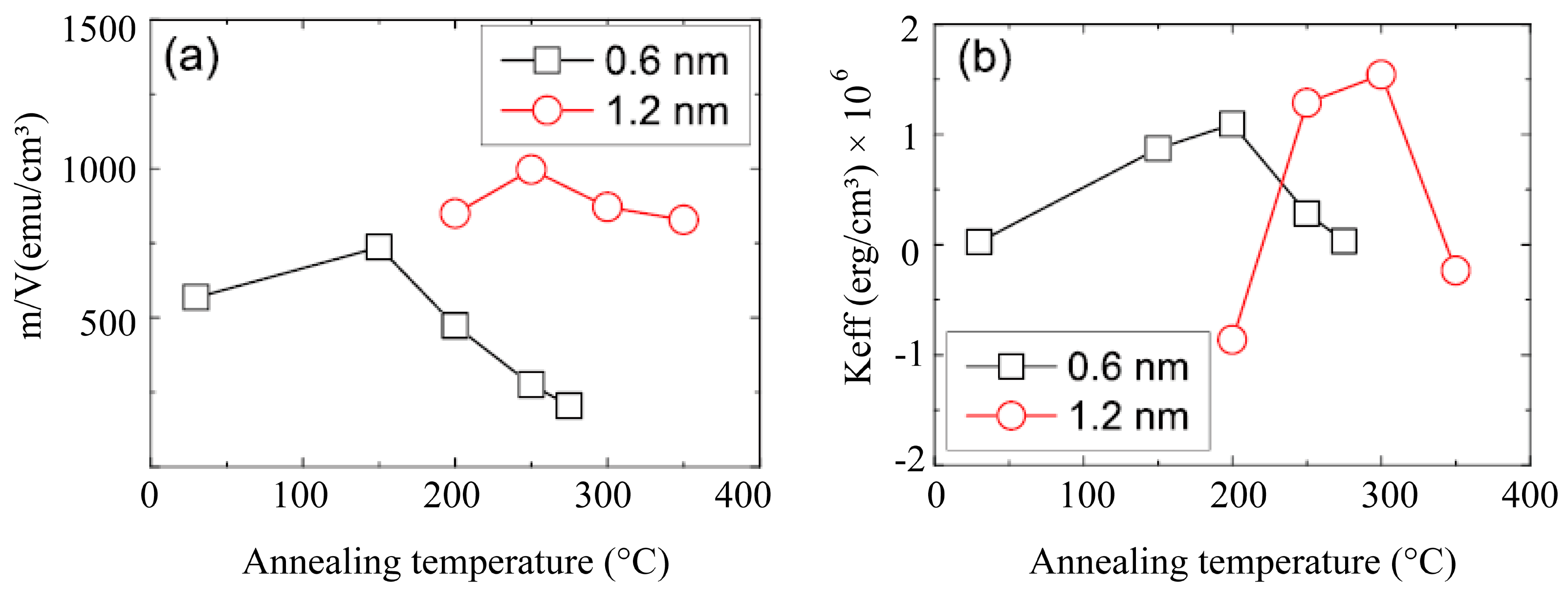
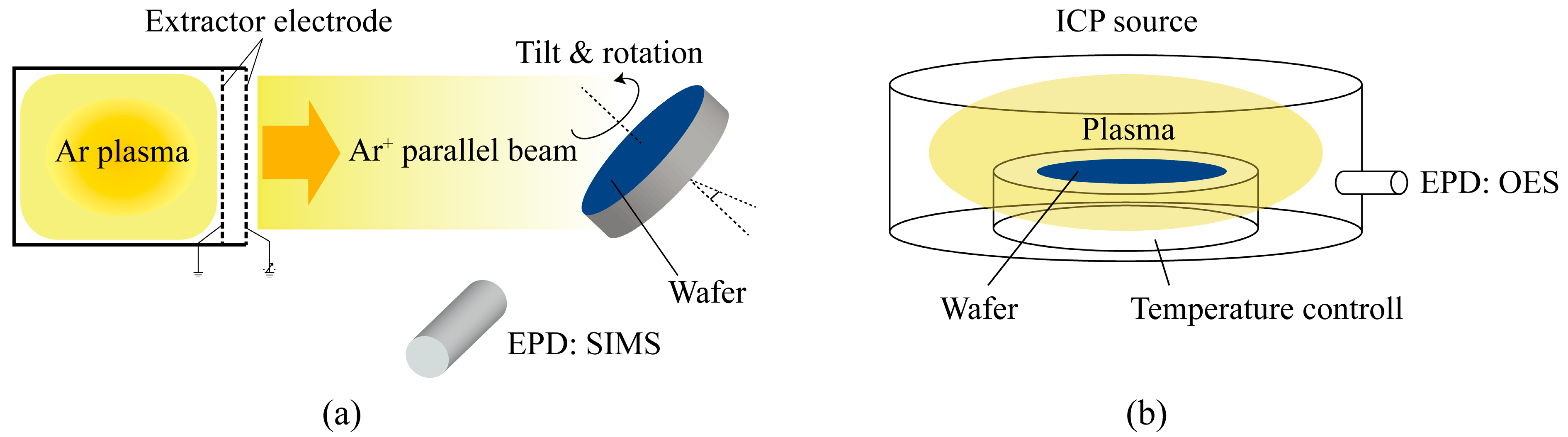
Magnetic Measuring Method

The vibrating-sample magnetometer (VSM) based on Faraday’s law is the most general metrology equipment to characterize blanket MTJ ultra-thin films at room temperature. For MTJ sample with PMA, magnetic moment versus external out-of-plane and in-plane magnetic field (m-H) curves reveal the existence of perpendicular easy axis. For the sample with interfacial PMA, saturation magnetization MS and magnetic dead layer thickness td can be given by linear fitting on m and CoFeB thickness t in the equation below:
m / A = M ( t t d )
where A denotes the area of MTJ nano-pillar. Furthermore, Keff is determined by bulk anisotropy constant Kb, demagnetization field 2πMS2, and interfacial anisotropy constant Ki, as the equation shown:
K eff = K b 2 π M S 2 + K i / t eff
here, teff is the effective CoFeB thickness determined with teff = ttd. Fitting results from Equation (6) have indicated the existence of PMA at CoFeB/MgO interface while that Kb is negligible.
Similar measurement techniques include superconducting quantum interference device (SQUID), magneto-optic Kerr effect (MOKE) magnetometer and other instruments. Each method performs differently on resolution, accuracy, sensitivity and other specifications, thus compromise should be reached according to the particular situation. Besides, TMR ratio can be quantified with current-in-plane tunneling (CIPT) method.
The film structure can be investigated by transmission electron microscope (TEM) with specially ion milled sample. As the cross-section image shown in Figure 5, free and synthetic antiferromagnetic (SAF) reference layers separated by ultra-thin 1.09 nm MgO tunnel barrier can be recognized with high resolution. During the nano-pillar etching procedure, scanning electron microscope (SEM) is an effective tool to examine device profile. In addition to critical dimension, how to achieve nearly-vertical sidewall angle (e.g., 80°) is another issue worth being concerned.
After the profile of MTJ nano-pillar is confirmed, the measurement can turn to its electrical performance, i.e., the STT behavior. Four-probe method is often used at room temperature for current induced magnetization direction switching, thus resistance curve can be evaluated as a function of applied current (R-I) in absence of external magnetic field. A series of intrinsic parameters can be characterized, such as threshold current, TMR ratio, and breakdown voltage. The yield detractor is usually the fort MTJ device due to etching redeposition mentioned before. Additionally, the quality of circuit integration should be assessed by testing certain amount of MTJ device for the process variation.
Figure 5. Cross-section image of MTJ stack, where free and synthetic antiferromagnetic (SAF) reference layers separated by ultra-thin 1.09 nm MgO tunnel barrier can be recognized respectively with high resolution.
Micromachines 06 01023 g005

5. Challenges and Enhancements towards Interfacial PMA

5.1. Material Engineering

5.1.1. CoFeB Behavior and Composition

The distribution of B in annealed MTJ multilayer is an interesting problem to clarify. Standing-wave (SW) hard x-ray photoemission spectroscopy (HXPS) analysis conducted by Greer et al. [39] using Co20Fe60B20 showed that 19.5% of B diffuses into MgO for Mg–B–O and 23.5% forms a thin TaB-like film at Ta/CoFeB interface, and certain theory related the achievement of high TMR ration with Mg–B–O. Meanwhile, other investigations controversially claimed that B migrates into Ta film if MgO barrier without O vacancy is fabricated [40]. On the basis of these published results, Mukherjee et al. [41] studied series of Ta/CoFeB/MgO samples and concluded that only by covering the top surface with Ta film can avoid the presence of B oxide at CoFeB/MgO interface.
On the other hand, it is not difficult to understand that the element ratio of CoFeB also has an effect on interfacial PMA. Ikeda et al. [42] published the experimental results towards PMA based MTJ consisting of (Co0.25Fe0.75)100−xBx (x = 0, 15, 20, and 25), which uncovered that less B content can benefit interfacial anisotropy energy. After subtracting demagnetization energy, the Keff reaches a maximum of 1.9 × 10⁶ erg/cm3 when x = 20 (Co20Fe60B20); besides, high TMR ratio of 136% in MTJ with x = 25. Since then, using Co20Fe60B20 has become a general method in interfacial PMA study.

5.1.2. Capping or Buffer Layer Material

Apart from CoFeB/MgO interface, the buffer or capping layer has been recently verified the significance to induce interfacial PMA, both by experiment and first-principles calculation [43,44,45,46,47,48,49,50]. PMA based MTJ with Ta/CoFe/MgO structure is classic, whereas the annealing temperature must be strictly controlled, for the Ta, Co, and Fe diffusion at Ta/CoFeB interface is intensified when temperature arises above 300 °C, and the diffusion induced magnetic dead layer degrades PMA dramatically. It is obvious that the tradeoff between B getter and the diffusion of other atoms should be balanced. Moreover, 300 °C is still incompatible with standard CMOS fabrication temperature, 400 °C, hence thermal endurance of PMA based MTJ has impeded its industrialization [9].
In order to solve the problems, Hf, Mo, Nb, W and other novel materials have been proposed as buffer or capping layer since 2012. For example, An et al. [49] investigated the properties of W/CoFe/MgO structure that withstands 450 °C. Limitation of CoFeB thickness was released from 1.3 to 1.7 nm at 300 °C, while the Keff of 5 × 10⁶ erg/cm3 is extremely high in comparison with that of Ta. Considering the ability to enhance interfacial PMA, we rank the materials as: Ru < Ta ≈ Nb < W < Mo < Hf [45,46,47,48]. In addition to B getter, other characteristics of the buffer or capping layers are speculated to explain the optimization: first, the amorphous statement of Ta film sputtered on SiO2 substrate lead to easy Ta diffusion during annealing, while the crystallized Mo and W films maintain stable; second, the surface of amorphous Hf buffer layer is atomically smooth, which benefits the following deposition; third, top stack (MgO/CoFeB /capping layer) and bottom stack (buffer layer/CoFeB/MgO) show various PMA due to different levels of magnetic dead layer formation or interface oxidation.
Miura et al. [44] analyzed the effect of capping or buffer layer in X/Fe/MgO (X is nonmagnetic metals, e.g., Hf, Ti, Ta, Nb, V, and Pd) structures by first-principles calculation, which revealed that X with fully occupied d states tend to execute PMA at X/Fe interface; conversely, X with partially occupied d states present in-plane easy axis. It is worth noting that Hf without fully occupied d states is an exception, because it provides unoccupied majority-spin dz2 states for the spin-orbit coupling with occupied minority-spin Fe dyz states, the calculated result is consistent with experimental data published by Liu et al. [46], which promoted interfacial PMA by 35%. However, the negative magnetocrystalline anisotropy values of certain X/Fe interfaces, e.g., Ta/Fe, are opposite actual situations.
Another essential parameter involved is the thickness of capping or buffer layer, specifically the “window effect”, which means that PMA may disappear due to either too thick or too thin nonmagnetic film. Cheng et al. [43] measured the magnetic properties in MgO/CoFe/Ta structure and concluded that the window margin is 1.1–1.7 nm in top stack. As for W/CoFe/MgO structure, the effect occurs in bottom stack rather than top stack, showing a maximum anisotropy field of 5.9 kOe with 5.6 nm W film [49]. The mechanism of window effect is still under argument. Most research indicated that increasing capping or buffer layer thickness aggravates magnetic dead layer formation. Besides, atomic force microscopy (AFM) images shows the appearance of pin hole at 7.4 nm W thickness, along with a rising surface roughness. Moreover, island growth at initial stage of sputtering may interpret the lower bound of window effect. It is important to note that our first-principles calculation agrees with this tendency, whereas the factors mentioned above are not involved.

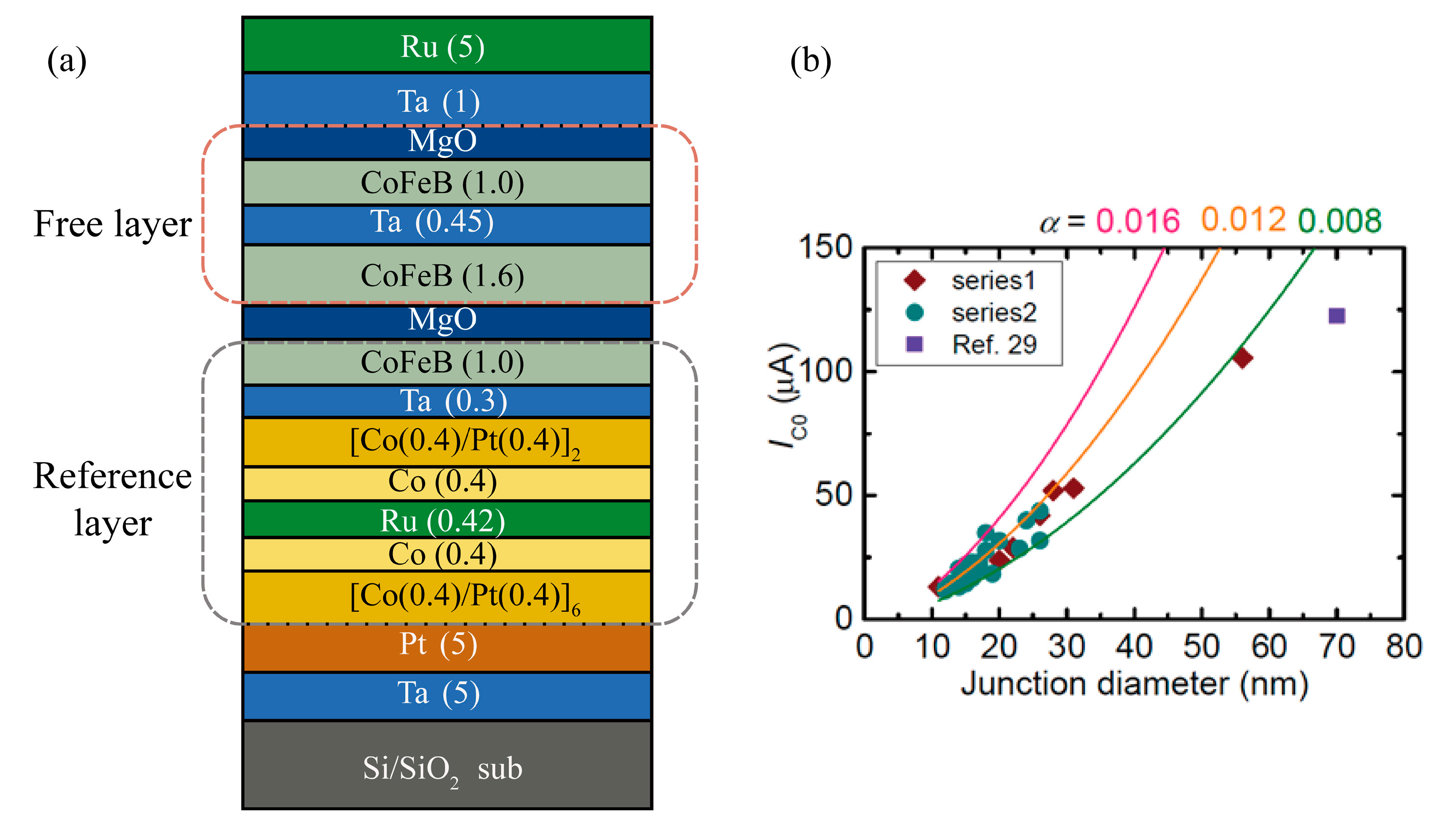
5.2. Structure Optimization: Double CoFeB/MgO Interfaces

Since PMA mainly originates from CoFeB/MgO interface, the idea of improving PMA using multiple interfaces is reasonable. With carefully tuned MgO oxidation, the MgO/CoFeB/MgO layer fabricated by TDK-Headway Technologies Inc. (Milpitas, CA, USA) in 2012 demonstrated low RA of 6.6 Ω·μm2, which is similar to that of Ta film capped structure, while retaining a TMR ratio of 102%. This is the first time that low switching current (45% decrease) and high interfacial PMA have been achieved simultaneously with double oxidation interfaces [50].
The same year, Sato et al. [51] investigated MTJ with MgO/CoFeB/Ta/CoFeB/MgO free layer containing double CoFeB/MgO interfaces, which exhibited high thermal stability and comparable threshold currents. The thickness of Ta spacer layer was designed as 0.4 nm for the top and bottom CoFeB layers to form large enough exchange coupling, enabling the simultaneous STT switching of the two layers. In Figure 6a, the combination between double CoFeB/MgO interfaces and ultra-thin Co/Pt multilayer based synthetic ferrimagnetic (SyF) reference layer, which has demonstrated suppressed exchange bias and high thermal stability, has further improved the properties of PMA based MTJ [52]. Thus, the junction diameter can be scaled down to 1X nm, with Δ maintaining almost constant value 85 when the diameter is larger than 30 nm, below which it starts to decline [53]. As shown in Figure 6b, threshold current decreases monotonously with scaled device area. Blanket film based calculations attribute the tendencies to the nucleation and single domain type magnetization reversals conversion, as well as the decreasing effective damping constant.
Figure 6. (a) Perpendicular magnetic anisotropy (PMA) MTJ with double CoFeB/MgO interfaces and ultra-thin Co/Pt multilayer based synthetic ferrimagnetic (SyF) reference layer, which has demonstrated suppressed exchange bias and high thermal stability. [53] (b) Average threshold current with respect to junction diameter down to 1X nm (Reproduced with permission from Ikeda et al. [53], International Electron Devices Meeting (IEDM); published by IEEE, 2014).
Micromachines 06 01023 g006

6. Recent Progress and Future Applications

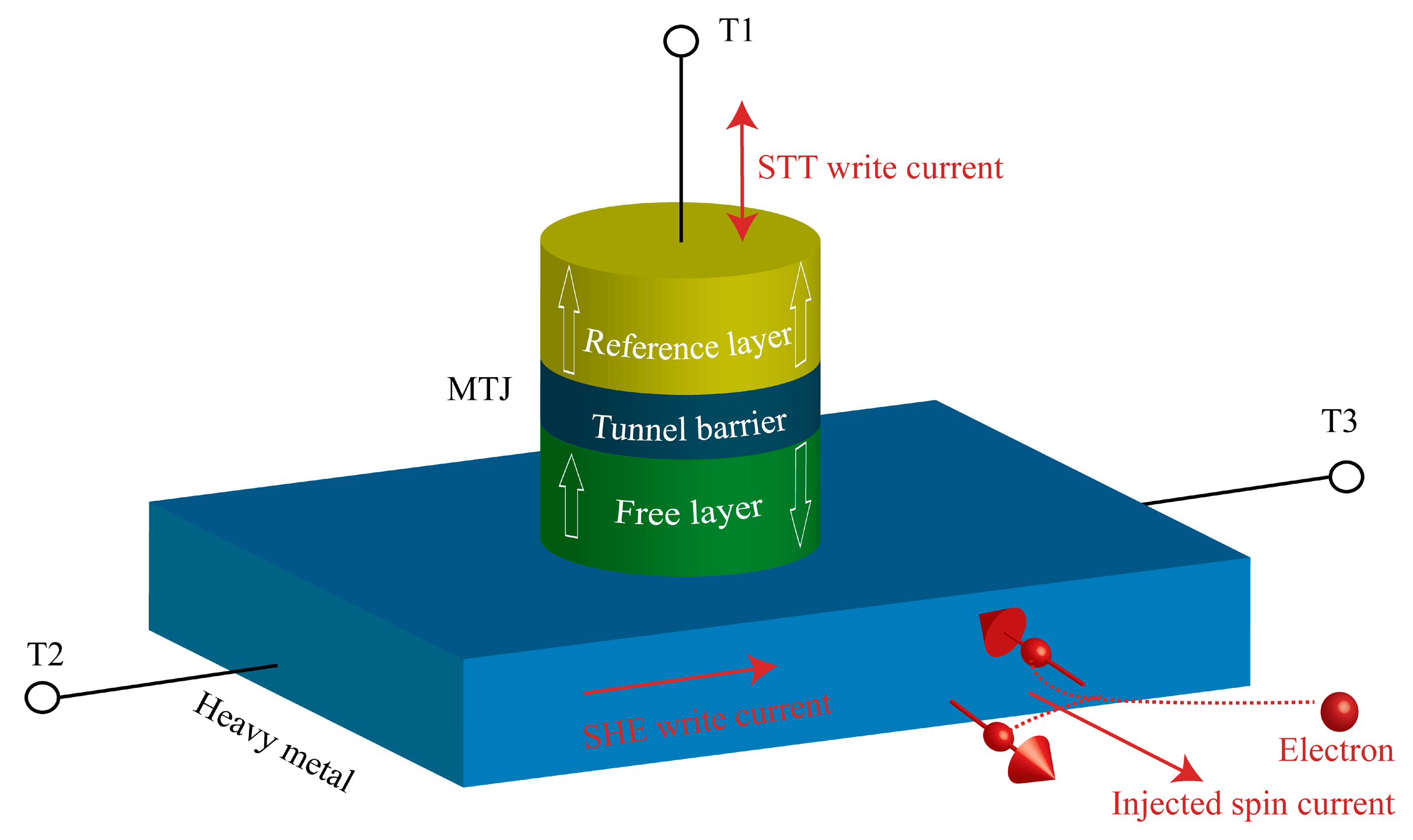
6.1. Spin Orbit Coupling Induced Magnetization Reversal

STT-MRAM has been through a rapid development since its first proposal and demonstration. As the MTJ scales, thinner MgO tunnel barriers are required for lower RA to remain comparable with the transistor, which contradicts the improvement of TMR ratio in the material point of view. Besides, the aging and even breakdown of ultra-thin MgO tunnel barriers caused by writing current passing through the MTJ stack leads to retention and reliability issues of conventional STT-MRAM [54].
To address these concerns, spin orbit torque (SOT), involving spin orbit coupling (SOC) such as spin Hall effect (SHE) or interface effects, has been investigated to realize magnetization rotation and novel devices recently. Figure 7 shows the three-terminal device designed from SOT (SOT-MRAM), where the in-plane writing current is injected through the nonmagnetic film (e.g., Pt, β-Ta, and β-W) on the bottom, generating a transverse spin current to induce quick magnetization reversal of adjacent ferromagnetic layer; the MTJ nano-pillar on the top is used for reading operation referring to its magnetoresistance [55,56,57]. The write path is decoupled from the read path without spin current flowing past the MgO tunnel barrier, which means the properties can be independently tuned. Since the threshold current density to perform SOT based magnetization reversal is nearly constant, competitive power consumption can be expected by reducing the cross-section area of nonmagnetic film, or increasing the material dependent spin Hall angle. The expression of spin Hall angle is θSH = Js/Je , which characterizes the transmission efficiency from charge current density (Je) to spin current density (JS). Following the study of transition metals in high resistivity phase, large spin Hall angle of 0.3 has been found in β-W [57].
Figure 7. Mechanism of the spin Hall effect (SHE) assisted STT switching in PMA MTJ based three-terminal device. SHE write current is injected from terminal T2 and T3 into β-W strap or other heavy metal on the bottom, while the STT write current from terminal T1 penetrates the nano-pillar. Magnetization direction of the free layer can be reversed in absence of external magnetic field.
Micromachines 06 01023 g007
Naturally, the research upon SOT has been concentrated on its application towards MTJ devices with interfacial PMA for its advantages as previously noted. However, in this geometry, an external in-plane magnetic field must be added to assist SOT induced magnetization reversal, which brings negative influence on device fabrication and thermal stability [58]. In 2014, Yu et al. [59] replaced the external magnetic field with lateral structural inversion asymmetry by creating a gradient of TaOx tunnel barrier thickness and oxidation. However, the fabrication of TaOx wedge is not practical in application. Another possible method to cancel additional magnetic field is combining SOT (SHE) and STT, which has been theoretically validated by Brink et al. [60] and Wang et al. [61] using Landau-Lifshitz-Gilbert (LLG) equation. It has been demonstrated that a SHE writing current with 0.5 ns pulse duration allows fast switching speed (1 ns) using a relatively low STT writing current. Additional progress can be made if the interfacial PMA of MTJ with CoFeB/MgO structure is reinforced simultaneously. Similar to the discussion before, an ultra-thin spacer layer made of materials that generate strong interfacial PMA as capping or buffer layers is inserted between the nonmagnetic and magnetic films, e.g., the W/Hf/CoFeB/MgO multilayer, allowing the adjustment of both this parameter and spin Hall angle [62].

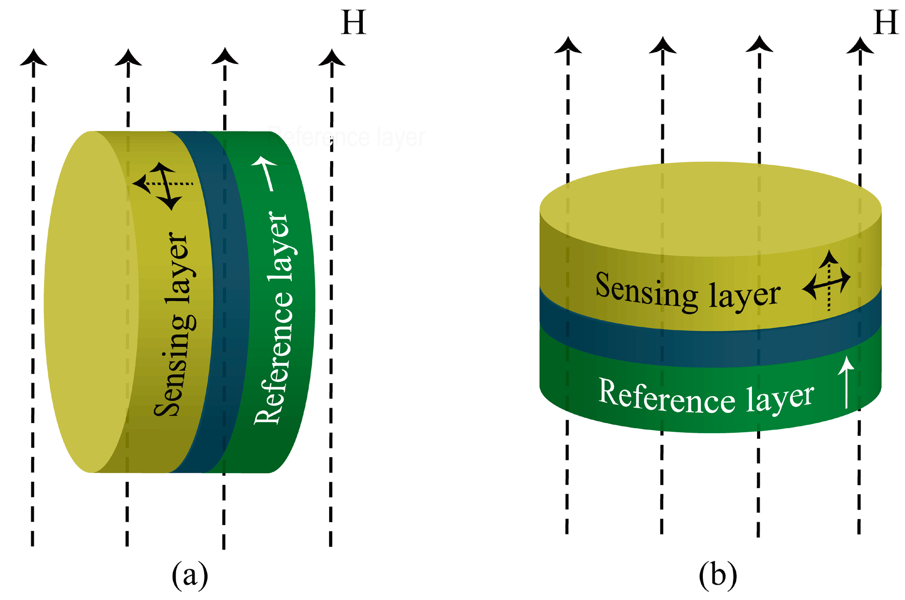
6.2. Perpendicular Magnetic Anisotropy for Magnetic Field Sensor

Magnetoresistance sensor based on MTJ with in-plane magnetic anisotropy has been applied in a wide range of areas, e.g., biosensor and magnetic field sensor. For magnetic field sensor, the magnetization direction of sensing layer, i.e., free layer, should align orthogonally to that of the reference layer for large sensitivity and linear magnetoresistance response with minimum hysteresis. Thus, two successive annealing procedures at different temperatures under crossed external magnetic fields are required for fabrication, and the magnetization direction of the sensing layer can be rotated during the second procedure for its lower blocking temperature [63,64]. The complicated configuration and processing make it difficult to integrate such magnetic field sensors on Si chip. This problem is aggravated in the case of perpendicular magnetic field sensor.
Thanks to the introduction of PMA MTJ, linear response can be achieved with the coupling between out-of-plane and in-plane magnetization directions of sensing and reference layer [65]. As shown in Figure 8a, when a perpendicular magnetic field is applied, the magnetization direction of the free layer is pulled from out-of-plane to parallel or antiparallel to that of reference layer, along with the linear change of magnetoresistance. The perpendicular easy axis of sensing layer is generated from CoFe layer pinned with CoFe/Pt multilayer, while its formation is completely natural without additional thermal processing. Another kind of perpendicular magnetic field sensor based on CoFeB/MgO interface has been proposed by Lee et al. [66] in 2015. Because of the opposite magnetization direction situation as illustrated in Figure 8b, perpendicular magnetic field can be characterized with linear magnetoresistance response without rotating the position of sensor. It should be mentioned that its sensitivity is held to 0.3%/Oe within a dynamic range of ±25 Oe, which needs to be further improved in comparison with in-plane magnetic anisotropy-based magnetoresistance sensor (2.6%/Oe). All of the parameters, including reference layer coercivity, linear region, and TMR ratio, are independent with various device shapes or areas, thus the performance of sensor can remain designable, stable, and uniform. Additionally, the reference layer coercivity can be manipulated by adjusting the thickness of buffer layer.
Figure 8. Perpendicular magnetic field sensor with (a) out-of-plane and in-plane magnetization direction for sensing and reference layer; (b) the opposite situation. The solid arrow indicate the easy axis, while it orientates to the dash arrow direction in the presence of external magnetic field H.
Micromachines 06 01023 g008
Using PMA is a very convenient method to detect perpendicular magnetic field, whereas the robust PMA is still required to achieve high sensitivity and detectivity. With shortcomings gradually being overcome, PMA MTJ based magnetoresistance sensor provides a potential candidate in magnetic field sensor industry, particularly the versatile sensors for omnidirectional detection and mobile devices.

6.3. Perpendicular Magnetic Anisotropy for Logic Circuits

The increasing static power consumption in CMOS technology beyond 45 nm, as well as the interconnection delay caused by long distance data traffic, also limit the development of transistor based logic circuits. These issues have given rise to logic circuits using the MTJ device. Further promotion is expected when concerning PMA based MTJs.
Logic-in-memory architecture built with hybrid MTJ/CMOS logic circuits, where memory devices are merged into a logic circuit, has drawn considerable attention recently [67,68]. This structure is configured with a write circuit for memory programming, a volatile logic block using MOS transistors, a sense amplifier (S.A) for logic result evaluation, and a non-volatile memory block (e.g., MRAM) for instant data storage. Because of the tricky circuit layout, interconnection distance is shortened for both high access speed and low power consumption. One typical example is the magnetic flip-flop (MFF) shown in Figure 9a [69,70]. Bidirectional current is generated by two nMOS (MN2-3) and two pMOS (MP4-5) transistors when two of them are active, thus the two complementary PMA based MTJ devices perform STT switching and store the result. MN0-1, MP0-3, and MN4 transistors constitute a precharge sense amplifier as the master register in coordination with the slave resister for output. Simulation undertaken with PMA MTJ compact model has proven the feasibility of this MFF. Logic-in-memory architecture demonstrates instant on/off capacity, zero standby power consumption, and immunity to power failure, whereas it still suffers from certain drawbacks: in comparison with MOS logic circuit, the large switching latency of MTJ device limits its computing frequency to the order of GHz; S.A mismatch and intrinsic stochastic switching due to thermal fluctuation cause the of sense reliability degradation. Therefore, progress can be reasonably expected form the further study towards based MTJ.
Actually, the MTJ in previous logic circuits is only used in memory rather than logic block for data storage, thus the extra lateral circuits offset the advantages of MTJs, e.g., scalability. A more intrinsic way to build logic-in-memory circuit is proposed as stateful logic: the MTJ serves as both logic gate and memory element [71]. For instance, the three-input logic device shown in Figure 9b can perform fundamental AND, OR, NAND, NOR and Majority functions with a single MTJ, where the current directions and resistance states denote “1” (“0”) for inputs and outputs respectively [72]. Direct information communication between MTJs is realized by domain wall motion through nano-magnetic channel, enabling more complicated logic function with arithmetic logic unit (ALU).
More aggressively, when spin current is completely applied for input, logic function, data storage, information communication, and output, repeated spin-to-charge conversion can be eliminated for circuit simplification and energy reduction. This is the concept of all spin logic gates: charge current is spin polarized by magnetization direction of input magnet, then the spin current is routed through the channel towards output magnet, and determines its final statement by STT switching [73]. The channel material can comprise metal (e.g., Cu) or semiconductor, while graphene channel is preferred for its long spin diffusion length over 100 μm [74]. Taking advantage of both PMA based MTJ and graphene channel, Su et al. [75] proposed a novel all spin logic device, with which the AND (OR) gate is configured as Figure 10 shown. In this gate, magnetization direction of each input MTJ A, B, and C is controlled with bias voltages, while the sum of modulated spin currents decides whether the magnetic moment of output MTJ can be reversed. Finally, the resistance state is read with another bias voltage. Although simulation has confirmed, the attractive prospect of all spin logic by demonstrating its concatenability, nonlinearity, feedback elimination, gain, and a complete set of Boolean operations, much work is still required to bring this concept into reality.
Figure 9. (a) Magnetic flip-flop (MFF) built with PMA MTJ devices and MOS transistors for logic-in-memory architecture. (b) The three-input logic device to realize stateful logic. When top electrode D, E, and F are grounded, the device executes AND/OR functions under the control of input C. Total current from input A, B, and C should be less than the breakdown current.
Micromachines 06 01023 g009
Figure 10. All spin logic gate AND/OR built with PMA-based MTJs. Data is communicated through bottom graphene channels in the form of spin current injected from input MTJ A, B, and C, of which the sum induces the STT switching in the output MTJ.
Micromachines 06 01023 g010

7. Conclusion and Perspective

This review states advantages, drawbacks and corresponding solutions with respect to PMA-based MTJs. It can be confirmed that the PMA MTJ is indeed a promising candidate to realize low-power computing and other meaningful applications. Meanwhile, great efforts have been made in the last few years for the achievement of robust interfacial PMA in CoFeB/MgO system, including the research upon material and fabrication. Considering that the progress of a PMA MTJ is still in its young stage, we can positively expect improvements in terms of thermal stability, power consumption, switching speed, and thermal endurance. In addition, other potential mechanisms (e.g., SOT) relevant to PMA MTJ and their applications are worth further developing.

Acknowledgments

The authors gratefully acknowledge the International Collaboration Project 2015DFE12880 from the Ministry of Science and Technology in China, and National Natural Science Foundation of China (Grant No. 61471015) for their financial support of this work.

Author Contributions

Mengxing Wang wrote the main part of manuscript. Yue Zhang performed the simulations with PMA MTJ compact model. Xiaoxuan Zhao wrote the part of magnetoresistance sensor and prepared the figures. Weisheng Zhao supervised the work and edited the manuscript.

Conflicts of Interest

The authors declare no conflict of interest.

References

  1. International Technology Roadmap for Semiconductor (ITRS), 2010 Update. Available online: http://www.itrs.net (accessed on 27 March 2014).
  2. Chappert, C.; Fert, A.; Van Dau, F.N. The emergence of spin electronics in data storage. Nat. Mater. 2007, 6, 813–823. [Google Scholar]
  3. Nikonov, D.E.; Young, I. Overview of beyond-CMOS devices and a uniform methodology for their benchmarking. Proc. IEEE 2013, 101, 2498–2533. [Google Scholar]
  4. Wang, D.; Nordman, C.; Daughton, J.M.; Qian, Z.; Fink, J. 70% TMR at room temperature for SDT sandwich junctions with CoFeB as free and reference layers. IEEE Trans. Magn. 2004, 40, 2269–2271. [Google Scholar]
  5. Yuasa, S.; Nagahama, T.; Fukushima, A.; Suzuki, Y.; Ando, K. Giant room-temperature magnetoresistance in single-crystal Fe/MgO/Fe magnetic tunnel junctions. Nat. Mater. 2004, 3, 868–871. [Google Scholar] [PubMed]
  6. Parkin, S.S.P.; Kaiser, C.; Panchula, A.; Rice, P.M.; Hughes, B.; Samant, M.; Yang, S.H. Giant tunnelling magnetoresistance at room temperature with MgO (100) tunnel barriers. Nat. Mater. 2004, 3, 862–867. [Google Scholar] [PubMed]
  7. Ikeda, S.; Hayakawa, J.; Ashizawa, Y.; Lee, Y.M.; Miura, K.; Hasegawa, H.; Tsunoda, M.; Matsukura, F.; Ohno, H. Tunnel magnetoresistance of 604% at 300 K by suppression of Ta diffusion in CoFeB/MgO/CoFeB pseudo-spin-valves annealed at high temperature. Appl. Phys. Lett. 2008, 93, 082508. [Google Scholar] [CrossRef]
  8. Thomas, L.; Jan, G.; Zhu, J.; Liu, H.; Lee, Y.J.; Le, S.; Tong, R.Y.; Pi, K.; Wang, Y.J.; Shen, D.; et al. Perpendicular spin transfer torque magnetic random access memories with high spin torque efficiency and thermal stability for embedded applications. J. Appl. Phys. 2014, 115, 172615. [Google Scholar] [CrossRef]
  9. Kent, A.D.; Worledge, D.C. A new spin on magnetic memories. Nat. Nanotech. 2015, 10, 187–191. [Google Scholar] [CrossRef]
  10. Carcia, P.F.; Meinhaldt, A.D.; Suna, A. Perpendicular magnetic anisotropy in Pd/Co thin film layered structures. Appl. Phys. Lett. 1985, 47, 178–180. [Google Scholar] [CrossRef]
  11. Carcia, P.F. Perpendicular magnetic anisotropy in Pd/Co and Pt/Co thin-film layered structures. J. Appl. Phys. 1988, 63, 5066–5073. [Google Scholar] [CrossRef]
  12. Hashimoto, S.; Ochiai, Y.; Aso, K. Perpendicular magnetic anisotropy and magnetostriction of sputtered Co/Pd and Co/Pt multilayered films. J. Appl. Phys. 1989, 66, 4909–4916. [Google Scholar] [CrossRef]
  13. Park, J.H.; Park, C.; Jeong, T.; Moneck, M.T.; Nufer, N.T.; Zhu, J.G. Co/Pt multilayer based magnetic tunnel junctions using perpendicular magnetic anisotropy. J. Appl. Phys. 2008, 103, 07A917. [Google Scholar] [CrossRef]
  14. Lim, D.; Kim, K.; Kim, S.; Jeung, W.Y.; Lee, S.R. Study on exchange-biased perpendicular magnetic tunnel junction. IEEE Trans. Magn. 2009, 45, 2407–2409. [Google Scholar]
  15. Yakushiji, K.; Saruya, T.; Kubota, H.; Fukushima, A.; Nagahama, T.; Yuasa, S.; Ando, K. Ultrathin Co/Pt and Co/Pd superlattice films for MgO-based perpendicular magnetic tunnel junctions. Appl. Phys. Lett. 2010, 97, 232508. [Google Scholar] [CrossRef]
  16. Ishikawa, S.; Sato, H.; Yamanouchi, M.; Ikeda, S.; Fukami, S.; Matsukura, F.; Ohno, H. Magnetic properties of MgO-[Co/Pt] multilayers with a CoFeB insertion layer. J. Appl. Phys. 2013, 113, 17C721. [Google Scholar] [CrossRef]
  17. Mizunuma, K.; Ikeda, S.; Park, J.H.; Yamamoto, H.; Gan, H.; Miura, K.; Hasegawa, H.; Hayakawa, J.; Matsukura, F.; Ohno, H. MgO barrier-perpendicular magnetic tunnel junctions with CoFe/Pd multilayers and ferromagnetic insertion layers. Appl. Phys. Lett. 2009, 95, 232516. [Google Scholar] [CrossRef]
  18. Lee, C.M.; Ye, L.X.; Hsieh, T.H.; Huang, C.Y.; Wu, T.H. Magnetic properties of TbFeCo-based perpendicular magnetic tunnel junctions. J. Appl. Phys. 2010, 107, 09C712. [Google Scholar] [CrossRef]
  19. Ikeda, S.; Miura, K.; Yamamoto, H.; Mizunuma, K.; Gan, H.D.; Endo, M.; Kanai, S.; Hayakawa, J.; Matsukura, F.; Ohno, H. A perpendicular-anisotropy CoFeB–MgO magnetic tunnel junction. Nat. Mater. 2010, 9, 721–724. [Google Scholar] [CrossRef] [PubMed]
  20. Zhao, W.S.; Zhang, Y.; Devolder, T.; Klein, J.O.; Ravelosona, D.; Chappert, C.; Mazoyer, P. Failure and reliability analysis of STT-MRAM. Microelectron. Reliab. 2012, 52, 1848–1852. [Google Scholar] [CrossRef]
  21. Shimabukuro, R.; Nakamura, K.; Akiyama, T.; Ito, T. Electric field effects on magnetocrystalline anisotropy in ferromagnetic Fe monolayers. Physica E Low-Dimens. Syst. Nanostruct. 2010, 42, 1014–1017. [Google Scholar] [CrossRef]
  22. Yang, H.X.; Chshiev, M.; Dieny, B.; Lee, J.H.; Manchon, A.; Shin, K.H. First-principles investigation of the very large perpendicular magnetic anisotropy at Fe|MgO and Co|MgO interfaces. Phys. Rev. B 2011, 84, 054401. [Google Scholar] [CrossRef]
  23. Slonczewski, J.C. Current-driven excitation of magnetic multilayers. J. Magn. Magn. Mater. 1996, 159, L1–L7. [Google Scholar] [CrossRef]
  24. Huai, Y.; Albert, F.; Nguyen, P.; Pakala, M.; Valet, T. Observation of spin-transfer switching in deep submicron-sized and low-resistance magnetic tunnel junctions. Appl. Phys. Lett. 2004, 84, 3118–3120. [Google Scholar] [CrossRef]
  25. Ikeda, S.; Sato, H.; Yamanouchi, M.; Gan, H.; Miura, K.; Mizunuma, K.; Kana, N.; Fukami, S.; Matsukura, F.; Kasai, N.; Ohno, H. Recent progress of perpendicular anisotropy magnetic tunnel junctions for nonvolatile VLSI. Spin 2012, 2, 1240003. [Google Scholar] [CrossRef]
  26. Nakayama, M.; Kai, T.; Shimomura, N.; Amano, M.; Kitagawa, E.; Nagase, T.; Yoshikawa, M.; Kishi, T.; Ikegawa, S.; Yoda, H. Spin transfer switching in TbCoFe/CoFeB/MgO/CoFeB/TbCoFe magnetic tunnel junctions with perpendicular magnetic anisotropy. J. Appl. Phys. 2008, 103, 07A710. [Google Scholar] [CrossRef]
  27. Worledge, D.C.; Hu, G.; Abraham, D.W.; Sun, J.Z.; Trouilloud, P.L.; Nowak, J.; Brown, S.; Gaidis, M.C.; O’Sullivan, E.J.; Robertazzi, R.P. Spin torque switching of perpendicular Ta/CoFeB/MgO-based magnetic tunnel junctions. Appl. Phys. Lett. 2011, 98, 022501. [Google Scholar] [CrossRef]
  28. Zhao, H.; Glass, B.; Amiri, P.K.; Lyle, A.; Zhang, Y.; Chen, Y.J.; Rowlands, G.; Upadhyaya, P.; Zeng, Z.; Katine, J.A.; et al. Sub-200 ps spin transfer torque switching in in-plane magnetic tunnel junctions with interface perpendicular anisotropy. J. Phys. D Appl. Phys. 2012, 45, 025001. [Google Scholar] [CrossRef]
  29. Choi, Y.S.; Nagamine, Y.; Tsunekawa, K.; Maehara, H.; Djayaprawira, D.D.; Yuasa, S.; Ando, K. Effect of Ta getter on the quality of MgO tunnel barrier in the polycrystalline CoFeB/MgO/CoFeB magnetic tunnel junction. Appl. Phys. Lett. 2007, 90, 012505. [Google Scholar] [CrossRef]
  30. Sinha, J.; Gruber, M.; Kodzuka, M.; Ohkubo, T.; Mitani, S.; Hono, K.; Hayashi, M. Influence of boron diffusion on the perpendicular magnetic anisotropy in Ta|CoFeB|MgO ultrathin films. J. Appl. Phys. 2015, 117, 043913. [Google Scholar] [CrossRef]
  31. Gokan, H.; Esho, S. Pattern fabrication by oblique incidence ion-beam etching. J. Vac. Sci. Technol. 1981, 18, 23–27. [Google Scholar] [CrossRef]
  32. Kinoshita, K.; Utsumi, H.; Suemitsu, K.; Hada, H.; Sugibayashi, T. Etching magnetic tunnel junction with metal etchers. Jpn. J. Appl. Phys. 2010, 49, 08JB02. [Google Scholar] [CrossRef]
  33. Kinoshita, K.; Yamamoto, T.; Honjo, H.; Kasai, N.; Ikeda, S.; Ohno, H. Damage recovery by reductive chemistry after methanol-based plasma etch to fabricate magnetic tunnel junctions. Jpn. J. Appl. Phys. 2012, 51, 08HA01. [Google Scholar] [CrossRef]
  34. Vasile, M.J.; Mogab, C.J. Chemically assisted sputter-etching of permalloy using CO or Cl2. J. Vac. Sci. Technol. A 1986, 4, 1841–1849. [Google Scholar] [CrossRef]
  35. Kinoshita, K.; Yamada, K.; Matsutera, H. Reactive ion etching of Fe-Si-Al alloy for thin film head. IEEE Trans. Magn. 1991, 27, 4888–4890. [Google Scholar] [CrossRef]
  36. Nakatani, I. Ultramicro fabrications on Fe-Ni alloys using electron-beam writing and reactive-ion etching. IEEE Trans. Magn. 1996, 32, 4448–4451. [Google Scholar] [CrossRef]
  37. Osada, T.; Doi, M.; Sakamoto, K.; Maehara, H.; Kodaira, Y. Dry etching of magnetic thin film stacks using CO/NH3 and CH3OH gases for tunneling magneto-resistance devices. In Proceedings of 4th International Symposium on Dry Process, Tokyo, Japan, 30 November–1 December 2004; pp. 127–131.
  38. Kinoshita, K.; Honjo, H.; Fukami, S.; Sato, H.; Mizunuma, K.; Tokutome, K.; Murahata, M.; Ikeda, S.; Miura, S.; Kasai, N.; Ohno, H. Process-induced damage and its recovery for a CoFeB–MgO magnetic tunnel junction with perpendicular magnetic easy axis. Jpn. J. Appl. Phys. 2014, 53, 103001. [Google Scholar] [CrossRef]
  39. Greer, A.A.; Gray, A.X.; Kanai, S.; Kaiser, A.M.; Ueda, S.; Yamashita, Y.; Bordel, C.; Palsson, G.; Maejima, N.; Yang, S.H.; et al. Observation of boron diffusion in an annealed Ta/CoFeB/MgO magnetic tunnel junction with standing-wave hard x-ray photoemission. Appl. Phys. Lett. 2012, 101, 202402. [Google Scholar] [CrossRef]
  40. Kurt, H.; Rode, K.; Oguz, K.; Boese, M.; Faulkner, C.C.; Coey, J.M.D. Boron diffusion in magnetic tunnel junctions with MgO (001) barriers and CoFeB electrodes. Appl. Phys. Lett. 2010, 96, 262501. [Google Scholar] [CrossRef]
  41. Mukherjee, S.; Knut, R.; Mohseni, S.M.; Nguyen, T.A.; Chung, S.; Le, Q.T.; Akerman, J.; Persson, J.; Sahoo, A.; Hazarika, A.; et al. Role of boron diffusion in CoFeB/MgO magnetic tunnel junctions. Phys. Rev. B 2015, 91, 085311. [Google Scholar] [CrossRef]
  42. Ikeda, S.; Koizumi, R.; Sato, H.; Yamanouchi, M.; Miura, K.; Mizunuma, K.; Gan, H.; Matsukura, F.; Ohno, H. Boron composition dependence of magnetic anisotropy and tunnel magnetoresistance in MgO/CoFe (B) based stack structures. IEEE Trans. Magn. 2012, 48, 3829–3832. [Google Scholar] [CrossRef]
  43. Cheng, C.W.; Feng, W.; Chern, G.; Lee, C.M.; Wu, T.H. Effect of cap layer thickness on the perpendicular magnetic anisotropy in top MgO/CoFeB/Ta structures. J. Appl. Phys. 2011, 110, 033916. [Google Scholar] [CrossRef]
  44. Miura, Y.; Tsujikawa, M.; Shirai, M. A first-principles study on magnetocrystalline anisotropy at interfaces of Fe with non-magnetic metals. J. Appl. Phys. 2013, 113, 233908. [Google Scholar] [CrossRef]
  45. Liu, T.; Cai, J.W.; Sun, L. Large enhanced perpendicular magnetic anisotropy in CoFeB/MgO system with the typical Ta buffer replaced by an Hf layer. Aip Adv. 2012, 2, 032151. [Google Scholar] [CrossRef]
  46. Lee, D.S.; Chang, H.T.; Cheng, C.W.; Chern, G. Perpendicular magnetic anisotropy in MgO/CoFeB/Nb and a comparison of the cap layer effect. IEEE Trans. Magn. 2014, 50, 1–4. [Google Scholar] [CrossRef]
  47. Liu, T.; Zhang, Y.; Cai, J.W.; Pan, H.Y. Thermally robust Mo/CoFeB/MgO trilayers with strong perpendicular magnetic anisotropy. Sci. Rep. 2014, 4. [Google Scholar] [CrossRef] [PubMed]
  48. An, G.G.; Lee, J.B.; Yang, S.M.; Kim, J.H.; Chung, W.S.; Hong, J.P. Highly stable perpendicular magnetic anisotropies of CoFeB/MgO frames employing W buffer and capping layers. Acta Mater. 2015, 87, 259–265. [Google Scholar] [CrossRef]
  49. Wang, M.; Peng, S.; Zhang, Y.; Zhang, Y.; Zhang, Y.; Zhang, Q.; Ravelosona, D.; Zhao, W. A Multi-Level Cell for STT-MRAM Realized by Capping Layer Adjustment. In Proceedings of the IEEE Magnetics Conference, Beijing, China, 11–15 May 2015.
  50. Jan, G.; Wang, Y.J.; Moriyama, T.; Lee, Y.J.; Lin, M.; Zhong, T.; Tong, R.Y.; Torng, T.; Wang, P.K. High spin torque efficiency of magnetic tunnel junctions with MgO/CoFeB/MgO free layer. Appl. Phys. Express 2012, 5, 093008. [Google Scholar] [CrossRef]
  51. Sato, H.; Yamanouchi, M.; Ikeda, S.; Fukami, S.; Matsukura, F.; Ohno, H. Perpendicular-anisotropy CoFeB-MgO magnetic tunnel junctions with a MgO/CoFeB/Ta/CoFeB/MgO recording structure. Appl. Phys. Lett. 2012, 101, 022414. [Google Scholar] [CrossRef]
  52. Sato, H.; Yamanouchi, M.; Ikeda, S.; Fukami, S.; Matsukura, F.; Ohno, H. MgO/CoFeB/Ta/CoFeB/MgO recording structure in magnetic tunnel junctions with perpendicular easy axis. IEEE Trans. Magn. 2013, 49, 4437–4440. [Google Scholar] [CrossRef]
  53. Ikeda, S.; Sato, H.; Honjo, H.; Enobio, E.C.I.; Ishikawa, S.; Yamanouchi, M.; Fukami, S.; Kanai, S.; Matsukura, F.; Endoh, T.; Ohno, H. Perpendicular-anisotropy CoFeB-MgO based magnetic tunnel junctions scaling down to 1X nm. In Proceedings of the IEEE International Electron Devices Meeting, San Francisco, CA, USA, 15–17 December 2014; pp. 3321–3324.
  54. Amara-Dababi, S.; Sousa, R.C.; Chshiev, M.; Béa, H.; Alvarez-Hérault, J.; Lombard, L.; Prejbeanu, I.L.; Mackay, K.; Dieny, B. Charge trapping-detrapping mechanism of barrier breakdown in MgO magnetic tunnel junctions. Appl. Phys. Lett. 2011, 99, 083501. [Google Scholar] [CrossRef]
  55. Liu, L.; Moriyama, T.; Ralph, D.C.; Buhrman, R.A. Spin-torque ferromagnetic resonance induced by the spin Hall effect. Phys. Rev. Lett. 2011, 106, 036601. [Google Scholar] [CrossRef] [PubMed]
  56. Liu, L.; Pai, C.F.; Li, Y.; Tseng, H.W.; Ralph, D.C.; Buhrman, R.A. Spin-torque switching with the giant spin Hall effect of tantalum. Science 2012, 336, 555–558. [Google Scholar] [CrossRef] [PubMed]
  57. Pai, C.F.; Liu, L.; Li, Y.; Tseng, H.W.; Ralph, D.C.; Buhrman, R.A. Spin transfer torque devices utilizing the giant spin Hall effect of tungsten. Appl. Phys. Lett. 2012, 101, 122404. [Google Scholar] [CrossRef]
  58. Cubukcu, M.; Boulle, O.; Drouard, M.; Garello, K.; Avci, C.O.; Miron, I.M.; Langer, J.; Ocker, B.; Gambardella, P.; Gaudin, G. Spin-orbit torque magnetization switching of a three-terminal perpendicular magnetic tunnel junction. Appl. Phys. Lett. 2014, 104, 042406. [Google Scholar] [CrossRef]
  59. Yu, G.; Upadhyaya, P.; Fan, Y.; Alzate, J.G.; Jiang, W.; Wong, K.L.; Takei, S.; Bender, S.A.; Chang, L.T.; Jiang, Y.; Lang, M.; Tang, J.; Wang, Y.; Tserkovnyak, Y.; Amiri, P.K.; Wang, K.L. Switching of perpendicular magnetization by spin-orbit torques in the absence of external magnetic fields. Nat. Nanotech. 2014, 9, 548–554. [Google Scholar] [CrossRef] [PubMed]
  60. Van den Brink, A.; Cosemans, S.; Cornelissen, S.; Manfrini, M.; Vaysset, A.; Van Roy, W.; Min, T.; Swagten, H.J.M.; Koopmans, B. Spin-Hall-assisted magnetic random access memory. Appl. Phys. Lett. 2014, 104, 012403. [Google Scholar] [CrossRef]
  61. Wang, Z.; Zhao, W.; Deng, E.; Klein, J.O.; Chappert, C. Perpendicular-anisotropy magnetic tunnel junction switched by spin-Hall-assisted spin-transfer torque. J. Phys. D Appl. Phys. 2015, 48, 065001. [Google Scholar] [CrossRef]
  62. Pai, C.F.; Nguyen, M.H.; Belvin, C.; Vilela-Leão, L.H.; Ralph, D.C.; Buhrman, R.A. Enhancement of perpendicular magnetic anisotropy and transmission of spin-Hall-effect-induced spin currents by a Hf spacer layer in W/Hf/CoFeB/MgO layer structures. Appl. Phys. Lett. 2014, 104, 082407. [Google Scholar] [CrossRef]
  63. Negulescu, B.; Lacour, D.; Montaigne, F.; Gerken, A.; Paul, J.; Spetter, V.; Marienb, J.; Duret, C.; Hehn, M. Wide range and tunable linear magnetic tunnel junction sensor using two exchange pinned electrodes. Appl. Phys. Lett. 2009, 95, 112502. [Google Scholar] [CrossRef]
  64. Chen, J.Y.; Feng, J.F.; Coey, J.M.D. Tunable linear magnetoresistance in MgO magnetic tunnel junction sensors using two pinned CoFeB electrodes. Appl. Phys. Lett. 2012, 100, 142407. [Google Scholar] [CrossRef]
  65. Ding, Y.; Judy, J.H.; Wang, J.P. Magneto-resistive sensors with perpendicular magnetic anisotropy. IEEE Trans. Magn. 2005, 41, 707–712. [Google Scholar] [CrossRef]
  66. Lee, Y.C.; Chao, C.T.; Li, L.C.; Suen, Y.W.; Horng, L.; Wu, T.H.; Chang, C.R.; Wu, J.C. Magnetic tunnel junction based out-of-plane field sensor with perpendicular magnetic anisotropy in reference layer. J. Appl. Phys. 2015, 117, 17A320. [Google Scholar] [CrossRef]
  67. Matsunaga, S.; Hayakawa, J.; Ikeda, S.; Miura, K.; Hasegawa, H.; Endoh, T.; Ohno, H.; Hanyu, T. Fabrication of a nonvolatile full adder based on logic-in-memory architecture using magnetic tunnel junctions. Appl. Phys. Express 2008, 1, 091301. [Google Scholar] [CrossRef]
  68. Zhao, W.; Torres, L.; Cargnini, L.V.; Brum, R.M.; Zhang, Y.; Guillemenet, Y.; Guillemenet, Y.; Sassatelli, G.; Lakys, Y.; Klein, J.O.; Etiemble, D.; Ravelosona, D.; Chappert, C. High performance SoC design using magnetic logic and memory. In Proceedings of the IEEE International Conference on Very Large Scale Integration, Hong Kong, China, 3–5 October 2011; pp. 10–33.
  69. Zhao, W.; Belhaire, E.; Chappert, C. Spin-MTJ based non-volatile flip-flop. In Nanotechnology, Proceedings of the IEEE conference, Hong Kong, China, 2–5 August 2007; pp. 399–402.
  70. Zhang, Y.; Zhao, W.; Lakys, Y.; Klein, J.O.; Kim, J.V.; Ravelosona, D.; Chappert, C. Compact modeling of perpendicular-anisotropy CoFeB/MgO magnetic tunnel junctions. IEEE Trans. Electron Devices 2012, 59, 819–826. [Google Scholar] [CrossRef]
  71. Mahmoudi, H.; Sverdlov, V.; Selberherr, S. MTJ-based implication logic gates and circuit architecture for large-scale spintronic stateful logic systems. In Proceedings of the European Solid-State Device Research Conference, Brodeaux, France, 17–21 September 2012; pp. 254–257.
  72. Yao, X.; Harms, J.; Lyle, A.; Ebrahimi, F.; Zhang, Y.; Wang, J.P. Magnetic tunnel junction-based spintronic logic units operated by spin transfer torque. IEEE Trans. Nanotechnol. 2012, 11, 120–126. [Google Scholar] [CrossRef]
  73. Behin-Aein, B.; Datta, D.; Salahuddin, S.; Datta, S. Proposal for an all-spin logic device with built-in memory. Nat. Nanotech. 2010, 5, 266–270. [Google Scholar] [CrossRef] [PubMed]
  74. Dlubak, B.; Martin, M.B.; Deranlot, C.; Servet, B.; Xavier, S.; Mattana, R.; Sprinkle, M.; Berger, C.; De Heer, W.A.; Petroff, F.; et al. Highly efficient spin transport in epitaxial graphene on SiC. Nat. Phys. 2012, 8, 557–561. [Google Scholar] [CrossRef]
  75. Su, L.; Zhao, W.; Zhang, Y.; Querlioz, D.; Zhang, Y.; Klein, J.O.; Dollfus, P.; Bournel, A. Proposal for a graphene-based all-spin logic gate. Appl. Phys. Lett. 2015, 106, 072407. [Google Scholar] [CrossRef]

