Abstract
In this work, cuprous oxide (Cu2O) thin films were prepared using a simplistic sputtering technique. The films were grown on both traditional fluorine-doped tin oxide (FTO) and Ti-metallic substrates. X-ray diffraction applied for investigation of the crystal structure proved that the Cu2O layer acquires the cubic structure with a (111) main peak at 2θ of 36.46°. The optical absorption and transmission were detected through the utilization of a UV-Vis spectrophotometer, and the optical bandgap for the Cu2O layer was determined to be ~2.15 eV using Tauc’s equation. XPS and scanning electron microscopy were also performed for chemical structure and morphological investigation, respectively. The optoelectronic behaviors for the prepared samples were carried out using a Keithley source meter; the photocurrent density was measured in a range of applied voltage between −1 and 1 volt under the illumination of a xenon lamp with a power density of 100 mWcm−2. External quantum efficiency, sensitivity, responsivity, and detectivity were computed using proprietary models based on the experimental data.
1. Introduction
Photodetectors are devices that instantaneously convert light into an electrical signal. They are utilized in a variety of applications, including ozone sensing, biochemical analysis, material identification, and night vision [1]. The absorption of light photons with energy higher than the energy gap of the selected material leads to the excitation of the electrons from valence band levels to the conduction band giving rise to electron-hole pairs. The conversion of the light signal into an electrical pulse is accomplished using this approach. Accordingly, semiconducting materials are intriguing competitors for photodetector applications. For the photodetection process in the range from ultraviolet to infrared wavelength silicon is the dominant material, which is utilized in several applications, such as cameras and other electronic devices [2].
Semiconducting materials with substantially broader bandgaps include ZnO, TiO2, GaN, ZnTe, and ZnS [3,4,5,6,7,8], in addition to copper oxides, and are utilized for the photodetection of ultraviolet rays. The following are some of the most widely used types of copper oxides: Cu4O3 (paramelaconite), cupric oxide (CuO), and cuprous oxide (Cu2O). Paramelaconite represents a meta-stable form of copper oxide, considered an intermediate or transitional compound between CuO and Cu2O. Both CuO and Cu2O are stable forms of copper oxides and have numerous applications as a result of their electrical and optical characteristics [9,10,11]. They are p-type semiconductors with small band gaps that can recognize a wide range of light, including UV, visible, and infrared radiation [12,13].
Cu2O has been a favorable candidate for photodetectors and photovoltaic cells owing to its fascinating structural, magnetic, and optoelectronic properties, such as good carrier mobility and high absorption coefficient. Furthermore, it has high chemical stability in electrolytic solutions, whether acidic or basic, and is a non-toxic material with high abundance in nature. Besides, it exhibits a doping level of NA < 1015 cm−3 and a direct bandgap varying from 2.0 to 2.4 eV, which is better for energy conversion technology advancement [14,15]. Different techniques are utilized for the deposition of Cu2O thin films, including pulsed laser, copper foil oxidation within a thermal technique, chemical bath deposition, electrodeposition, spin coating, and radio frequency (RF) sputtering. Films prepared using RF techniques are characterized by low imperfections, favorable homogeneity, in addition to good coherent and adherent properties [16,17,18]. It is widely utilized in numerous scientific applications, including gas sensors, biosensors, supercapacitors, lithium-ion batteries, photocatalytic dye removal, solar cells, and photoelectrochemical water splitting [19,20,21,22,23,24].
Depositions of Cu2O have been made on a variety of substrates, including stainless steel substrates, soda-lime glass, glass quartz, silicon wafers, polyethylene terephthalate and plastic substrates, fiber glass, and co-fred ceramics substrates [25]. Metallic substrates have reasonable features including high thermal and electrical properties, which makes them interesting to use in various scientific applications [26]. Herein, the research is based on the comparison between the growth of Cu2O thin films on the traditional FTO substrate and metallic titanium on a Mo-glass substrate (Ti/Mo-metal) in photodetection applications. Ti-metal exhibits a low resistivity of 4.2 × 10⁻⁵ Ohm and a large work function of ~4.33 eV; in addition, it represented an excellent Ohmic contact for different semiconductors materials. Thus, the usage of a Ti-metal as a substrate for the growth of semiconductors can offer a conductive path for the charge carriers produced by incident photons, which in turn, improves the effectiveness of carrier extraction [9].
2. Results and Discussion
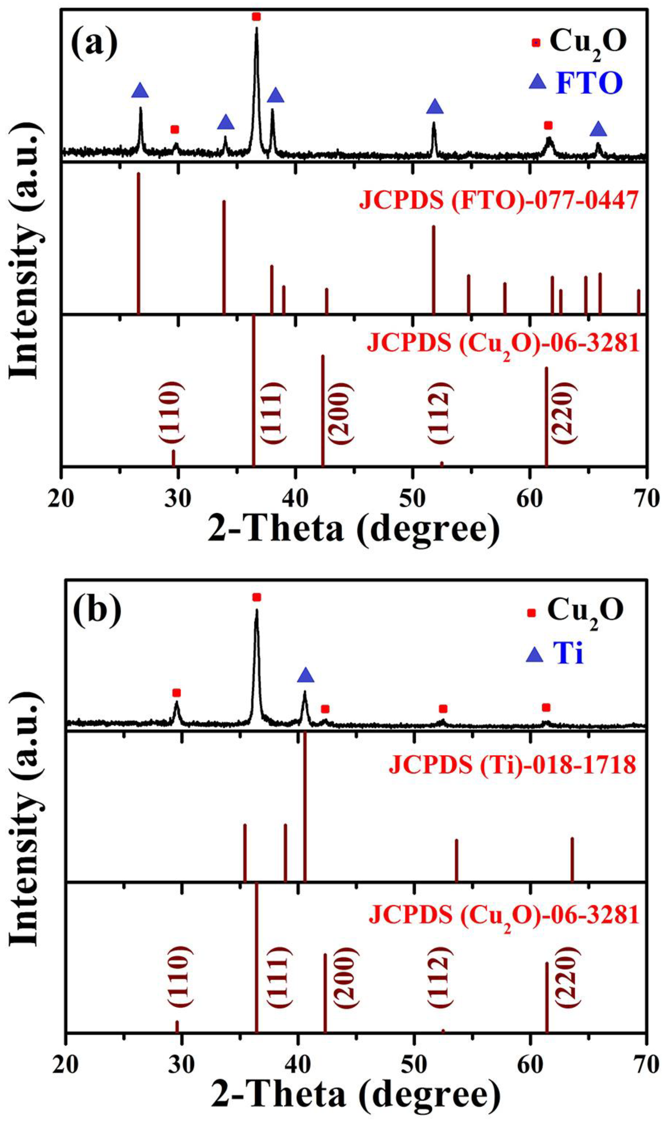
To examine the phase purity, in addition to the crystal structure, Cu2O thin films grown on FTO and Ti-Mo substrates were subjected to X-ray diffraction (XRD) patterns detection. Figure 1a depicts the XRD diffraction patterns belonging to the Cu2O layer deposited on the traditional FTO substrate, three peaks appeared which were assigned to (1 1 0), (1 1 1), and (2 2 0) crystallographic planes as presented in (JCPDS-06-3281) card, the other remaining peaks corresponding to FTO substrate as recorded in (JCPDS-077-0447) card. The most prevalent growth plane for the Cu2O layer is the (1 1 1) plane at 2θ = 36.46 degrees. On the other hand, Figure 1b represents the diffraction patterns in the case of the film deposited on metallic Ti-Mo substrate corresponding to (1 1 0), (1 1 1), (2 0 0), (1 1 2), (2 2 0) crystallographic planes, also the plane (1 1 1) is the main peak as in case of Cu2O grown on FTO glass. The elemental Ti, which emerged from the Ti substrate, is primarily responsible for the peak appearing at 2θ = 40.58 degrees. Following database no. PDF 06-3281, the XRD pattern depicts peaks typical of the cubic structure of Cu2O and a Pn-3 m group space. Additionally, the XRD pattern showed no distinctive peak from CuO or Cu, proving that just Cu2O was produced. In other words, no additional phases developed.
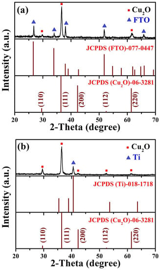
Figure 1.
The XRD diffraction patterns belong to Cu2O layer deposited on (a) traditional FTO and (b) Ti-metallic substrate.
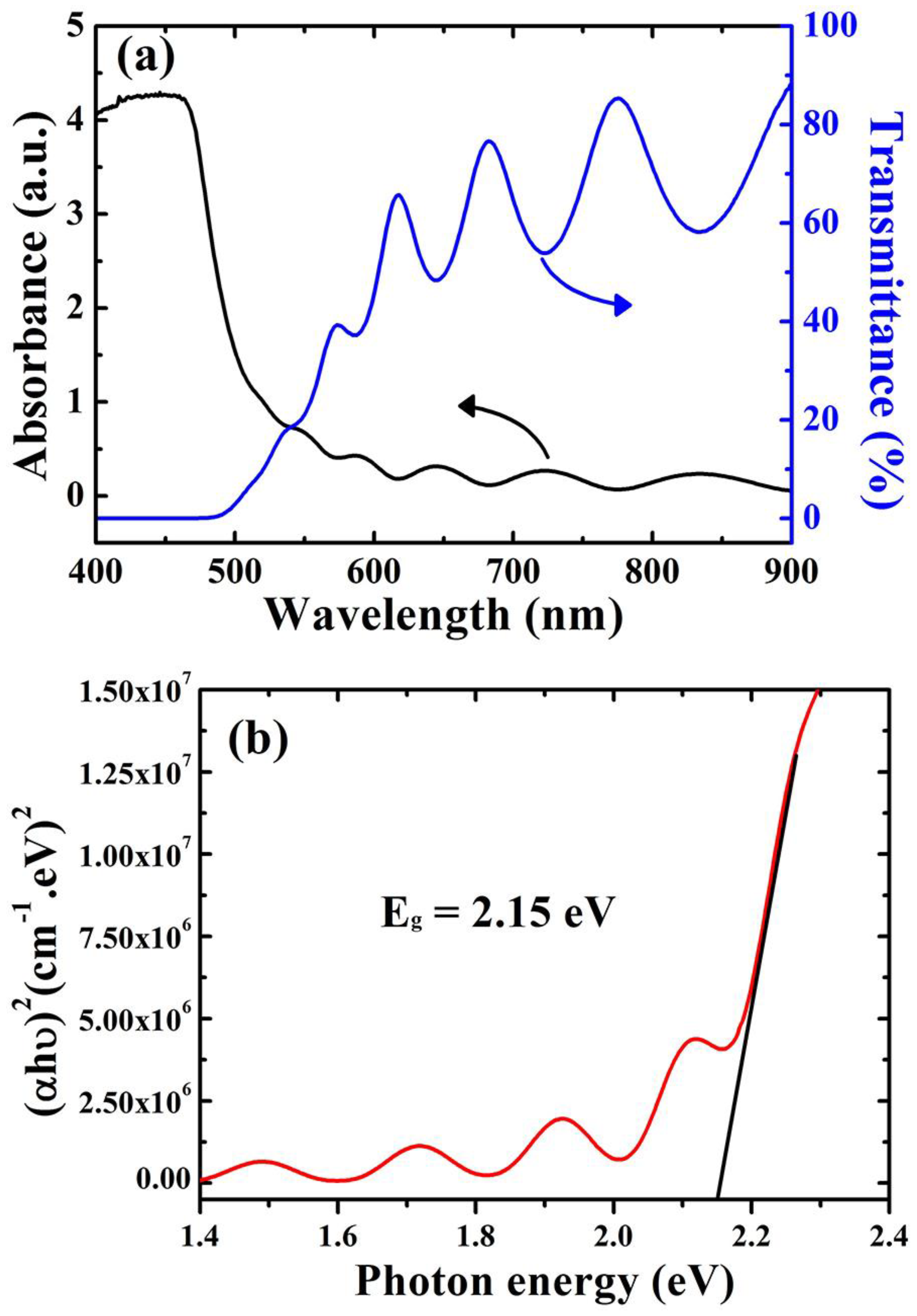
For the detection of optical transmission and absorption, a UV-Vis spectrophotometer is utilized in the range of 400 to 900 nm. As shown in Figure 2a, Cu2O film displayed a high absorption peak up to 450 nm, which corresponds to the visible light spectrum. Furthermore, there was a low-transmission region in the range of 400 to 500 nm and then the transmission increased irregularly from 550 to 900 nm. The transmission value was around 58% at 900 nm, revealing that the deposited Cu2O films exhibit high transparency with respect to IR light. The allowed band gap (Eg) is estimated by using Tauc’s relation, Equation (1) [27].
where B is a constant, ν is the frequency of the incident photon, h is Planck’s constant, and α represents the absorption coefficient. Eg was estimated via the extrapolating of a straight line at the x-axis as shown in Figure 2b. The calculated Eg value was 2.15 eV; this value is very close to the typical value for Cu2O film (2.5 eV). This value makes the deposited films unique for use in solar light exploitation applications, as well as photodetector applications.
(αhν)2 = B (hν − Eg)
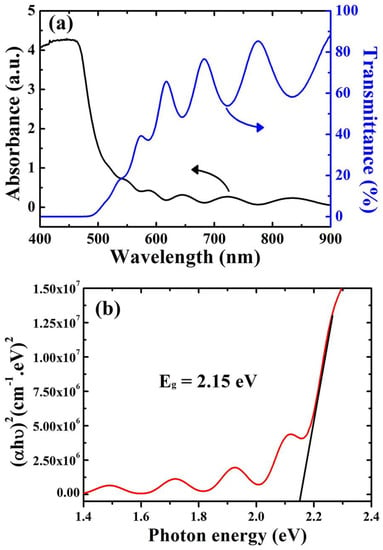
Figure 2.
(a) The optical transmission and absorption of the Cu2O layer. (b) The allowed band gap (Eg) estimated using Tauc’s relation.
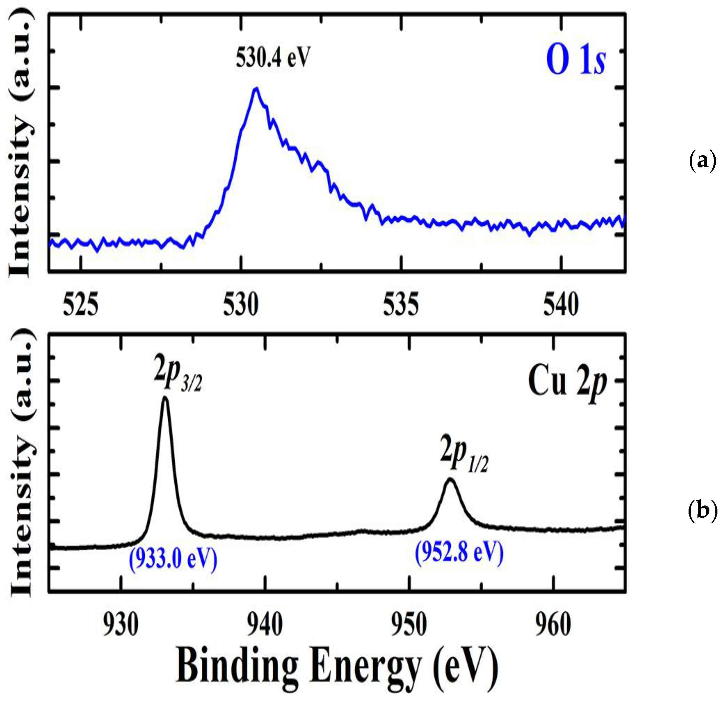
XPS measurements were utilized for the chemical composition of the deposited Cu2O films grown on a Ti-Mo metallic substrate. As seen in Figure 3a, the deconvoluted XPS spectra for oxygen reveal the presence of a signal at 530 eV corresponding to O 1s. The high-resolution spectrum attributed to Cu 2p depicts in Figure 3b, two signals appeared at 933 eV and 952.8 eV, which are attributed to Cu 2p3/2 and Cu 2p1/2. This gives evidence for the presence of Cu2+ in Cu2O film [28]. The sole single phase found is Cu2O, as evidenced by the lack of any distinctive or shake-up satellite peaks connected to Cu2+ species. The XPS results and the XRD data are in agreement with each other.
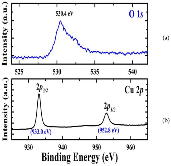
Figure 3.
(a) The deconvoluted XPS spectra for oxygen. (b) The high-resolution spectrum attributed to Cu2p.
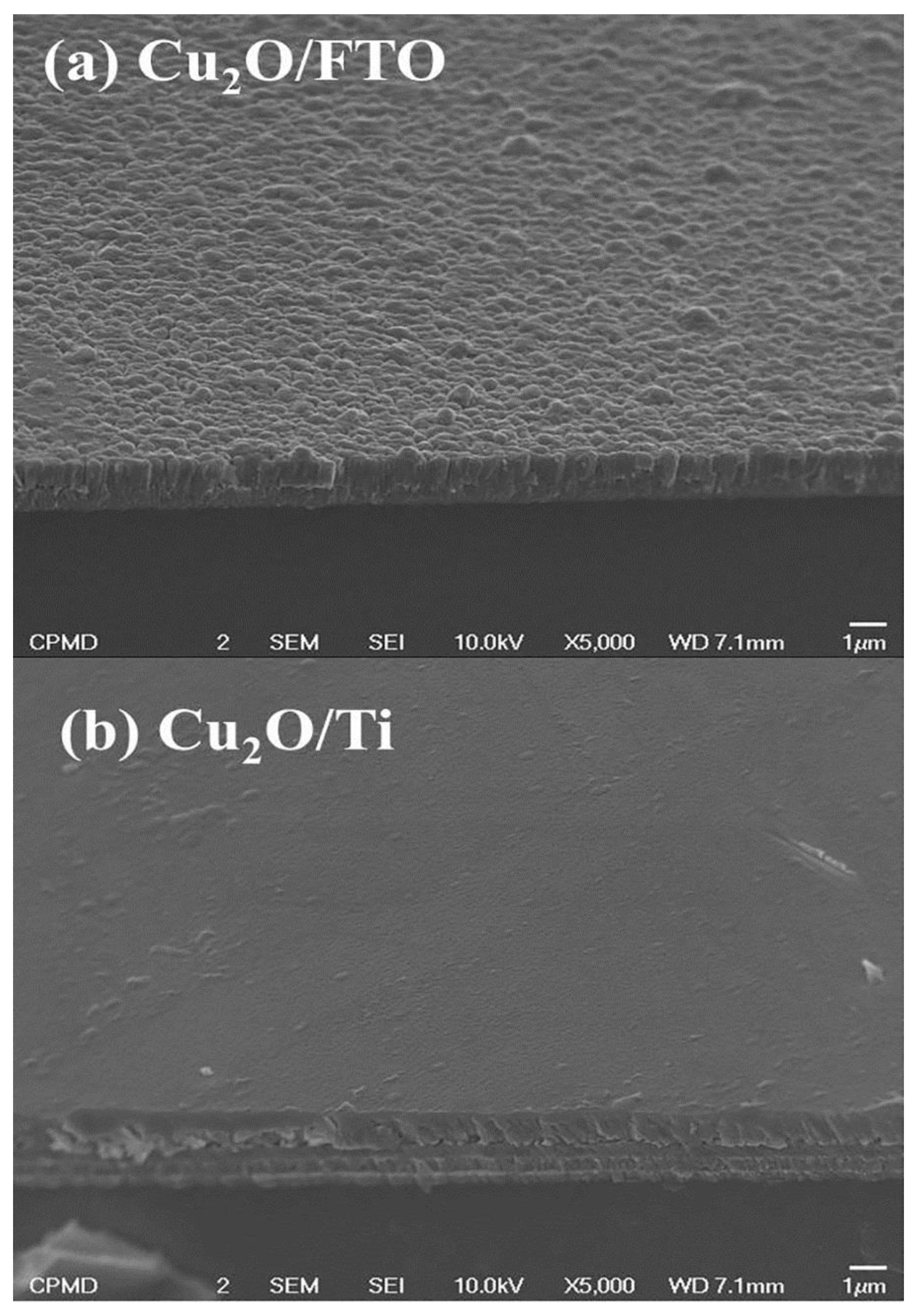
The morphological structure for Cu2O-grown films was detected using FE-SEM. As shown in Figure 4a, Cu2O grown on the traditional FTO substrate initially looked like scattered fragmented particles; it can be described as having a granular structure. Additionally, the existence of observable pinholes on the Cu2O film surface suggests that the FTO substrate does not support sputtering well, which may have an impact on the optical properties and the performance of the deposited film. On the other hand, as depicted in Figure 4b, it is clear that the Cu2O coated on the Ti-metallic wafer appears to be tightly packed and entirely covers the surface of the Ti-Mo substrate. The enhancement of the morphological properties in the case of the Cu2O layer grown on the Ti-Mo substrate could be primarily assigned to better Ohmic contact in addition to the higher electrical conductivity of the metallic substrate, which encouraged the growth of sputtered Cu2O film on its surface. Conversely, the usage of traditional FTO with a lower conductivity leads to suppression of the surface passivation with the Cu2O layer.

Figure 4.
The morphological structure for Cu2O grown on (a) traditional FTO and (b) Ti-metallic substrate.
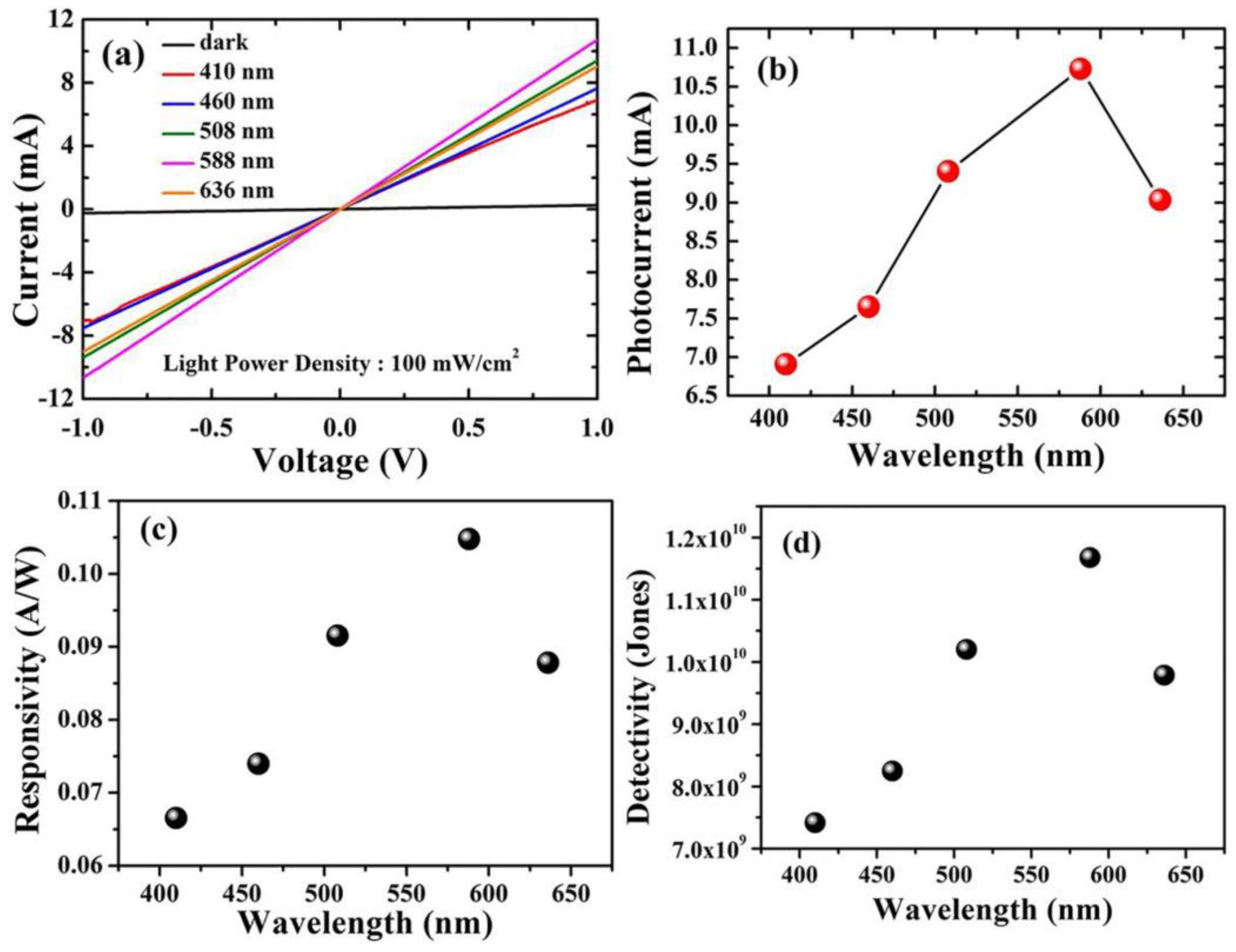
For optoelectronic behavior, the prepared Cu2O samples act as a photodetector and are connected to the Keithley source meter. The response of the samples to incident light was known by measuring the photocurrent density in a voltage range from 1 V to −1 V using different wavelengths. Using the variation of the wavelengths via the utilization of optical filters in the range of 410 nm to 636 nm, the photocurrent is captured at the applied voltage from −1 to 1 volt for both Cu2O layers grown on FTO and Ti-Mo substrate. As shown in Figure 5a, the maximum photocurrent obtained from Cu2O on FTO was around 10 mA at 588 nm, whereas the dark current is comparable to zero. In contrast, as shown in Figure 6a, the Cu2O layer on the Ti-Mo substrate shows an enhancement in the value of the maximum photocurrent where it reaches about 50 mA also at 588 nm. More photocurrent is obtained using Ti-Mo substrate as it can provide a conductive path for the generated electron-hole pair under solar light illumination leading to boosting the carrier separation.
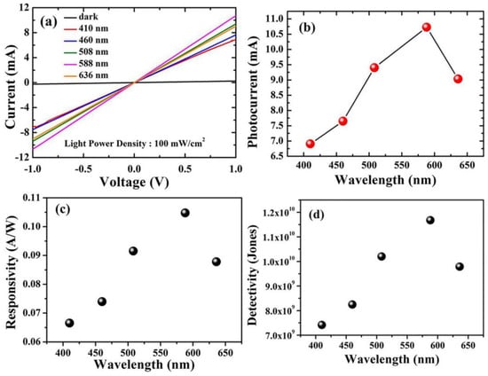
Figure 5.
Optoelectronic characteristics of Cu2O/FTO photodetectors. (a) The photocurrent density at different wavelengths from 410 to 636 nm. (b) The maximum photocurrent density at every wavelength. (c) Responsivity. (d) Detectivity.
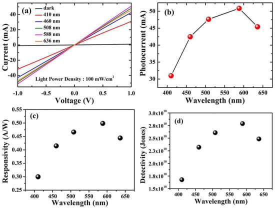
Figure 6.
Optoelectronic characteristics of Cu2O/Ti-Mo photodetectors. (a) The photocurrent density at different wavelengths from 410 to 636 nm. (b) The maximum photocurrent density at every wavelength. (c) Responsivity. (d) Detectivity.
The photodetector responsivity, which indicates the electrical signal that can be generated at a given light power, is defined as the ratio of photocurrent to the power of the illumination source. The responsivity is (Rλ) measured using Equation (2) [29]:
where Iph represents the photocurrent, and P is the power of the illumination source at a specific wavelength. As depicted in Figure 5c, the responsivity of Cu2O grown on FTO varies between 0.065 to 0.11 A/W and the wavelength altered from 410 to 636 nm. The maximum value of R in this case was obtained at 588 nm and reached about 0.11 A/W. In contrast, for the sample deposited on the Ti-Mo substrate, the responsivity exhibits a greater value (~0.50 A/W) also at 588 nm as shown in Figure 6c. The maximum value of the responsivity at 588 nm may be attributed to the higher absorption and the response of the Cu2O to the light falling on it at this wavelength, which matches the optical bandgap as mentioned in Figure 2b.
Rλ = Iph/P (A/W)
The detection ability of the photodetector for weak signals is usually known as the detectivity (D) and it can be measured using the following equation [30]:
where A is the active area, R is the responsivity, e is the charge of the electron, and Id represents the dark current. Moreover, the detectivity for the samples calculated at specific wavelengths from 410 to 636 nm; the general behavior of the detectivity at various wavelengths for Cu2O on FTO and Ti-Mo substrate is completely identical to the behavior of the responsivity as it depends on it as mentioned in Equation (3). The detectivity for Cu2O grown on FTO as shown in Figure 5d varies between 7 × 10⁹ to 1.2 × 10¹⁰ Jones, with the maximum value at 588 nm corresponding to the maximum responsivity at this wavelength. In Figure 6d, the detectivity of Cu2O grown on Ti-Mo substrate exhibited a higher value at 588 nm of 2.8 × 10¹⁰ Jones than the sample deposited the traditional FTO as a result of the higher responsivity of Cu2O than in the case of on Ti-Mo substrate at this wavelength. The previous studies that reported Cu2O as a photodetector are mentioned in Table 1.
D = R √ (A)/√ (2eId) (Jones)

Table 1.
Previous studies reported Cu2O as a photodetector.
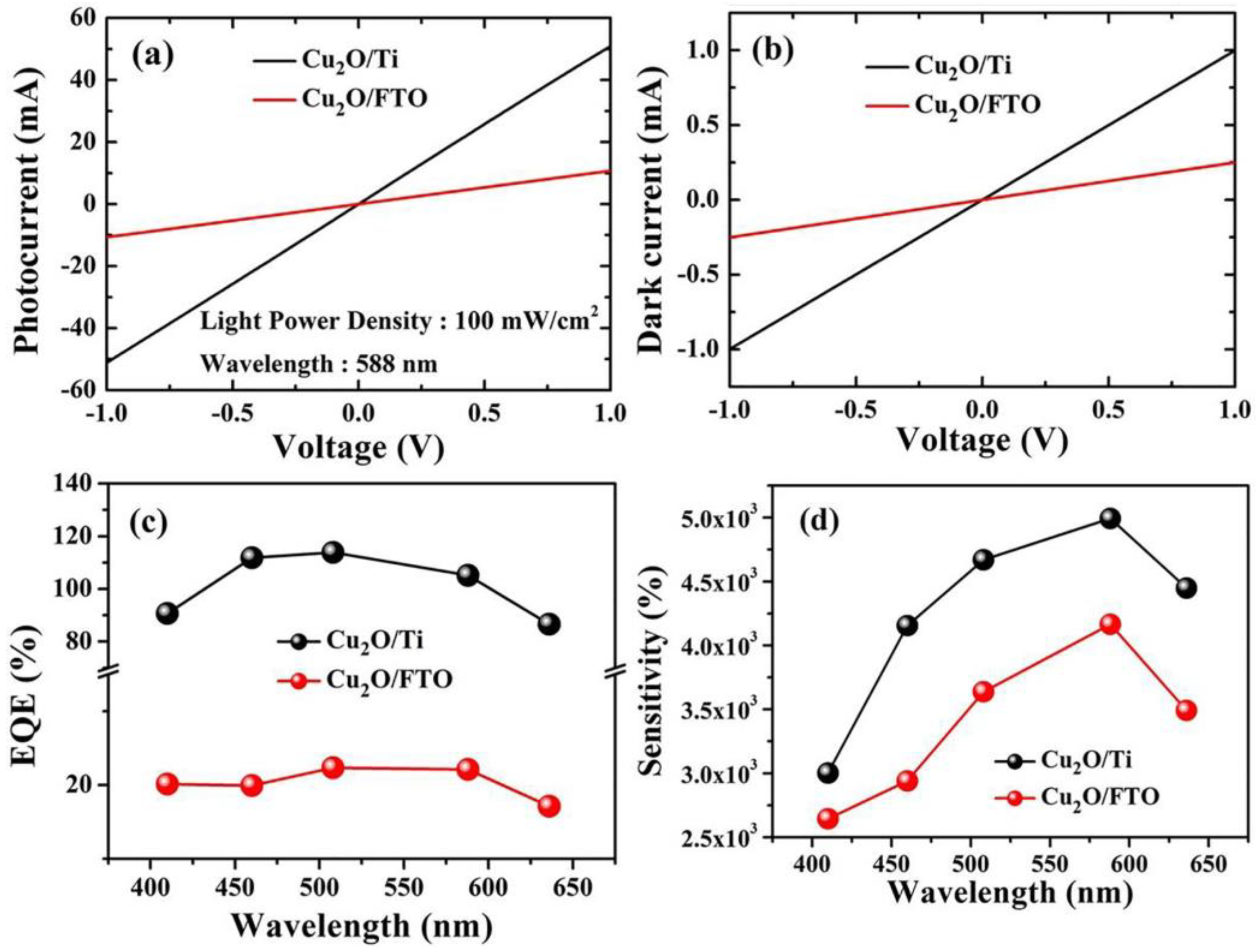
To know the samples’ response to the incident light at the wavelength of 588 nm, a voltage from −1 to 1 volt was applied across both samples while using an optical filter of 588 nm and then the photocurrent was collected in mA as depicted in Figure 7a. For Cu2O/FTO heterojunction, the maximum obtained photocurrent reaches ~10 mA. On the other hand, for Cu2O/Ti, the maximum photocurrent at 588 nm was ~50 mA. This explains the vast difference and the extent to which Ti is superior to FTO as a substrate to obtain more photocurrent. As in Figure 7b, the dark current (Id) was ~1 mA for Cu2O/Ti. It is greater than the dark current in the case of Cu2O/FTO and this is due to the excellent conductive properties of the metallic titanium wafer.
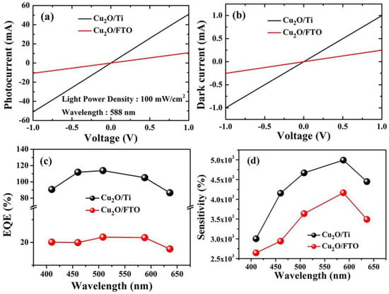
Figure 7.
(a) The samples’ response to the incident light at the wavelength of 588 nm. (b) Dark current for both Cu2O/FTO and Cu2O/Ti samples at an applied voltage from −1 to 1 V. (c) the external quantum efficiency (EQE) at different wavelengths. (d) The variation of the photosensitivity with changing the wavelengths from 410 nm to 636 nm.
The relationship between the generated electrons and the incident light’s photon flux is known as the external quantum efficiency (EQE). The photon flux and light intensity are directly related to each other. According to Equation (4) [38], the R-value is used to calculate the EQE value based on the light wavelength (λ).
EQE = R × (1240/λ) × 100
Figure 7c depicts the calculated values of the EQE at different wavelengths. As shown, for Cu2O/FTO, the maximum value was 20% at 588 nm, whilst for Cu2O/Ti, the maximum value for EQE was around 110% at 450 nm. The proportion of the photocurrent to the dark current can be used to measure the photosensitivity of the prepared photodetectors. The photosensitivity is measured using Equation (5) [39].
where Ip represents the photocurrent and Id is the current without illumination. As seen in Figure 7d, the photosensitivity value varies with changing the wavelengths from 410 nm to 636 nm. Cu2O/FTO has a maximum photosensitivity of 4 × 10³% at 588 nm, whereas the maximum sensitivity for Cu2O/Ti equals 5 × 10³% also at 588 nm. The maximum sensitivity of Cu2O/Ti is greater than Cu2O/FTO because Cu2O/Ti is more responsive to light falling on it and when electrons and holes are generated, electrons have a good conductive path to the external circuit, which leads to an increase in the value of the photocurrent (Ip) and then an increase in the sensitivity.
Photosensitivity = (Ip/Id) × 100
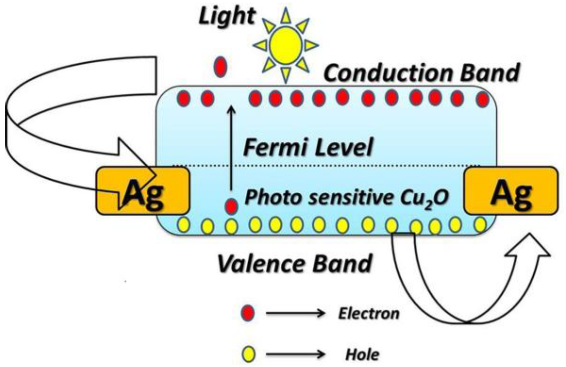
Figure 8 depicts the structure of the band energy of the photodetectors based on Cu2O; it also demonstrates how electron-hole pairs transfer during the illumination process. The following illustration demonstrates how Cu2O works as a photodetector. On the surface of the Cu2O electrode, oxygen molecules are adsorbed in the absence of light and free electrons in the conduction band are, therefore, trapped as shown in Equation (6) [38].
1/2 O2 + 2e2− → O2−

Figure 8.
Schematic diagram depicts the structure of the band energy of the photodetectors based on Cu2O, demonstrating how electron-hole pairs transfer during the illumination process.
This raises the resistance and reduces the current density in dark conditions. Electron-hole pairs form under light irradiation with energy greater than the Eg for the Cu2O layer and, as a result of that, both the photo-induced electrons and holes migrate towards the Ag electrodes. The oxygen ions in this case are desorbed by the holes as they move to the surface, as shown by Equations (7) and (8).
hv → e− + h+
2h+ + O2− → O
The photocurrent rises as the conductivity of Cu2O photoelectrode is increased by the remaining electrons. It is important to shed light on the interpretation of the relationship between the photocurrent and the applied voltage. As depicted in the presented results, the prepared electrodes exhibit a linear or Ohmic behavior for I-V curves. The linearity of I-V curves is attributed to the Ohmic contact between the prepared photoelectrode and the metallic contact deposited on it. The work function of both the semiconductor and the metallic contact determines whether the contact is Ohmic or Schottky. For p-type semiconductors, Schottky contact is formed when its work function is more than the work function of the metallic contact. Herein, Ag past is utilized as a metallic contact for Cu2O photoelectrode. The work function of Cu2O and Ag equal 5 eV and 4.74 eV, respectively, this suggests the formation of a Schottky barrier and, therefore, a non-linear I-V curve. The linear behavior of the I-V curve can be explained as follows, any structural or chemical alterations at the metal-oxide contact should be taken into account, in addition to the work function values. Most metals with low-work functions, such as Ag, are known to reduce Cu2O to create an area of metallic copper (Cu) at the interface. This is connected to the fact that in the presence of oxygen, metallic Ag readily oxidizes (reducing Cu2O) to create stable oxides. Here, Ag was used to coat both sides of the sample, as it acts as an electrical contact to facilitate the transfer of charges generated by light on the Cu2O layer. It is thought that the ensuing oxygen-deficient area at the interface will eventually produce another sort of barrier with characteristics somewhat resembling those of the Cu-Cu2O Ohmic contact [40].
3. Materials and Methods
3.1. Materials and Preparation
First, using an electron beam evaporator (Syskey, Taiwan), 500-nm-thick Ti-metal (99.6%, Sigma Aldrich (St. Louis, MO, USA)) was deposited on a commercial Mo-glass substrate. The cuprous oxide (Cu2O) layer was then deposited on a Ti-coated Mo-glass substrate using an RF sputtering process (AJA-Orion-312RF- sputtering system, Cornel Inc., Scituate, MA, USA). The sputtering target was a 4-inch-diameter copper (I) oxide target (99.999% purity, Kurt J. Lesker Company Ltd., East Sussex, UK). A total of 200 W of RF power was used for 2 h at 5 × 10⁻³ Torr of chamber pressure for the deposition of a 1 µm Cu2O layer. High-purity Argon was used as a sputtering gas at a constant flow rate of 20 standard cubic centimetres per minute. Rapid thermal annealing was utilized for annealing the deposited Cu2O layer in a nitrogen environment for 90 s at 550 °C. For comparison, a layer of Cu2O also was deposited on a traditional FTO substrate (8 Ω/sq, Sigma Aldrich).
3.2. Characterization Techniques
(X’pert PRO, Philips, Eindhoven, Netherlands) diffractometer was utilized for determining the diffraction patterns of the Cu2O deposited films at (1.540598 Å) with a scan rate of 1 min−1 and 2θ from 20:80 degree. Using a (Lambda 950 spectrometer, Perkin-Elmer, Rodgau, Germany) spectrophotometer, the optical behavior for Cu2O films was detected in the range of 400 to 900 nm. The surface morphologies were examined with the aid of field emission scan electron microscope (FE-SEM) (model: JSM-6700F, JEOL, Tokyo, Japan) operated at a voltage of 20 kV. X-ray photoelectron spectroscopy XPSPHI 5000 Versa Probe II (Chanhassen, MN, USA) and the multi-peak computer software version 9, ULVAC-PHI, Inc. (Kanagawa, Japan) were used for determining the elemental composition of the deposited films.
3.3. Photodetection Process Measurements
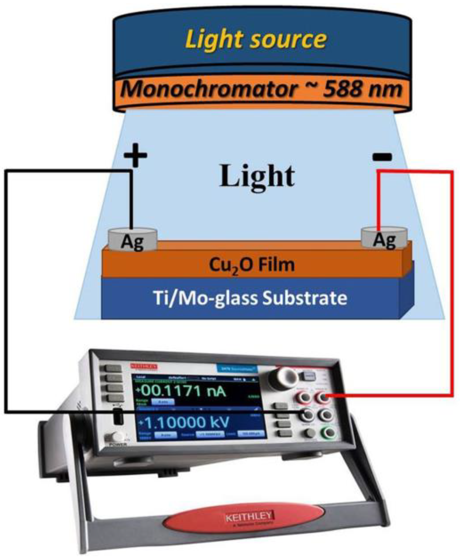
A Keithley source meter (model: 2400, Tektronix Company (Beaverton, OR, USA)) was utilized for investigating the photodetection properties of the prepared Cu2O samples on both FTO and Ti-metallic substrates. The measurements were explored by using a Xenon lamp as a light source (100 mwcm−2) between −1 and + 1 V applied voltage. The fabricated samples with an area of 1 cm2 were connected to two electrodes of the Keithly device via the usage of silver paste performing as an Ohmic contact. The impact of the incident light with diverse wavelengths on the selected sample was detected. External quantum efficiency, sensitivity, responsivity, and detectivity were calculated using custom equations from the experimental data. All testing on the manufacturing samples was done in a standard environment and at ambient temperature. Figure 9 shows the device structure of the Cu2O/Ti/Mo-glass photodetector under light illumination.
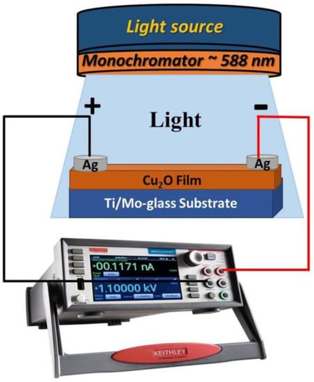
Figure 9.
Schematic diagram of Cu2O/Ti/Mo-glass photodetector under light exposure.
4. Conclusions
Cu2O photosensitive layers grown on FTO and Ti-Mo metallic substrate were used to create a unique optoelectronic photodetector. The facile RF sputtering technique was utilized for the deposition process. The morphological structures for the grown Cu2O/FTO samples appear scattered and fragmented and the pinholes were clearly observed in contrast to the Cu2O/Ti samples, which appear free from pinholes. The diffraction patterns related to the XRD study for both Cu2O/FTO and Cu2O/Ti reveal that the (111) plane appeared as the main peak at around 2θ = 36.46°. The optical bandgap for the Cu2O layer equals 2.15 eV was calculated using Tauc’s relation extracted from the absorption data. The XPS study reveals the attendance of two peaks related to both Cu 2p3/2 and Cu 2p1/2. The prepared photoelectrodes can detect and sense the UV and Vis regions of the electromagnetic spectrum. The optoelectronic behavior for the prepared samples was tested by measuring the photocurrent density under variable wavelengths of illumination from 410 to 636 nm. Cu2O/Ti photoelectrode exhibited more effective optoelectronic properties than Cu2O/FTO photoelectrode. The maximum detectivity and photosensitivity for Cu2O/Ti samples at 588 nm were 2.8 × 10¹⁰ Jones and 5 × 10³%, respectively, whereas the external quantum efficiency was around 110% at 450 nm. The present development is the first step toward realizing mass-scale high-efficiency photodetectors over a wide range of wavelengths for various applications in the future.
Author Contributions
Conceptualization, W.Z.T.; methodology, A.A.; formal analysis, M.S.A.-w., J.K.L., M.M.A.H., B.M.T., A.M.A.-E. and R.I.A.; investigation, W.Z.T., M.M.A.H., B.M.T., A.M.A.-E. and R.I.A.; writing—original draft preparation, A.A. and M.S.A.-w.; writing—review and editing, W.Z.T., J.K.L., A.M.A.-E. and R.I.A.; visualization, A.A. and M.S.A.-w.; supervision, W.Z.T. All authors have read and agreed to the published version of the manuscript.
Funding
The authors extend their sincere appreciation to the Researchers Supporting Project Number (RSPD2023R769), King Saud University, Riyadh, Saudi Arabia for the support.
Data Availability Statement
Data are available within the article.
Conflicts of Interest
The authors declare no conflict of interest.
References
- Li, C.; Li, J.; Li, Z.; Zhang, H.; Dang, Y.; Kong, F. High-performance photodetectors based on nanostructured perovskites. Nanomaterials 2021, 11, 1038. [Google Scholar] [CrossRef]
- Lourenço, M.A.; Milosavljević, M.; Gwilliam, R.M.; Homewood, K.P.; Shao, G. On the role of dislocation loops in silicon light emitting diodes. Appl. Phys. Lett. 2005, 87, 201105. [Google Scholar] [CrossRef]
- Li, Q.; Huang, J.; Meng, J.; Li, Z. Enhanced Performance of a Self-Powered ZnO Photodetector by Coupling LSPR-Inspired Pyro-Phototronic Effect and Piezo-Phototronic Effect. Adv. Opt. Mater. 2022, 10, 2102468. [Google Scholar] [CrossRef]
- Yadav, P.K.; Ajitha, B.; Ahmed, C.M.; Reddy, Y.A.K.; Reddy, V.R.M. Superior UV photodetector performance of TiO2 films using Nb doping. J. Phys. Chem. Solids 2022, 160, 110350. [Google Scholar] [CrossRef]
- Li, Z.; Li, Z.; Zuo, C.; Fang, X. Application of nanostructured TiO2 in UV photodetectors: A review. Adv. Mater. 2022, 34, 2109083. [Google Scholar] [CrossRef]
- Yadav, G.; Gupta, V.; Tomar, M. Double Schottky metal–semiconductor–metal based GaN photodetectors with improved response using laser MBE technique. J. Mater. Res. 2022, 37, 457–469. [Google Scholar] [CrossRef]
- Tawfik, W.Z.; Farghali, A.A.; Moneim, A.; Imam, N.G.; El-Dek, S. Outstanding features of Cu-doped ZnS nanoclusters. Nanotechnology 2018, 29, 215709. [Google Scholar] [CrossRef]
- Suthar, D.; Himanshu; Patel, S.L.; Chander, S.; Kannan, M.D.; Dhaka, M.S. Thickness and annealing evolution to physical properties of e-beam evaporated ZnTe thin films as a rear contact for CdTe solar cells. J. Mater. Sci. Mater. Electron. 2021, 32, 19070–19082. [Google Scholar] [CrossRef]
- Tawfik, W.Z.; Hassan, M.A.; Johar, M.A.; Ryu, S.-W.; Lee, J.K. Highly conversion efficiency of solar water splitting over p-Cu2O/ZnO photocatalyst grown on a metallic substrate. J. Catal. 2019, 374, 276–283. [Google Scholar] [CrossRef]
- Tawfik, W.Z.; Khalifa, Z.S.; Abdel-Wahab, M.S.; Hammad, A.H. Sputtered cobalt doped CuO nano-structured thin films for photoconductive sensors. J. Mater. Sci. Mater. Electron. 2019, 30, 1275–1281. [Google Scholar] [CrossRef]
- Ashour, M.; Abdel-Wahab, M.S.; Shehata, A.; Tawfik, W.Z.; Azooz, M.A.; Elfeky, S.A.; Mohamed, T. Experimental investigation of linear and third-order nonlinear optical properties of pure CuO thin film using femtosecond laser pulses. J. Opt. Soc. Am. B 2022, 39, 508–518. [Google Scholar] [CrossRef]
- Kunturu, P.P.; Huskens, J. Efficient solar water splitting photocathodes comprising a copper oxide heterostructure protected by a thin carbon layer. ACS Appl. Energy Mater. 2019, 2, 7850–7860. [Google Scholar] [CrossRef]
- Bunea, R.; Saikumar, A.K.; Sundaram, K. A comparison of optical properties of CuO and Cu2O thin films for solar cell applications. Mater. Sci. Appl. 2021, 12, 315–329. [Google Scholar]
- Liu, Q.; Tian, H.; Li, J.; Hu, A.; He, X.; Sui, M.; Guo, X. Hybrid graphene/Cu2O quantum dot photodetectors with ultrahigh responsivity. Adv. Opt. Mater. 2019, 7, 1900455. [Google Scholar] [CrossRef]
- Ibrahim, A.M.; Abdel-Wahab, M.S.; Elfayoumi, M.; Tawfik, W.Z. Highly efficient sputtered Ni-doped Cu2O photoelectrodes for solar hydrogen generation from water-splitting. Int. J. Hydrogen Energy 2023, 48, 1863–1876. [Google Scholar] [CrossRef]
- Kartha, C.V.; Rehspringer, J.-L.; Muller, D.; Roques, S.; Bartringer, J.; Ferblantier, G.; Slaoui, A.; Fix, T. Insights into Cu2O thin film absorber via pulsed laser deposition. Ceram. Int. 2022, 48, 15274–15281. [Google Scholar] [CrossRef]
- Derbal, S.; Benaicha, M. Insights on the Effect of Applied Potential on the Properties of Electrodeposited p-Type Cuprous Oxide (Cu2O) Thin Films. J. Electron. Mater. 2021, 50, 5134–5140. [Google Scholar] [CrossRef]
- Abdelhalium, H.H.; Abdel-Wahab, M.S.; Tamm, M.T.; Tawfik, W.Z. Highly efficient ultraviolet photodetector based on molybdenum-doped nanostructured NiO/ITO thin film. Appl. Phys. A 2023, 129, 459. [Google Scholar] [CrossRef]
- Wang, N.; Tao, W.; Gong, X.; Zhao, L.; Wang, T.; Zhao, L.; Liu, F.; Liu, X.; Sun, P.; Lu, G. Highly sensitive and selective NO2 gas sensor fabricated from Cu2O-CuO microflowers. Sens. Actuators B Chem. 2022, 362, 131803. [Google Scholar] [CrossRef]
- Franco, F.F.; Hogg, R.A.; Manjakkal, L. Cu2O-Based Electrochemical Biosensor for Non-Invasive and Portable Glucose Detection. Biosensors 2022, 12, 174. [Google Scholar] [CrossRef]
- Zhang, L.; Li, Q.; Xue, H.; Pang, H. Fabrication of Cu2O-based Materials for Lithium-Ion Batteries. ChemSusChem 2018, 11, 1581–1599. [Google Scholar] [CrossRef] [PubMed]
- Wang, Q.; Zhang, Y.; Xiao, J.; Jiang, H.; Hu, T.; Meng, C. Copper oxide/cuprous oxide/hierarchical porous biomass-derived carbon hybrid composites for high-performance supercapacitor electrode. J. Alloys Compd. 2019, 782, 1103–1113. [Google Scholar] [CrossRef]
- Zhang, C.; Tu, J.; Huang, X.; Yuan, Y.; Chen, X.; Mao, F. Preparation and electrochemical performances of cubic shape Cu2O as anode material for lithium ion batteries. J. Alloys Compd. 2007, 441, 52–56. [Google Scholar] [CrossRef]
- Shi, W.; Zhang, X.; Li, S.; Zhang, B.; Wang, M.; Shen, Y. Carbon coated Cu2O nanowires for photo-electrochemical water splitting with enhanced activity. Appl. Surf. Sci. 2015, 358, 404–411. [Google Scholar] [CrossRef]
- Umar, M.; Swinkels, M.Y.; De Luca, M.; Fasolato, C.; Moser, L.; Gadea, G.; Marot, L.; Glatzel, T.; Zardo, I. Morphological and stoichiometric optimization of Cu2O thin films by deposition conditions and post-growth annealing. Thin Solid Film. 2021, 732, 138763. [Google Scholar] [CrossRef]
- Wölz, M.; Hauswald, C.; Flissikowski, T.; Gotschke, T.; Fernández-Garrido, S.; Brandt, O.; Grahn, H.T.; Geelhaar, L.; Riechert, H. Epitaxial Growth of GaN Nanowires with High Structural Perfection on a Metallic TiN Film. Nano Lett. 2015, 15, 3743–3747. [Google Scholar] [CrossRef]
- Abdelmoneim, A.; Naji, A.; Wagenaars, E.; Shaban, M. Outstanding stability and photoelectrochemical catalytic performance of (Fe, Ni) co-doped Co3O4 photoelectrodes for solar hydrogen production. Int. J. Hydrogen Energy 2021, 46, 12915–12935. [Google Scholar] [CrossRef]
- Zhao, Y.; Zhao, W.; Chen, H.-Y.; Xu, J.-J. Dark-field microscopic real-time monitoring the growth of Au on Cu2O nanocubes for ultra-sensitive glucose detection. Anal. Chim. Acta 2021, 1162, 338503. [Google Scholar] [CrossRef]
- Shaker, S.S.; Ismail, R.A.; Ahmed, D.S. High-Responsivity Heterojunction Photodetector Based on Bi2O3-Decorated MWCNTs Nanostructure Grown on Silicon via Laser Ablation in Liquid. J. Inorg. Organomet. Polym. Mater. 2022, 32, 1381–1388. [Google Scholar] [CrossRef]
- Balakarthikeyan, R.; Santhanam, A.; Anandhi, R.; Vinoth, S.; Al-Baradi, A.M.; Alrowaili, Z.; Al-Buriahi, M.; Kumar, K.D.A. Fabrication of nanostructured NiO and NiO: Cu thin films for high-performance ultraviolet photodetector. Opt. Mater. 2021, 120, 111387. [Google Scholar] [CrossRef]
- Lan, T.; Fallatah, A.; Suiter, E.; Padalkar, S. Size controlled copper (I) oxide nanoparticles influence sensitivity of glucose biosensor. Sensors 2017, 17, 1944. [Google Scholar] [CrossRef]
- Wang, J.; Song, J.; Qin, L.; Peng, Y.; Nötzel, R. Visible-light photoelectrochemical photodetector based on In-rich InGaN/Cu2O core-shell nanowire p–n junctions. Appl. Phys. Lett. 2022, 120, 112108. [Google Scholar] [CrossRef]
- He, C.; Guo, D.; Chen, K.; Wang, S.; Shen, J.; Zhao, N.; Liu, A.; Zheng, Y.; Li, P.; Wu, Z.; et al. α-Ga2O3 Nanorod Array–Cu2O Microsphere p–n Junctions for Self-Powered Spectrum-Distinguishable Photodetectors. ACS Appl. Nano Mater. 2019, 2, 4095–4103. [Google Scholar] [CrossRef]
- Luo, M.; Song, J.; Wang, J.; Pan, X.; Hong, H.; Nötzel, R. Ultraviolet photoelectrochemical photodetector based on GaN/Cu2O core–shell nanowire p–n heterojunctions. AIP Adv. 2022, 12, 115112. [Google Scholar] [CrossRef]
- Duan, Y.; Zhu, Y.; Li, K.; Wang, Q.; Wang, P.; Yu, H.; Yan, Z.; Zhao, X. Cu2O–Au nanowire field-effect phototransistor for hot carrier transfer enhanced photodetection. Nanotechnology 2019, 30, 245202. [Google Scholar] [CrossRef] [PubMed]
- Xu, J.; Cao, Y.; Wei, J.; Sun, J.-L.; Xu, J.; He, J. Solution synthesis of Cu2O/Si radial nanowire array heterojunctions for broadband photodetectors. Mater. Res. Express 2014, 1, 015002. [Google Scholar] [CrossRef]
- Madusanka, H.T.D.S.; Herath, H.M.A.M.C.; Fernando, C.A.N. High photoresponse performance of self-powered n-Cu2O/p-CuI heterojunction based UV-Visible photodetector. Sens. Actuators A Phys. 2019, 296, 61–69. [Google Scholar] [CrossRef]
- Elsayed, A.M.; Rabia, M.; Shaban, M.; Aly, A.H.; Ahmed, A.M. Preparation of hexagonal nanoporous Al2O3/TiO2/TiN as a novel photodetector with high efficiency. Sci. Rep. 2021, 11, 17572. [Google Scholar] [CrossRef]
- Aslan, E.; Zarbali, M. Tuning of photosensitivity and optical parameters of ZnO based photodetectors by co-Sn and Ti doping. Opt. Mater. 2022, 125, 112030. [Google Scholar] [CrossRef]
- Singh, B.; Mehta, B. Relationship between nature of metal-oxide contacts and resistive switching properties of copper oxide thin film based devices. Thin Solid Film. 2014, 569, 35–43. [Google Scholar] [CrossRef]
Disclaimer/Publisher’s Note: The statements, opinions and data contained in all publications are solely those of the individual author(s) and contributor(s) and not of MDPI and/or the editor(s). MDPI and/or the editor(s) disclaim responsibility for any injury to people or property resulting from any ideas, methods, instructions or products referred to in the content. |
© 2023 by the authors. Licensee MDPI, Basel, Switzerland. This article is an open access article distributed under the terms and conditions of the Creative Commons Attribution (CC BY) license (https://creativecommons.org/licenses/by/4.0/).

