Abstract
Two-dimensional (2D) materials have emerged as a frontier in materials science, offering unique properties due to their atomically thin nature. Among these materials, bismuthene stands out due to its exceptional optical, electronic, and catalytic characteristics. Bismuthene exhibits high charge carrier mobility, stability, and a tunable bandgap (0.3–1.0 eV), making it highly suitable for applications in transistors, spintronics, biomedicine, and photocatalysis. This work explores the so far reported synthesis methods for obtaining 2D bismuthene, including bottom-up approaches like chemical vapor deposition and molecular beam epitaxy, and top-down methods such as liquid-phase exfoliation and mechanical exfoliation. Recent advancements in understanding 2D bismuthene structural phases, electronic properties modulated by spin-orbit coupling, and its potential applications in next-generation photocatalysts are also reviewed. As is retrieved by our literature review, 2D bismuthene shows great promise for addressing significant environmental challenges. For instance, in CO2 reduction, integrating bismuthene into 2D/2D heterostructures enhances electron transfer efficiency, thereby improving selectivity toward valuable products, such as CH4 and formic acid. In organic pollutant degradation, bismuth subcarbonate (Bi2O2CO3) nanosheets, obtained from 2D bismuthene, have demonstrated high photocatalytic degradation of antibiotics under visible light irradiation, due to their increased surface area and efficient generation of reactive species. Moreover, bismuthene-based materials exhibit potential in the photocatalytic water-splitting process for hydrogen production, overcoming issues associated with UV-light dependence and sacrificial agent usage. This review underscores the versatile applications of 2D bismuthene in advancing photocatalytic technologies, offering insights into future research directions and potential industrial applications.
1. Introduction
The emergence of ultrathin two-dimensional (2D) materials has innovated the field of materials science, with each new finding unveiling distinctive physical, chemical, and optoelectronic properties that hold potential for a wide range of applications such as electronic and optoelectronic devices [1,2]. Materials having a thickness of single or few atoms are being widely explored as they permit access to unique properties due to quantum constraints and size effects in two dimensions, such as charge mobility at room temperature, large surface area values, excellent thermal and electrical conductivities, and outstanding mechanical properties [3].
The revolution of exploring, synthesizing, and applying ultrathin 2D materials started with the discovery of graphene, which exhibited the abovementioned features. Since then, numerous experimental and theoretical research works have been conducted to explore the properties and expand the number of ultrathin 2D graphene-like nanomaterials. Transition metal dichalcogenides, layered metal oxide, layered double hydroxide, graphitic carbon nitride, and hexagonal boron nitride have been widely explored. These materials have exhibited a bandgap value between ~1.3 and 1.8 eV, which is suitable for its implementation in the semiconductor and electronics industries, addressing the limitations of graphene caused by its zero-value bandgap. Moreover, their bandgap can be tuned by varying the number of layers in the material.
Although the 2D nanomaterial family has been recently enriched by including new members such as metal carbides and nitrides (MXenes), organic and hybrid perovskites, metal-organic frameworks, and covalent-organic frameworks, particular interest has been taken in 2D elemental nanomaterials (also known as single-element nanomaterials) such as arsenene, antimonene, bismuthene, borophene, germanene, selenene, silicene, stanene, and tellurene [3,4]. As for the other ultrathin 2D materials, these elemental nanomaterials can be obtained through various physical and chemical techniques. This allows to address issues related to other ultrathin materials. For example, borophene exhibits higher flexibility compared to 2D bulk silicon. On the other hand, gallelene, phosphorene, silicene, germanene, tellurene, bismuthene, antimonene, arsenene, and selenene have been demonstrated to exhibit higher carrier mobility at room temperature compared to transition metal dichalcogenides. Lastly, toxicity-related issues exhibited by lead-containing perovskites have been addressed by most single-element 2D materials, which are considered environmentally friendly. Due to the features mentioned above, ultrathin 2D nanomaterials, especially single-element ones, are considered prospects for a broad range of applications, including optoelectronics, sensors, field-effect transistors, photocatalysis, and biomedicine [4,5].
Particularly, elemental 2D materials derived from V group elements, including arsenene, antimonene, phosphene, and bismuthene, have attracted significant attention due to their interesting characteristics that arise from their group 15 elemental counterparts [6]. Bismuth, a semimetal with a rhombohedral crystal structure, has been long studied for its interesting properties, such as a low melting point, high electrical conductivity, and thermoelectric behavior. For these interesting properties, bismuth has the potential to be used in energy storage and catalytic applications [7]. In the 2010-decade, researchers began to explore the possibility of synthesizing two-dimensional bismuth-based materials, inspired by the groundbreaking discovery of graphene [8,9]. The discovery of 2D bismuthene has sparked significant interest due to its exceptional electronic and structural properties, with potential uses going from electronics and optoelectronics to energy storage and catalysis [10,11,12]. 2D bismuthene, a monolayer of bismuth atoms arranged in a honeycomb structure, exhibits remarkable electron mobility, high carrier concentration, and strong spin-orbit coupling, making it a promising candidate for spintronic and optoelectronic devices [13,14,15]. The first successful synthesis of 2D bismuthene was reported in 2015, using molecular beam epitaxy (MBE) to grow single-layered bismuthene on a SiC substrate, demonstrating the feasibility of producing atomically thin bismuth structures [16].
Prior to this, the existence of stable 2D bismuth structures had been a subject of theoretical speculation, with computational studies suggesting their potential stability and intriguing properties [17,18]. Following the initial discovery, researchers have continued to explore alternative synthesis methods to improve the quality, scalability, and versatility of 2D bismuthene materials [11,13]. One such approach is liquid-phase exfoliation of bulk bismuth precursors, where appropriate solvents and assisted techniques, such as solvothermal treatment, facilitate the separation of individual bismuthene layers [19,20,21]. The narrow bandgap and efficient light absorption of this material have made it an attractive candidate for photocatalytic applications [22]. Research groups worldwide have investigated bismuthene-based materials as photocatalysts for reduction reactions [23], as the layered structure and high surface area of bismuthene provide favorable conditions for charge carrier separation and transport, enhancing its photocatalytic performance [22,24]. Moreover, the ability to tune the electronic properties of 2D bismuthene through doping or incorporating other 2D materials has opened new avenues for developing efficient and stable catalysts as well as for spintronics applications [25,26,27]. Recent advancements in fabricating hybrid materials, combining 2D bismuthene with other semiconductors, have demonstrated significant improvements in photoelectrochemical water- splitting and CO2 reduction efficiency with long-term stability [12]. As the understanding of the fundamental properties and structure–function relationships of 2D metallenes continues to evolve, the prospects for their application in photocatalysis and other energy-related technologies remain highly promising.
This review aims to present the most recent advances in the synthesis methods of 2D bismuthene and bismuthene-based materials. The relevant properties of the photocatalytic processes of these materials are discussed. Subsequently, the advancements in the implementation of bismuthene-based materials in environmental photocatalysis reactions, such as CO2 reduction and water splitting, are described. Lastly, some perspectives for future work are presented.
2. Properties of 2D Bismuthene Materials
Two-dimensional materials are atomically thin layers, typically one to ten layers thick, characterized by covalent in-plane bonds, with the layers connected by van der Waals forces [28]. Since the pioneering reports on graphene in 2004, two-dimensional monoelemental materials, such as those composed of pnictogens (elements from group 15 of the periodic table), have garnered significant interest due to their superior optical, electronic, catalytic, and electrochemical properties. These properties are particularly advantageous for applications in transistors, electronics, catalysis, spintronics, biomedicine, and energy [10,24]. 2D materials from group V (P, As, Sb, and Bi) show immense potential in photocatalysis due to their low bandgap value, high charge carrier mobility, and excellent stability [13,29]. Specifically, bulk bismuth exhibits semi-metallic properties, a small effective mass, a large mean free path, and low carrier density. It has an indirect band overlap of 0.03 to 0.04 eV, intrinsic solid spin-orbit coupling, and conductive surface states, making it suitable for spintronic applications [30,31]. When reduced to a thickness less than the Fermi wavelength, bismuth transitions to bismuthene, which displays exceptional properties due to quantum confinement [31]. Bismuthene is characterized by high charge carrier mobility, high stability, low toxicity, a narrow and tunable bandgap (0.3–1.0 eV) and can be produced in layers thinner than 30 nm through exfoliation methods [24]. Additionally, the layered structure of 2D bismuthene significantly influences its large nonlinear refractive index and topological properties [32].
2.1. Structural Properties
Theoretical studies identify three structural phases of bismuthene, namely, α, β, and ξ, all of them with comparable binding energies [6]. However, only the α and β phases (Figure 1) have been synthesized in the laboratory due to their energetic stability, both exhibiting a layered structure linked by van der Waals interactions [13]. The α-bismuthene (also known as Bi(110), Figure 1a) has a honeycomb and wrinkled crystalline structure with a Cmca space group, while β-bismuthene (Bi(111)) features a buckled rhombohedral structure with a crooked layered arrangement and an R3m space group (Figure 1b) [29]. Although both α- and β-bismuthene have layered structures, only the latter is unable to be formed solely through van der Waals interactions [13,29]. It is reported that β-bismuthene grows as a single layer with atoms at two different heights, creating an apparent bi-layer material. In contrast, α-bismuthene resembles black phosphorus with an A17 structure that crystallizes in the (110) orientation, featuring a rectangular unit cell and an intrinsically paired layer structure comprising two atomic layers connected through strong interlayer bonds [33,34]. The main difference between α- and β-bismuthene lies in the interaction of atomic orbitals between each layer, leading to varying distances between the in-plane and out-of-plane rhombohedral structures and resulting in anisotropic physical properties, with β-bismuthene exhibiting a 12% anisotropy [13,29]. The α-bismuthene displays non-trivial 2D topological insulator properties with a large bulk bandgap value at room temperature, whereas β-bismuthene maintains a pristine morphology and layer structure at temperatures exceeding 400 °C [10,30].
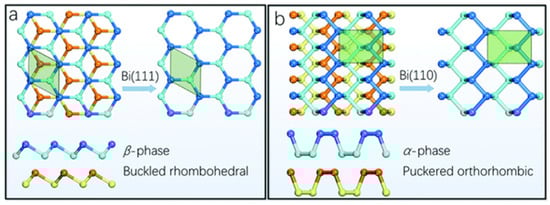
Figure 1.
(a) Top and side views of Bi(111) exhibiting a buckled honeycomb structure, and (b) top and side views of Bi(110) with a puckered black phosphorus-style allotrope. Reprinted with permission from reference [33].
In terms of the mechanical properties, Young’s modulus for 2D pnictogens is regularly higher for the β phase compared to the α counterpart, except for bismuthene, which exhibits the opposite trend [35]. Also, Young’s modulus values decrease as the atomic number increases, i.e., 77.14 N m−2 for phosphorene, above 50.96 N m−2 for arsenene, and >31.44 N m−2 for antimonene, while for bismuthene the same opposite trend is observed, displaying a value of 28.45 N m−2. The shear modulus exhibits the same trend for bismuthene as observed in Young’s modulus.
2.2. Optical Properties
As indicated by computational studies, both α- and β-bismuthene exhibit direct bandgap values, with 0.36 eV for the former and 0.99 eV for the latter. Their absorption coefficients exceed 10−4 cm−1, and their mobility, calculated using the acoustic phonon-limited mobility approach, was estimated to be approximately 10−2 to 10−3 cm2 V−1 s−1, comparable to that reported for black phosphorus [36]. Due to its high atomic weight, bismuth demonstrates a strong spin-orbit coupling (SOC) effect, which is advantageous for spintronic applications as it generates spin-polarized electrons without requiring a strong magnetic field [31]. SOC arises from the interaction between an electron spin and its orbital motion around the nucleus, creating an internal magnetic field that causes energy level splitting [37]. This effect can indirectly control electron spin. Rashba coupling, a type of SOC, enables the control of spin states without a magnetic field by lifting spin degeneracy through structural inversion asymmetry [33]. The SOC effect intensifies with increasing atomic number, making it particularly strong in bismuthene, thereby influencing the bandgap values predicted by theoretical calculations [38]. Aktürk et al. [8] reported a direct bandgap of approximately 0.55 eV for β-bismuthene at the Perdew–Burke–Ernzerhof (PBE) level without considering SOC. However, when SOC was included, an indirect bandgap of approximately 0.51 eV was observed due to Rashba-type splitting in the degenerate bands at the top of the valence band. At the HSE06 level of theory, a direct bandgap between 0.80 eV and 0.99 eV was predicted for single-layered β-bismuthene without SOC, while a bandgap of approximately 0.32 eV was calculated when SOC was considered [33]. Other studies have reported a transition from indirect to direct bandgap and from semiconducting to semi-metallic behavior for β-bismuthene, attributed to biaxial strain or the quantum size effect resulting from decreased thickness [8,18,32].
2.3. Chemical Properties and Gas Adsorption Capabilities of Bismuthene
Regarding chemical properties, the unpaired electrons in bismuthene are highly accessible, similar to that observed for arsenene and antimonene, making it suitable for interacting with various gases, particularly nitrogen-containing ones, like NH3, NO, and NO2. This interaction occurs through the formation of a solid metal-nitrogen covalent bond. The bismuthene sp3 hybridization, along with its buckled configuration, provides it with a strong capacity to adsorb gas molecules. The adsorption ability of specific environmental gas molecules (CO, H2, NO, and NO2) is given by the adsorption energy (Ea) of the gases, which is estimated at −0.77 eV for CO on buckled bismuthene [39]. For H2, the Ea value on bismuthene is 0.008 eV, about five times lower than that for InSe, arsenene, and antimonene. The Ea values for NO and NO2 are −0.33 eV and −0.99 eV, respectively, indicating relatively strong interactions of these gases with bismuthene. These differences in Ea values are attributed to the type of interaction with bismuthene (normal to the surface for CO, tilted configuration for H-H bonds and NO2, and close to the center of the hexagon for NO) and the distance of the gas molecules from the bismuthene surface [39,40]. In this context, some research groups have explored the capacity of folded bismuthene (nanotube-like) for detecting V-series nerve agents, which are highly toxic organophosphorus compounds used as chemical warfare agents. The estimated Ea values for different V-series nerve agents on bismuthene vary from −0.350 eV to −0.673 eV. The interaction between these poisonous agents and the bismuthene surface is crucial for developing bismuthene-based chemical resistive detectors [41].
2.4. Other Properties
Regarding the thermodynamic properties of 2D bismuthene, the calculated phonon spectra for both α- and β-bismuthene do not show imaginary phonon modes, indicating good dynamic stability [6]. Theoretical calculations have suggested that free-standing bismuthene remains stable above room temperature. However, at elevated temperatures (T = 700 K), ab initio calculations reveal that bismuthene loses its dynamic stability [8]. In terms of air stability, 2D black phosphorus rapidly degrades under ambient conditions, making it less suitable for real-world applications. In contrast, bismuthene has demonstrated high environmental stability. Raman analysis has confirmed that bismuthene maintains its structural integrity even after more than one month of exposure to ambient conditions [42]. Theoretical studies also indicate that bismuthene could exhibit 2D topological insulator properties with non-trivial topological edge states, enhancing its potential due to the negligible effect of nonmagnetic backscattering. Additionally, 2D bismuthene exhibits significant nonlinear optical properties, making it suitable for applications in broadband photodetectors, nonlinear optical switching, and phase modulators [31]. The charge carrier mobility of bismuthene is notable, with single crystalline bulk Bi achieving 5.7 × 106 cm2 V⁻1 s⁻1 and thin film Bi reaching 2 × 104 cm2 V⁻1 s⁻1, which is promising for logic transistors. The small effective carrier mass and large mean free path of Bi crystal contribute to its magnetoresistance effect [31].
Lastly, for materials intended for commercial applications, it is essential that they are safe for human health, exhibiting no toxicity, mutagenic, or carcinogenic properties. Current investigations on the cytotoxicity of 2D bismuthene are promising. Studies report that thin layers of bismuthene show negligible cytotoxicity in tests using specific human cells. Additionally, 2D bismuthene exhibits significantly lower toxicity compared to bismuth(III) oxide salts [33].
Given the outstanding properties of 2D bismuthene, controlling its structural, electronic, and physicochemical characteristics is crucial for its implementation in various applications. Effective synthesis methodologies are key strategies for achieving desirable properties. Approaches such as doping, substrate engineering, and chemical or mechanical modifications can tailor these properties to specific uses.
3. Synthesis Routes to Obtain 2D Bismuthene
2D bismuthene can be synthesized using either bottom-up or top-down approaches. The former generally involves chemical conversion methods to transform elemental units (ions, atoms, molecules, etc.) into nanosheets. Common techniques for this approach include pulsed laser deposition (PLD), chemical vapor deposition (CVD), molecular beam epitaxy (MBE), and electron beam (e-beam) evaporation [11]. Conversely, the top-down approach relies on mechanical force or molecular interaction to exfoliate bulk materials, exploiting the weak van der Waals interactions between layers. Methods for the top-down approach include liquid-phase exfoliation, chemical exfoliation, mechanical exfoliation, and etching [11,13,43].
3.1. Bottom-Up Approaches
3.1.1. Chemical Vapor Deposition (CVD)
CVD is a widely used method for producing thin films for their implementation as conductive oxides, passivation layers, dielectrics, and heat-resistant coatings for photovoltaic and microelectronic applications. In this process, a solid material (thin film, powder, or single crystal) is deposited from a vapor generated by a chemical reaction occurring on or near a heated substrate. The final properties of the material can be influenced by varying parameters such as temperature, gas mixture, gas flow rate, and reaction time, among others [44]. In terms of the 2D bismuthene materials, Zhou et al. [45] reported the successful production of 2D bismuth films using the CVD method. The films were grown on both rigid (SiO2/Si) and flexible polyimide substrates, with bismuth powder serving as the precursor material. Similarly, Hu et al. [46] synthesized bismuthene nanoflakes on a Cu foil substrate. The obtained 2D materials exhibited high thermal stability after annealing at 500 °C for 10 min, making them favorable for electrochemical CO2 reduction.
3.1.2. Physical Vapor Deposition (PVD)
PVD is a method used to deposit thin films, differing from CVD in its approach. Pulsed laser deposition (PLD) is a PVD technique where a high-power density pulsed laser beam strikes the target material, causing it to be ejected as a plasma plume and deposited onto a substrate. The PLD process is conducted under high vacuum conditions [47]. This method offers a significant advantage in that the deposited film maintains stoichiometry similar to the target material [48]. Yang et al. [31] successfully achieved high-crystallinity centimeter-scale bismuth layers with uniform surfaces using PLD. The authors obtained 2D Bi(111) and Bi(110) materials at low temperatures (below 100 °C), with thickness controlled by the number of laser pulses. The transport properties of the PLD-grown Bi(111) films were evaluated using back-gate field-effect transistors (FETs) based on few-layer Bi on Si wafer substrates capped with a 300 nm thick SiO2 layer. The thin bismuth layer acted as a gate dielectric insulator and prevented interference from the Si during transport measurements, making it suitable for high-performance electronic devices.
3.1.3. Molecular Beam Epitaxy (MBE)
MBE is a highly suitable methodology for obtaining large-scale, high-quality 2D films with consistent thickness. In this process, materials grow under ultra-high vacuum conditions on a heated crystalline substrate through the interaction of adsorbed species supplied by atomic or molecular beams [49]. The resulting films exhibit the same crystalline structure as the substrate or a structure with similar symmetry, with the lattice parameter differing from the substrate by no more than 10% [44]. The electronic properties and film growth of MBE-deposited thin films are substrate-dependent due to the interaction between the substrate and the 2D structures. For 2D bismuthene thin films, comprehensive studies have been conducted on various substrates, including SiC, Au, graphene, Si, Bi2Te3, and highly oriented pyrolytic graphite (HOPG) [45].
3.1.4. Electron-Beam Epitaxy
The electron-beam epitaxy method, similar to PLD, is an evaporation technique that uses a focused electron beam to deposit ultrathin films on different substrates. The precisely positioned beam heats only a small portion of the target material, minimizing contamination. Jankowski et al. [50] reported the controllable growth of ultrathin bismuthene films (4–20 nm) over an α-Al2O3(0001) insulating substrate. A post-annealing process at 400–450 K revealed a competitive orientation growth between Bi(111) and Bi(110). The production of 2D bismuthene materials through this method is highly beneficial for nanoelectronics applications [51].
3.2. Top-Down Approaches
3.2.1. Liquid Exfoliation
Since the layers of bulk bismuth are held together by van der Waals forces, suitable exfoliation processes can be used to obtain 2D bismuthene with high yields. Liquid exfoliation is a highly efficient and low-cost method that produces high-quality 2D bismuthene materials. In a typical liquid exfoliation process, the strong interaction between bulk Bi and a suitable solvent (such as isopropanol or ethanol, among others) leads to the dispersion of Bi nanosheets after sonication (Figure 2). The solvent choice is crucial for the efficient production of 2D bismuthene [13]. An ideal solvent should effectively exfoliate the material at the highest concentration possible and stabilize the exfoliated 2D materials for extended periods [20]. Ozer et al. [24] reported the synthesis of few-layer 2D bismuthene nanosheets via exfoliation of bulk Bi by incorporating a surfactant-assisted chemical reduction of BiCl3. As the first step, BiCl3 solution was reduced with a borane-tert-butylamine complex in oleyl amine at 120 °C. The resulting precipitate was exfoliated in various solvents using an ultrasonic probe homogenizer. SEM and TEM micrographs confirmed the formation of ultrathin flake-like 2D bismuthene structures. These nanosheets were used as a photoredox catalyst for the C-H arylation of (hetero)arenes with diazonium salts. Additionally, ultrathin bismuth nanosheets are useful in electrocatalytic CO2 reduction reactions to obtain valuable chemicals and sunlight-based fuels [19].
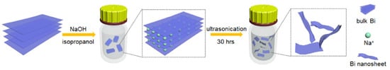
Figure 2.
Schematic illustration of the scalable preparation of ultrathin Bi nanosheets via a liquid-phase exfoliation process. Reprinted with permission from reference [19].
3.2.2. Mechanical Exfoliation
Mechanical exfoliation is a straightforward technique for obtaining 2D bismuthene. In this method, the overlapping layers of bulk bismuth are separated into single or multiple layers using the adhesive force of a tape [43]. To effectively obtain thin Bi layers, the bulk material must exhibit good quality and weak van der Waals forces, ensuring that the resulting layers retain similar properties to the bulk material. However, this technique is limited by the lack of control over the size and morphology of the resulting samples [52].
3.2.3. Electrochemical Exfoliation
Electrochemical exfoliation is a fast and efficient technique that requires moderate fabrication conditions to synthesize 2D bismuthene with high yield. In a typical electrochemical exfoliation process, bulk Bi serves as the cathode and Pt as the anode, both immersed in an appropriate organic solution. This solution is subjected to a direct current (DC) voltage, which helps to increase the interlayer spacing by inserting cations between the molecular layers. Precise control of the DC voltage results in the production of 2D bismuthene with good crystallinity at high yield (Figure 3). Nevertheless, the generation of organic solvent residues can limit the quality of the product [29].
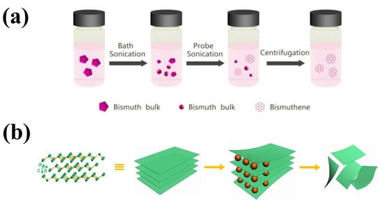
Figure 3.
(a) Schematic of the preparation process of bismuthene via liquid exfoliation (Reprinted with permission from reference [53]) and (b) schematic of a DC voltage exfoliation of 2D bismuthene (Reprinted with permission from reference [54]).
In a recent study, Basyouni et al. [55] reported an electrochemical approach to exfoliate only a few bismuth layers. The authors used a Bi needle as the working electrode partially submerged in an aqueous electrolyte of 0.2 M Na2SO4, with Pt as the counter electrode and Ag/AgCl as the reference electrode (Figure 4). The obtained bismuth material, consisting of 25 atomic layers, showed promising potential for broadband and ultrafast optical limiters that protect against visible-infrared ultrashort pulse laser damage.
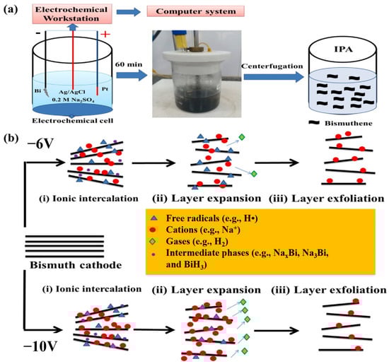
Figure 4.
(a) Fabrication process of bismuthene and (b) mechanism of electrochemically cathodic exfoliation of bismuthene using different voltages. Reprinted with permission from reference [55].
When considering liquid-based exfoliation methods, the physical and chemical properties of 2D bismuthene can be influenced by the solvents used, the duration of ultrasonic treatment, and the centrifugal rate. An advantage of these methods, such as liquid exfoliation, is the wide range of solvents that can be used, including N-methyl 2-pyrrolidone (NMP), dimethylformamide (DMF), dimethyl sulfoxide (DMSO), sulfuric acid, isopropanol (IPA), acetone, water, and ethanol. The main effects of using different solvents on the synthesis and characteristics of the obtained materials are listed below:
- A specific solvent should demonstrate vast differences in peeling efficiency compared to the original procedure, stabilize the obtained nanosheets, and prevent gathering.
- Using different solvents may modify the physical and chemical characteristics of nanosheets [56].
- Methodologies assisted with ultrasonic treatment can improve the interaction between solvent and precursors as the energy provided helps weaken van der Waals forces between the 2D bismuthene layers [5].
- An adequate interaction between solvent and the bismuthene surface can lead to a stable dispersion of the obtained 2D materials [5,11]. Furthermore, the exfoliation process can be optimized when the tension in the solvent surface is comparable to that of bismuthene [57].
From the application perspective, selecting a suitable solvent in liquid exfoliation to obtain bismuthene is crucial for the process efficiency and the final properties of the resulting material. Some authors report the use of different solvents in liquid exfoliation. Li et al., for instance, prepared borophene using liquid exfoliation with two different solvents (DMF and IPA), and varying the centrifugal rate to modify the material thickness and size. The resulting thickness with DMF was 1.8 nm (4 borophene layers), whereas for IPA the material thickness was higher (4.7 nm or 11 borophene layers) [57].
Table 1 summarizes the techniques employed in elaborating 2D bismuthene and their main features.

Table 1.
Examples of bismuthene synthesis routes and obtained dimensions.
In conclusion, there are many methods for preparing 2D-Xenes materials. However, the choice of the optimal method to synthesize 2D bismuthene depends on several requirements, such as the properties of the material for a particular application, cost-effectiveness, and scalability of the process. The methodologies for preparing bismuthene present some advantages and drawbacks, which can limit their applicability, as summarized in Table 2. For that reason, some strategies have been proposed to overcome the main challenges for each method, such as the combination of different processes, innovative approaches, and the development of new techniques. This information could be used as a guide for synthesizing high-quality 2D bismuthene for its use in high-performance devices.
Table 2.
Advantages and disadvantages of different bismuthene synthesis methodologies.
4. Photocatalytic Activity of 2D Bismuthene and Bismuthene-Derived Materials
Climate change is a global concern linked to the continuous release of CO2 into the atmosphere due to the current humankind dependence on fossil fuels. Despite significant efforts by the scientific community to reduce regional and global CO2 emissions, practical solutions remain elusive. CO2 removal methods include pre- and post-combustion CO2 capture via physical or chemical solvent scrubbing, membranes and adsorbents, and geological sequestration. However, these processes are highly energy-intensive and thus expensive [58]. Photocatalysis emerges as a promising, practical, and cost-effective approach for CO2 and nitrogen reduction reactions (CO2RR and NRR, respectively), hydrogen evolution reactions, and other photoactivated processes [59].
Photocatalysis accelerates chemical reactions through semiconducting materials under light irradiation, requiring minimal energy input at low operating costs, and can be performed under ambient conditions. Upon the light absorption by the semiconductor, free electrons migrate from the valence band (VB) to the conduction band (CB), forming the hole-electron pairs [60]. These photogenerated charge carriers migrate to the photocatalyst surface and react with species in the surrounding medium, including water and oxygen molecules, leading to redox reactions. However, not all photogenerated pairs participate in surface reactions, as some recombine through radiative and non-radiative routes. To reduce the charge carrier recombination rate and increase the photocatalysis performance, strategies such as band gap tuning, morphology control, surface defect engineering, co-catalyst utilization, and heterojunction construction have been explored to enhance photocatalytic efficiency [58]. The emergence of 2D materials with sheet-like structures and thicknesses of a few atomic layers has arisen as a potential strategy to meet these challenges [3]. When 2D materials are thinned to their physical limits, they exhibit novel properties that differ from their bulk counterparts. For example, larger surface-to-volume ratios provide more active surface sites. The atomic thickness minimizes the distance that charge carriers must travel from the bulk to the material surface, reducing the charge carrier recombination rate. Additionally, the light absorption capacity can be adjusted by tuning the number of layers [11,61]. Recent studies have shown that forming an intimate interface with a co-catalyst (heterojunction) produces a synergistic effect, optimizing light absorption and charge transfer while maintaining the spatial separation of photogenerated carriers [62].
Figure 5 illustrates the various applications of 2D materials in heterogeneous photocatalysts for environmental purposes.
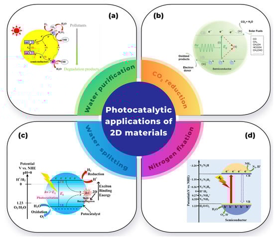
Figure 5.
Photocatalytic applications of 2D materials in: (a) water purification (Adapted with permission from reference [11]), (b) CO2 reduction reaction (Adapted with permission from reference [63]), (c) water-splitting reaction (Adapted with permission from reference [64]), and (d) nitrogen reduction reaction (Adapted with permission from reference [65]).
4.1. Photocatalytic Activity of Bismuthene-Based Materials for CO2 Reduction Reaction
Since the early work of Halman on CO2 reduction for producing solar fuels [66], photocatalytic-based strategies have garnered significant interest due to their effectiveness and eco-friendly features [19,67]. Key research areas include optimizing light absorption and enhancing the separation and mobility of photoinduced charge carriers to address the low conversion efficiencies associated with the wide bandgap value of common photocatalyst materials, including TiO2, ZnO, and ZnS, as well as reducing the recombination of photogenerated carriers.
While many studies using ultrathin 2D materials for CO2 reduction have employed electrocatalytic approaches, an increase in photocatalytic schemes has been observed in recent years. Current research on photocatalytic strategies focuses on two main aspects: (1) the formation of 2D/2D interfaces, and (2) the inclusion of ultrathin 2D materials. Addressing the persistent limitations of photocatalysis involves properly integrating these two aspects. Including 2D materials in the photocatalytic process increases the reactive surface area, enhancing the conversion rate of the CO2 reduction reaction. This property is further amplified by ultrathin films, which offer a higher concentration of active sites due to their reduced thickness. Additionally, 2D/2D heterostructures improve effective electron-hole separation and charge transfer processes [64].
In the CO2 reduction reaction, photogenerated electrons are involved in recation pathways that yield products like CO, CH4, formic acid, formaldehyde, and methanol. As can be seen in Equations 1 to 6 (potentials vs. NHE electrode at pH 7 [68,69]), CO and formic acid (HCO2H) are efficiently generated, as their formation requires only two electrons, while the CH4 formation requires eight electrons [68]. Among these products, CH4, with an enthalpy of combustion of −890.03 kJ mol−1, can store the most solar energy as chemical energy [70], making this a product of economic interest. Still, the CO2 reduction into CH4 is hindered by the high number of photoelectrons that need to be transferred, making the reaction mechanistically complex and slow. Advanced photocatalysts are required to direct the selectivity of CO2 photoreduction toward desired products.
The inclusion of 2D bismuthene in 2D/2D heterostructures facilitates the transfer of photogenerated electrons to the photocatalyst surface, increasing the number of electrons involved in the CO2 conversion [71], and thus the potential formation of desired products CH4 and formic acid. When 2D bismuthene was coupled with bismuth molybdate (Bi/BMo) and bismuth molybdate modified with oxygen vacancies (Vo) (Bi/BMo-Vo) (Figure 6a,b), a photocatalyst composite with tunable interfacial charge transfer features was achieved by varying the Vo concentration. Electrostatic attraction between semiconductors generated an Ohmic contact interface with low charge transfer resistance, inhibiting charge recombination, while oxygen vacancies significantly enhanced the visible light absorption ability of the photocatalyst and acted as traps for photogenerated electrons, which were attracted to the defect energy levels. All this resulted in high CO2 reduction, although low selectivity toward CH4 formation was observed [72]. The loading of 2D bismuthene can also impact the photocatalytic performance of 2D/2D composite materials. For instance, in a Cs2AgBiBr6 perovskite/bismuthene photocatalyst (Figure 6c,d), an optimal bismuthene loading of 1 wt.% improved the selectivity of the photocatalyst toward CO2 transformation into CH4 [27]. Effective charge separation and the suppression of electron-hole recombination due to good interfacial contact between the perovskite and 2D bismuthene were responsible for the enhanced photocatalytic activity and selectivity.
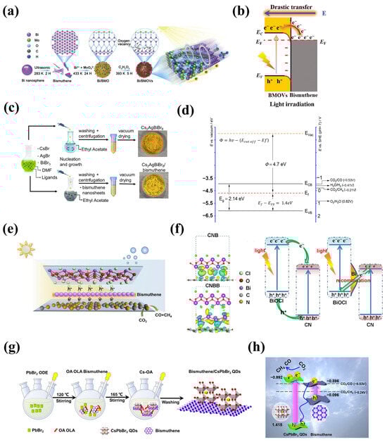
Figure 6.
Synthesis and band structure alignment of bismuthene-based photocatalyst for CO2 reduction reaction: (a,b) Bi/BMoVo (Adapted with permission from reference [72]), (c,d) Cs2AgBiBr6/bismuthene (Adapted with permission from reference [27]), (e,f) C3N4/bismuthene/BiOCl (Adapted with permission from reference [73]), and (g,h) bismuthene/CsPbBr3 quantum dots (Adapted with permission from reference [67]).
Constructing classic Z-scheme or S-scheme semiconductor systems is a widely investigated strategy in photocatalysis. Zhang et al. [73] proposed a modified 2D/2D/2D Z-scheme consisting of C3N4/bismuthene/BiOCl, where bismuthene nanosheets served as electron mediators, increasing charge conductivity, providing abundant metal-semiconductor contact sites, and shortening the charge diffusion distance of photogenerated charge carriers (Figure 6e,f). This configuration benefited the photocatalytic CO2 reduction reaction and improved the stability of the catalyst across several reaction cycles [64,74]. On the other hand, the S-scheme material bismuthene/CsPbBr3 quantum dots (Figure 6g,h) [67] was able to photocatalytically reduce CO2 without using any sacrificial agent (e.g., methanol or isopropanol), which translates to a greener reaction system. This S-scheme composite exhibited the highest CH4 yields compared to individual photocatalysts under UV-visible light irradiation, with a selectivity of around 84%. The stability of the photocatalyst was maintained after three consecutive reaction cycles, showing no significant reduction in efficiency.
Table 3 summarizes the currently published works on photocatalytic CO2 reduction reactions using bismuthene-based materials, highlighting the selectivity toward CH4 production.
Table 3.
Photocatalytic performance of bismuthene-based materials in the CO2 reduction reaction.
The use of 2D bismuthene has also been reported for the electroreduction of CO2 since the early 2020s. For example, Yang et al. [79] reported the first study on the application of bismuthene for the efficient electroreduction of CO2 to formate, showing a faradaic efficiency of 99% at −580 mV vs. reversible hydrogen electrode, and stability for up to 75 h. Subsequent studies have shown that the presence of stable Bi-O bonds can increase the adsorption efficiency of CO2 on the surface of bismuthene, improving the conversion efficiency to formate [80]. In a more recent work, the growth of bismuthene nanoflakes on Cu(111) foil covered by an h-BN layer resulted in a material stable at high temperatures (500 °C) with high faradaic efficiencies (over 96%) for the production of formate through the electroreduction of CO2 [81]. Future studies are underway to obtain valuable products from the electrocatalytic reduction of CO2 using 2D bismuthine-based materials.
4.2. Photocatalytic Activity for Degradation of Organic Pollutants
Over the past three decades, heterogeneous photocatalysis has emerged as a promising method for removing organic pollutants from water [82]. Due to its activation method and mode of action, the photocatalytic process is feasible only as a polishing step in the treatment of wastewater and drinking water. Moreover, space and energy requirements have hindered the scalability of this technology in real-world conditions [83]. One approach to enhance the scalability of heterogeneous photocatalysis is to develop catalyst materials that are active under visible light irradiation, exhibit high conversion rates, are easy to recover, and demonstrate high reusability. These catalysts must efficiently oxidize organic pollutants to their mineral components, primarily CO2 and H2O, to prevent the formation of hazardous intermediates that pose more significant risks to exposed organisms compared to the parent compounds. Emerging contaminants, such as pharmaceuticals and plasticizers, present challenges due to their low removal rates in conventional water treatment systems, posing risks to ecosystems and human health due to their high and diverse bioactivity [84,85]. Heterogeneous photocatalysis, with its exhaustive and non-selective oxidation, can offer a potential solution to mitigate these environmental risks. Commonly used photocatalysts like TiO2 and ZnO are mainly activated under UV light irradiation, and their exhausted forms can be hazardous to terrestrial and aquatic organisms [86,87]. This has driven extensive research into finding more efficient and sustainable alternatives. For example, various bismuth-based semiconductors have been synthesized using eco-friendly methods to achieve competitive removal rates of emerging contaminants under visible light irradiation [88]. Materials such as bismuth oxide, bismuth sulfide, and ternary bismuth compounds show promise for larger-scale application in real-world water treatment systems [88,89,90]. In particular, 2D bismuthene materials could enhance photocatalytic efficiency of semiconductor-semiconductor heterostructure materials by facilitating the separation of charge carriers, thus improving the conversion of oxidation and reduction reactions on the catalyst surface. This potential has been harnessed in the CO2 reduction reaction process, while there are no studies to date using 2D bismuthene materials for the photocatalytic degradation of organic pollutants in water under visible light irradiation, presenting a compelling direction for future research (see Table 4).
In this context, 2D bismuth-containing complex oxides, including bismuth subcarbonate (Bi2O2CO3), have been investigated for their ability to degrade organic contaminants under visible light irradiation [91]. Ultrathin sheets of Bi2O2CO3 can be obtained when electrochemically exfoliated bismuthene nanosheets are naturally exposed to air at room temperature (Figure 7). Compared to its nanoparticulate counterparts, obtained via hydrothermal methods, Bi2O2CO3 nanosheets exhibited exceptional textural parameters, including a much larger surface area and pore volume. Additionally, optical characterization showed a broadened light absorption range and low recombination rates. This material demonstrated superior performance in the degradation of ciprofloxacin due to the generation of reactive oxygen species, such as hydroxyl radicals, which is uncommon for bismuth-based materials.
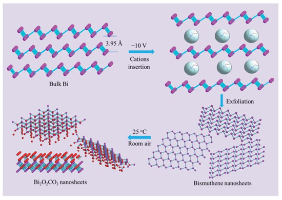
Figure 7.
Schematic representation of the synthesis of Bi2O2CO3 from bismuthene nanosheets. Rerpineted with permission from reference [91].
4.3. Other Photocatalytic Applications of Bismuthene-Based Materials
Photocatalytic H2 generation through water splitting is an eco-friendly process to generate renewable energy, with low production of greenhouse gases, as water is the only byproduct of H2 combustion [92]. To achieve the efficient reduction of water molecules via photocatalysis, catalysts must possess, in addition to the appropriate morphological and textural properties (i.e., small particle size, high surface area, and crystallinity, among others), a high potential of photoelectrons in the conduction band to carry out the reduction of H+ to H2 [93]. At the same time, it is necessary to prevent photo-holes from reoxidizing the produced H2 by using appropriate sacrificial agents. To date, only a few photocatalysts can achieve overall water splitting with a stoichiometric H2 and O2 evolution (2:1 molar ratio). However, these potential candidates are typically active only under UV light irradiation [94,95]. To overcome the limitations of conventional photocatalysts, ultrathin 2D semiconductor-based materials are considered promising alternatives for the direct transformation of water into H2 through the water-splitting process [96,97], although practical implementation in the field is still in its infancy. Ab initio molecular dynamics have provided insights into a 2D InTe/bismuthene Z-scheme photocatalyst [98], analyzing several configurations to identify the stacking method with the highest solar-to-hydrogen (STH) conversion efficiency. Results show that all configurations adhere to the photocatalytic hydrogen evolution reaction (HER) and oxygen evolution reaction (OER) standards. The formation of a built-in electric field between the inner surfaces of the heterostructure supports the Z-scheme formation, with a maximum STH of 9.67%.
Photocatalytic reduction of N2 offers an alternative to the industrial Haber–Bosch process, which relies heavily on the use of fossil fuels. This process involves N2 molecules capturing photoexcited electrons and protons from a reactant to generate NH3, with hole sacrificial agents (EDTA, methanol, ethanol, etc.) used to prevent hole accumulation and photocatalyst corrosion [99]. Overall nitrogen reduction reaction (E° vs. NHE) comprises two coupled redox half-reactions triggered by six electrons, six protons, and six holes (Equations (7) and (8)).
The primary obstacle to the N2 reduction process in aqueous solution is the high N≡N dissociation energy of 941 kJ mol−1 [59]. In this context, several 2D and 2D/2D photocatalysts (such as Cu2O/BN and MnO2/g-C3N4) have been successfully implemented in photocatalytic nitrogen fixation to ammonia, while the use of ultrathin 2D bismuthene or bismuthene-containing photocatalysts has so far been limited to electrocatalytic approaches. As indicated by Li et al. [98], layered bismuth and bismuth oxyhalide photocatalysts, including 2D thin bismuth-layered materials, have significant potential for high NH3-yield photocatalytic nitrogen fixation. Therefore, future studies should focus on the implementation of bismuthene-based materials in the photocatalytic nitrogen reduction reactions by harnessing the low bandgap and high electric conductivity of this kind of 2D material.
Table 4.
Photocatalytic and non-photocatalytic applications of performance of bismuthene-based materials.
Table 4.
Photocatalytic and non-photocatalytic applications of performance of bismuthene-based materials.
| Application | Production Method | Bismuthene Characteristics | Performance | Ref. |
|---|---|---|---|---|
| Photocatalytic degradation of pollutants | ||||
| Photocatalytic removal of nitrogen oxide (NO) | Synthesis in aqueous solution | Bi lateral size 100–200 nm | 42% removal was achieved using Bi nanomaterial under 280 nm light irradiation (compared to 6% efficiency under dark conditions) | [57] |
| Other photocatalytic applications of bismuthene-based materials | ||||
| Photoredox catalyst in C-H arylation of (hetero)arenes | Ultrasonic exfoliation of bulk bismuth powder | 550 nm lateral and 5 nm thick, smoothed surface and XRD peaks associated with bulk Bi | High catalytic activity in the C–H arylation of heteroarenes such as furan, thiophene, pyrrole, and benzene with aryl diazonium salts under indoor light illumination | [100] |
| Boosting CO2 Hydrogenation Reduction | Aqueous-based reflux method | Bi-sheets of 1.2–1.5 nm thick (2–3 monolayers). No signals associated with bismuth oxide were found | Ratios of photogenerated electron for reduction of CO2 to CO and CH4 for bismuthene were 58.24 and 300.5 times higher than those of bulk Bi, respectively | [101] |
| Non-photocatalytic applications | ||||
| Oxygen reduction reaction (ORR) | Mechanical grinding assisted by ionic liquid | Sheet size: 20 nm lateral size and 5 nm thick | High current density (2.39 mA) at 0.17 VRHE in linear sweep voltammetry, indicating high photoactivity towards ORR | [102] |
Lastly, it is crucial to understand the stability of 2D bismuthene materials so they can be massively synthesized, stored, implemented in photocatalytic procedures, and further upscaled. In photocatalytic schemes, the agents that can lead to the degradation of the catalyst are light, dissolved oxygen, and water molecules. Kistanov et al. [103] explored the stability of 2D pnictogens under environmental conditions through a first-principles investigation, finding bismuthene and antimonene to be the most stable members of this group. DFT-based calculations predicted a strong energy adsorption (Ea) of the O2 molecule on the bismuthene surface (Ea = −0.61 eV), in contrast to a lower interaction with the water molecule (Ea = −0.14 eV). Moreover, a low energy barrier for the dissociation of the O2 molecule (Eb = 0.6 eV) indicated rapid oxidation of the bismuthene surface. Recent studies [24] have evaluated the stability of α- and β-bismuthene under environmental conditions, finding no generation of Bi2O3 through X-ray diffraction analysis, which contrasts with theoretical studies indicating the possible formation of mild oxidized bismuthene upon contact with O2 molecules. It is possible that such oxidized species are unable to be determined through X-ray diffraction, although theoretical and experimental studies are needed on this topic. According to Kistanov et al. [103], superficially oxidized bismuthene maintains structural stability because the terminated O atom in the apical Bi-O group traps water molecules and prevents their dissociation, thereby hindering the formation of acidic species that are known to lead to the degradation of phosphorene, arsenene, and even InSe. The key to the environmental stability of bismuthene may lie in the behavior of adsorbed water molecules, as well as in the intrinsic and chemical properties of bismuth, including atomic number and electronegativity, respectively.
5. Summary and Prospects
The recent advancements in 2D metallene materials have attracted the researchers’ attention due to their unique properties and broad potential for various applications. In particular, 2D bismuthene, with its atomically thin and layered structure, offers advantages over its bulk form, including a layer-dependent optical bandgap, high charge carrier mobility, and stability. These features make it an excellent candidate for use in electronics and photocatalysis. This review has highlighted the recent progress in environmental photocatalysis applications of 2D bismuthene-based materials, discussing their crystalline and electronic structures. Both top-down and bottom-up synthesis methods were examined, emphasizing the importance of producing large-area materials for practical applications. Current scalable growth methods for 2D bismuthene, such as CVD, PLD, and MBE, face challenges, including poor controllability, slow growth rates, and high costs, which hinder commercialization. Hence, developing a direct synthesis method for high-quality 2D bismuthene films is essential. Additionally, incorporating green chemistry principles into the synthesis process is crucial from a life-cycle analysis perspective, especially for environmental photocatalysis applications. Reducing the use of hazardous precursors, solvents, and additives, along with designing low-energy intensive synthesis paths, are the first steps toward a greener synthesis of 2D materials, which have demonstrated biocompatibility and overall safer chemical profiles.
One significant challenge in implementing 2D bismuthene in heterogeneous photocatalysis is its oxidation into amorphous bismuth oxide due to its thinness and semimetal nature, which reduces its photocatalytic efficiency. Integrating 2D bismuthene photocatalysts into a photoelectrochemical system could prevent oxidation, although experimental studies are necessary. The weak interlayer interactions in 2D bismuthene enable the formation of heterostructures with other 2D materials or materials of different dimensions, significantly enhancing their properties, stability and applications. The tunable band alignment and combined advantages of diverse materials make 2D bismuthene heterostructures promising for high-performance photocatalytic applications. Furthermore, the large contact surface and highly exposed surface atoms in these heterostructures might create a substantial internal electric field, boosting catalytic conversion rates. Therefore, it is highly encouraged to continue exploring the photonic and photocatalytic applications of 2D bismuthene heterostructures.
Author Contributions
Conceptualization, J.C.D.-Á.; investigation, A.S.-L., K.P.-C. and A.R.-S.; writing—original draft preparation, J.C.D.-Á., A.S.-L. and K.P.-C.; writing—review and editing, R.Z.; funding acquisition, J.C.D.-Á. All authors have read and agreed to the published version of the manuscript.
Funding
This research was funded by Secretaría de Educación, Ciencia, Tecnología e Innovación de la Ciudad de México (SECITI), through the Project with grant number SECITI/047/2016.
Conflicts of Interest
The authors declare no conflicts of interest. The funders had no role in the design of the study; in the collection, analyses, or interpretation of data; in the writing of the manuscript; or in the decision to publish the results.
References
- Baig, N. Two-Dimensional Nanomaterials: A Critical Review of Recent Progress, Properties, Applications, and Future Directions. Compos. Part A Appl. Sci. Manuf. 2023, 165, 107362. [Google Scholar] [CrossRef]
- Patel, N.F.; Bhakhar, S.A.; Jagani, H.S.; Solanki, G.K.; Pataniya, P.M. Synthesis, Characterization and Optoelectronic Application of Bi2Se3 Thin Film Prepared by Thermal Evaporation Technique. Opt. Mater. 2023, 136, 113403. [Google Scholar] [CrossRef]
- Tan, C.; Cao, X.; Wu, X.J.; He, Q.; Yang, J.; Zhang, X.; Chen, J.; Zhao, W.; Han, S.; Nam, G.H.; et al. Recent Advances in Ultrathin Two-Dimensional Nanomaterials. Chem. Rev. 2017, 117, 6225–6331. [Google Scholar] [CrossRef]
- Wu, Z.; Hao, J. Electrical Transport Properties in Group-V Elemental Ultrathin 2D Layers. NPJ 2D Mater. Appl. 2020, 4, 4. [Google Scholar] [CrossRef]
- Wang, B.; Zhong, S.; Ge, Y.; Wang, H.; Luo, X.; Zhang, H. Present Advances and Perspectives of Broadband Photo-Detectors Based on Emerging 2D-Xenes beyond Graphene. Nano Res. 2020, 13, 891–918. [Google Scholar] [CrossRef]
- Zhang, S.; Xie, M.; Li, F.; Yan, Z.; Li, Y.; Kan, E.; Liu, W.; Chen, Z.; Zeng, H. Semiconducting Group 15 Monolayers: A Broad Range of Band Gaps and High Carrier Mobilities. Angew. Chem. Int. Ed. 2016, 55, 1666–1669. [Google Scholar] [CrossRef] [PubMed]
- Patel, N.F.; Bhakhar, S.A.; Gupta, S.U.; Chauhan, B.L.; Solanki, G.K. Influence on Electrical Properties of Pristine Bulk Bi2Se3 Compound by Substitutional Doping of ‘In’. J. Mater. Sci. Mater. Electron. 2023, 34, 124. [Google Scholar] [CrossRef]
- Aktürk, E.; Aktürk, O.Ü.; Ciraci, S. Single and Bilayer Bismuthene: Stability at High Temperature and Mechanical and Electronic Properties. Phys. Rev. B 2016, 94, 014115. [Google Scholar] [CrossRef]
- Freitas, R.R.Q.; Rivelino, R.; De Brito Mota, F.; De Castilho, C.M.C.; Kakanakova-Georgieva, A.; Gueorguiev, G.K. Topological Insulating Phases in Two-Dimensional Bismuth-Containing Single Layers Preserved by Hydrogenation. J. Phys. Chem. C 2015, 119, 23599–23606. [Google Scholar] [CrossRef]
- Pumera, M.; Sofer, Z. 2D Monoelemental Arsenene, Antimonene, and Bismuthene: Beyond Black Phosphorus. Adv. Mater. 2017, 29, 1605299. [Google Scholar] [CrossRef]
- Shwetharani, R.; Kainthla, I.; Dongre, S.S.; D’Souza, L.; Balakrishna, R.G. Recent Advances in Ecofriendly 2D Monoelemental Bismuthene as an Emerging Material for Energy, Catalysis and Biomedical Applications. J. Mater. Chem. C Mater. 2023, 11, 6777–6799. [Google Scholar]
- Sujita, P.; Vadivel, S.; Wacławek, S.; Paul, B. Few Layers of Bismuthene as an Ideal Material for Electrochemical Applications: A Review. Inorg. Chem. Commun. 2024, 167, 112739. [Google Scholar] [CrossRef]
- Li, H.; Yang, Z. Recent Progress in Synthesis and Photonic Applications of Two-Dimensional Bismuthene. Appl. Sci. 2023, 13, 6885. [Google Scholar] [CrossRef]
- Nguyen, D.K.; Bao, T.V.; Kha, N.A.; Ponce-Pérez, R.; Guerrero-Sanchez, J.; Hoat, D.M. Searching for D0 Spintronic Materials: Bismuthene Monolayer Doped with IVA-Group Atoms. RSC Adv. 2023, 13, 5885–5892. [Google Scholar] [CrossRef] [PubMed]
- Kecik, D.; Özçelik, V.O.; Durgun, E.; Ciraci, S. Structure Dependent Optoelectronic Properties of Monolayer Antimonene, Bismuthene and Their Binary Compound. Phys. Chem. Chem. Phys. 2019, 21, 7907–7917. [Google Scholar] [CrossRef] [PubMed]
- Reis, F.; Li, G.; Dudy, L.; Bauernfeind, M.; Glass, S.; Hanke, W.; Thomale, R.; Schäfer, J.; Claessen, R. Bismuthene on a SiC Substrate: A Candidate for a High-Temperature Quantum Spin Hall Material. Science 2017, 357, 287–290. [Google Scholar] [CrossRef] [PubMed]
- Hsu, C.H.; Huang, Z.Q.; Chuang, F.C.; Kuo, C.C.; Liu, Y.T.; Lin, H.; Bansil, A. The Nontrivial Electronic Structure of Bi/Sb Honeycombs on SiC(0001). New J. Phys. 2015, 17, 025005. [Google Scholar] [CrossRef]
- Liu, M.Y.; Huang, Y.; Chen, Q.Y.; Li, Z.Y.; Cao, C.; He, Y. Strain and Electric Field Tunable Electronic Structure of Buckled Bismuthene. RSC Adv. 2017, 7, 39546–39555. [Google Scholar] [CrossRef]
- Zhang, W.; Hu, Y.; Ma, L.; Zhu, G.; Zhao, P.; Xue, X.; Chen, R.; Yang, S.; Ma, J.; Liu, J.; et al. Liquid-Phase Exfoliated Ultrathin Bi Nanosheets: Uncovering the Origins of Enhanced Electrocatalytic CO2 Reduction on Two-Dimensional Metal Nanostructure. Nano Energy 2018, 53, 808–816. [Google Scholar] [CrossRef]
- Shen, J.; He, Y.; Wu, J.; Gao, C.; Keyshar, K.; Zhang, X.; Yang, Y.; Ye, M.; Vajtai, R.; Lou, J.; et al. Liquid Phase Exfoliation of Two-Dimensional Materials by Directly Probing and Matching Surface Tension Components. Nano Lett. 2015, 15, 5449–5454. [Google Scholar] [CrossRef]
- Mourdikoudis, S.; Antonatos, N.; Mazánek, V.; Marek, I.; Sofer, Z. Simple Bottom-up Synthesis of Bismuthene Nanostructures with a Suitable Morphology for Competitive Performance in the Electrocatalytic Nitrogen Reduction Reaction. Inorg. Chem. 2022, 61, 5524–5538. [Google Scholar] [CrossRef] [PubMed]
- Kokabi, A.; Mardanian, R.; Touski, S.B. Electronic and Nonlinear Optics Investigation of Bismuthene Nanosheet as a Promising Photocatalyst. Phys. Solid. State 2023, 65, 156–165. [Google Scholar] [CrossRef]
- Yue, C.; Zhu, L.; Qiu, Y.; Du, Z.; Qiu, J.; Liu, F.; Wang, F. Recent Advances of Plasmonic Elemental Bi Based Photocatalysts in Environmental Remediation and Energy Conversion. J. Clean Prod. 2023, 392, 136017. [Google Scholar] [CrossRef]
- Ozer, M.S.; Eroglu, Z.; Yalin, A.S.; Kılıç, M.; Rothlisberger, U.; Metin, O. Bismuthene as a Versatile Photocatalyst Operating under Variable Conditions for the Photoredox C[Sbnd]H Bond Functionalization. Appl. Catal. B 2022, 304, 120957. [Google Scholar] [CrossRef]
- Qi, M.; Dai, S.; Wu, P. Prediction of Electronic and Magnetic Properties in 3d-Transition-Metal X-Doped Bismuthene (X = V, Cr, Mn and Fe). Appl. Surf. Sci. 2019, 486, 58–64. [Google Scholar] [CrossRef]
- Ge, M.; Yang, C.L.; Wang, M.S.; Ma, X.G. Photocatalytic Hydrogen Generation from Overall Water Splitting with Direct Z-Scheme Driven by Two-Dimensional InTe/Bismuthene Heterostructure. Int. J. Hydrog. Energy 2023, 48, 138–146. [Google Scholar] [CrossRef]
- Sena, M.S.; Cui, J.; Baghdadi, Y.; Rattner, E.; Daboczi, M.; Lopes-Moriyama, A.L.; dos Santos, A.G.; Eslava, S. Lead-Free Halide Perovskite Cs2AgBiBr6/Bismuthene Composites for Improved CH4 Production in Photocatalytic CO2 Reduction. ACS Appl. Energy Mater. 2023, 6, 10193–10204. [Google Scholar] [CrossRef] [PubMed]
- Mannix, A.J.; Kiraly, B.; Hersam, M.C.; Guisinger, N.P. Synthesis and Chemistry of Elemental 2D Materials. Nat. Rev. Chem. 2017, 1, 0014. [Google Scholar] [CrossRef]
- Li, L.; Zhang, D.; Cao, M.; Deng, J.; Ji, X.; Wang, Q. Electrochemical Synthesis of 2D Antimony, Bismuth and Their Compounds. J. Mater. Chem. C Mater. 2020, 8, 9464–9475. [Google Scholar] [CrossRef]
- Lu, Y.; Xu, W.; Zeng, M.; Yao, G.; Shen, L.; Yang, M.; Luo, Z.; Pan, F.; Wu, K.; Das, T.; et al. Topological Properties Determined by Atomic Buckling in Self-Assembled Ultrathin Bi(110). Nano Lett. 2015, 15, 80–87. [Google Scholar] [CrossRef]
- Yang, Z.; Wu, Z.; Lyu, Y.; Hao, J. Centimeter-Scale Growth of Two-Dimensional Layered High-Mobility Bismuth Films by Pulsed Laser Deposition. InfoMat 2019, 1, 98–107. [Google Scholar] [CrossRef]
- Yao, J.D.; Shao, J.M.; Yang, G.W. Ultra-Broadband and High-Responsive Photodetectors Based on Bismuth Film at Room Temperature. Sci. Rep. 2015, 5, 12320. [Google Scholar] [CrossRef] [PubMed]
- Liu, X.; Zhang, S.; Guo, S.; Cai, B.; Yang, S.A.; Shan, F.; Pumera, M.; Zeng, H. Advances of 2D Bismuth in Energy Sciences. Chem. Soc. Rev. 2020, 49, 263–285. [Google Scholar] [CrossRef] [PubMed]
- Kowalczyk, P.J.; Mahapatra, O.; Le Ster, M.; Brown, S.A.; Bian, G.; Wang, X.; Chiang, T.C. Single Atomic Layer Allotrope of Bismuth with Rectangular Symmetry. Phys. Rev. B 2017, 96, 205434. [Google Scholar] [CrossRef]
- Allen, O.J.; Kang, J.; Wang, Y. First-Principles Study of Group VA Monolayer Passivators for Perovskite Solar Cells. ACS Appl. Nano Mater. 2023, 6, 4279–4287. [Google Scholar] [CrossRef]
- Qiao, J.; Kong, X.; Hu, Z.X.; Yang, F.; Ji, W. High-Mobility Transport Anisotropy and Linear Dichroism in Few-Layer Black Phosphorus. Nat. Commun. 2014, 5, 4475. [Google Scholar] [CrossRef]
- Portillo-Cortez, K.; Martínez, A.; Dutt, A.; Santana, G. N719 Derivatives for Application in a Dye-Sensitized Solar Cell (DSSC): A Theoretical Study. J. Phys. Chem. A 2019, 123, 10930–10939. [Google Scholar] [CrossRef] [PubMed]
- Premasiri, K.; Gao, X.P.A. Tuning Spin-Orbit Coupling in 2D Materials for Spintronics: A Topical Review. J. Phys. Condens. Matter 2019, 31, 193001. [Google Scholar] [CrossRef] [PubMed]
- Pan, W.; Qi, N.; Zhao, B.; Chang, S.; Ye, S.; Chen, Z. Gas Sensing Properties of Buckled Bismuthene Predicted by First-Principles Calculations. Phys. Chem. Chem. Phys. 2019, 21, 11455–11463. [Google Scholar] [CrossRef]
- Khadiullin, S.; Davletshin, A.; Zhou, K.; Korznikova, E. TMS 2020 149th Annual Meeting & Exhibition Supplemental Proceedings; Springer: Cham, Switzerland, 2020; ISBN 978-3-030-36295-9. [Google Scholar]
- Bhuvaneswari, R.; Maria, J.P.; Nagarajan, V.; Chandiramouli, R. DFT Study on the Interaction Properties of V-Series Nerve Agent Molecules on Novel Bismuthene Nanotubes. J. Inorg. Organomet. Polym. Mater. 2019, 29, 2226–2236. [Google Scholar] [CrossRef]
- Lu, L.; Liang, Z.; Wu, L.; Chen, Y.X.; Song, Y.; Dhanabalan, S.C.; Ponraj, J.S.; Dong, B.; Xiang, Y.; Xing, F.; et al. Few-Layer Bismuthene: Sonochemical Exfoliation, Nonlinear Optics and Applications for Ultrafast Photonics with Enhanced Stability. Laser Photon Rev. 2018, 12, 1700221. [Google Scholar] [CrossRef]
- Gao, P.; Xiao, Y.; Wang, Y.; Li, L.; Li, W.; Tao, W. Biomedical Applications of 2D Monoelemental Materials Formed by Group VA and VIA: A Concise Review. J. Nanobiotechnol. 2021, 19, 96. [Google Scholar] [CrossRef] [PubMed]
- Carlsson, J.-O.; Martin, P.M. Chemical vapor deposition. In Handbook of Deposition Technologies for Films and Coatings; Martin, P.M., Ed.; Elsevier: Amsterdam, The Netherlands, 2009; pp. 314–363. [Google Scholar]
- Zhou, Q.; Lu, D.; Tang, H.; Luo, S.; Li, Z.; Li, H.; Qi, X.; Zhong, J. Self-Powered Ultra-Broadband and Flexible Photodetectors Based on the Bismuth Films by Vapor Deposition. ACS Appl. Electron. Mater. 2020, 2, 1254–1262. [Google Scholar] [CrossRef]
- Hu, Y.; Liang, J.; Gu, Y.; Yang, S.; Zhang, W.; Tie, Z.; Ma, J.; Jin, Z. Sandwiched Epitaxy Growth of 2D Single-Crystalline Hexagonal Bismuthene Nanoflakes for Electrocatalytic CO2 Reduction. Nano Lett. 2023, 23, 10512–10521. [Google Scholar] [CrossRef] [PubMed]
- Paul, B.K.; Mondal, D.; Bhattacharya, D.; Ghosh, A.; Das, S. Processing of thin-film electrode based supercapacitors: Progress during the last decade. In Comprehensive Materials Processing; Hashimi, S., Ed.; Elsevier: Amsterdam, The Netherlands, 2024; pp. 179–199. [Google Scholar]
- Liu, Z. Laser applied coatings. In Shreir’s Corrosion; Cottis, B., Graham, M., Lindsay, R., Lyon, S., Richardson, T., Scantlebury, D., Stott., H., Eds.; Elsevier: Amsterdam, The Netherlands, 2010; pp. 2622–2635. [Google Scholar]
- Franchi, S. Molecular Beam Epitaxy. In Molecular Beam Epitaxy; Henini, M., Ed.; Elsevier: Amsterdam, The Netherlands, 2013; pp. 1–46. [Google Scholar]
- Jankowski, M.; Kamiński, D.; Vergeer, K.; Mirolo, M.; Carla, F.; Rijnders, G.; Bollmann, T.R.J. Controlling the Growth of Bi(110) and Bi(111) Films on an Insulating Substrate. Nanotechnology 2017, 28, 155602. [Google Scholar] [CrossRef] [PubMed]
- Zhao, H.; Sun, X.; Zhu, Z.; Zhong, W.; Song, D.; Lu, W.; Tao, L. Physical Vapor Deposited 2D Bismuth for CMOS Technology. J. Semicond. 2020, 41, 081001. [Google Scholar] [CrossRef]
- Jayasena, B.; Subbiah, S. A Novel Mechanical Cleavage Method for Synthesizing Few-Layer Graphenes. Nanoscale Res. Lett. 2011, 6, 95. [Google Scholar] [CrossRef] [PubMed]
- Guo, B.; Wang, S.-H.; Wu, Z.-X.; Wang, Z.-X.; Wang, D.-H.; Huang, H.; Zhang, F.; Ge, Y.-Q.; Zhang, H. Sub-200 Fs Soliton Mode-Locked Fiber Laser Based on Bismuthene Saturable Absorber. Opt. Express 2018, 26, 22750. [Google Scholar] [CrossRef] [PubMed]
- Li, F.; Xue, M.; Li, J.; Ma, X.; Chen, L.; Zhang, X.; MacFarlane, D.R.; Zhang, J. Unlocking the Electrocatalytic Activity of Antimony for CO2 Reduction by Two-Dimensional Engineering of the Bulk Material. Angew. Chem. Int. Ed. 2017, 56, 14718–14722. [Google Scholar] [CrossRef]
- Basyouni, O.H.; Abdelfatah, M.; El-Khouly, M.E.; Mohamed, T.; El-Shaer, A.; Ismail, W. Facile and Environmentally Friendly Fabrication of Few-Layer Bismuthene by Electrochemical Exfoliation Method for Ultrafast Photonic Applications. J. Alloys Compd. 2021, 882, 160766. [Google Scholar] [CrossRef]
- Meng, F.; Meng, Q.; Guo, F.; Alam, J.; Ma, J. Bismuthene Nanosheets Prepared by an Environmentally Friendly Method and Their Thermoelectric Epoxy Nanocomposites. Adv. Ind. Eng. Polym. Res. 2024, 7, 226–233. [Google Scholar] [CrossRef]
- Dong, F.; Xiong, T.; Sun, Y.; Zhao, Z.; Zhou, Y.; Feng, X.; Wu, Z. A Semimetal Bismuth Element as a Direct Plasmonic Photocatalyst. Chem. Commun. 2014, 50, 10386–10389. [Google Scholar] [CrossRef] [PubMed]
- Simakov, D.S.A. (Ed.) Photocatalytic Reduction of CO2. In Renewable Synthetic Fuels and Chemicals from Carbon Dioxide: Fundamentals, Catalysis, Design Considerations and Technological Challenges; Springer: Berlin/Heidelberg, Germany, 2017; pp. 43–54. [Google Scholar]
- Chen, Y.; Jia, G.; Hu, Y.; Fan, G.; Tsang, Y.H.; Li, Z.; Zou, Z. Two-Dimensional Nanomaterials for Photocatalytic CO2 Reduction to Solar Fuels. Sustain. Energy Fuels 2017, 1, 1875–1898. [Google Scholar] [CrossRef]
- Khanam, Z.; Gogoi, N.; Srivastava, D.N. Prospective on 2D Nanomaterials for Energy and Environment: Challenges, Commercial Aspect, and the Future Research Endeavor. In Materials Horizons: From Nature to Nanomaterials; Khanam, Z., Gogoi, N., Srivastava, D.N., Eds.; Springer: Berlin/Heidelberg, Germany, 2022; pp. 267–329. [Google Scholar]
- Dong, F.; Li, Y.; Wang, Z.; Ho, W.K. Enhanced Visible Light Photocatalytic Activity and Oxidation Ability of Porous Graphene-like g-C3N4 Nanosheets via Thermal Exfoliation. Appl. Surf. Sci. 2015, 358, 393–403. [Google Scholar] [CrossRef]
- Yu, H.; Dai, M.; Zhang, J.; Chen, W.; Jin, Q.; Wang, S.; He, Z. Interface Engineering in 2D/2D Heterogeneous Photocatalysts. Small 2023, 19, 2205767. [Google Scholar] [CrossRef] [PubMed]
- Amrillah, T.; Supandi, A.R.; Puspasari, V.; Hermawan, A.; Seh, Z.W. MXene-Based Photocatalysts and Electrocatalysts for CO2 Conversion to Chemicals. Trans. Tianjin Univ. 2022, 28, 307–322. [Google Scholar] [CrossRef]
- Su, T.; Shao, Q.; Qin, Z.; Guo, Z.; Wu, Z. Role of Interfaces in Two-Dimensional Photocatalyst for Water Splitting. ACS Catal. 2018, 8, 2253–2276. [Google Scholar] [CrossRef]
- Chen, S.; Liu, D.; Peng, T. Fundamentals and Recent Progress of Photocatalytic Nitrogen-Fixation Reaction over Semiconductors. Sol. Rrl 2021, 5, 2000487. [Google Scholar] [CrossRef]
- Halmann, M. Photoelectrochemical Reduction of Aqueous Carbon Dioxide on p-Type Gallium Phosphide in Liquid Junction Solar Cells. Nature 1978, 275, 115–116. [Google Scholar] [CrossRef]
- Zhang, Y.; Tian, Y.; Chen, W.; Zhou, M.; Ou, S.; Liu, Y. Construction of a Bismuthene/CsPbBr3 Quantum Dot S-Scheme Heterojunction and Enhanced Photocatalytic CO2 Reduction. J. Phys. Chem. C 2022, 126, 3087–3097. [Google Scholar] [CrossRef]
- Maeda, K. Photocatalytic Approach for CO2 Fixation. In Solar to Chemical Energy Conversion. Lecture Notes in Energy; Sugiyama, M., Fujii, K., Nakamura, S., Eds.; Springer: Berlin/Heidelberg, Germany, 2016; pp. 153–171. [Google Scholar]
- Kidanemariam, A.; Lee, J.; Park, J. Recent Innovation of Metal-Organic Frameworks for Carbon Dioxide Photocatalytic Reduction. Polymers 2019, 11, 2090. [Google Scholar] [CrossRef]
- Senthilkumaran, M.; Sethuraman, V.; Muthu Mareeswaran, P. Efficient Photoactive Materials for CO2 Conversion into Valuable Products Using Organic and Inorganic-Based Composites. In Photocatalysis for Environmental Remediation and Energy Production; Garg, S., Chandra, A., Eds.; Springer: Berlin/Heidelberg, Germany, 2023; pp. 395–415. [Google Scholar]
- Di, J.; Chen, C.; Zhu, C.; Long, R.; Chen, H.; Cao, X.; Xiong, J.; Weng, Y.; Song, L.; Li, S.; et al. Surface Local Polarization Induced by Bismuth-Oxygen Vacancy Pairs Tuning Non-Covalent Interaction for CO2 Photoreduction. Adv. Energy Mater. 2021, 11, 2102389. [Google Scholar] [CrossRef]
- Liu, L.; Wang, Z.; Zhang, J.; Ruzimuradov, O.; Dai, K.; Low, J. Tunable Interfacial Charge Transfer in a 2D–2D Composite for Efficient Visible-Light-Driven CO2 Conversion. Adv. Mater. 2023, 35, 2300643. [Google Scholar] [CrossRef] [PubMed]
- Zhang, D.; Cui, X.; Liu, L.; Xu, Y.; Zhao, J.; Han, J.; Zheng, W. 2D Bismuthene Metal Electron Mediator Engineering Super Interfacial Charge Transfer for Efficient Photocatalytic Reduction of Carbon Dioxide. ACS Appl. Mater. Interfaces 2021, 13, 21582–21592. [Google Scholar] [CrossRef] [PubMed]
- Zhou, P.; Yu, J.; Jaroniec, M. All-Solid-State Z-Scheme Photocatalytic Systems. Adv. Mater. 2014, 26, 4920–4935. [Google Scholar] [CrossRef] [PubMed]
- Xu, R.H.; Jiang, H.Y.; Cui, D.D.; Du, K.R.; Zhang, H.R.; Xu, S.J.; Li, Y.Q.; Ren, Z.Z.; Wang, L.; Hao, W.C.; et al. Constructing 2D Bismuth-Based Heterostructure for Highly Efficient Photocatalytic CO2 Reduction. Tungsten 2024, 1–9. [Google Scholar] [CrossRef]
- Cao, S.; Shen, B.; Tong, T.; Fu, J.; Yu, J. 2D/2D Heterojunction of Ultrathin MXene/Bi2WO6 Nanosheets for Improved Photocatalytic CO2 Reduction. Adv. Funct. Mater. 2018, 28, 1800136. [Google Scholar] [CrossRef]
- Jiang, Y.; Chen, H.Y.; Li, J.Y.; Liao, J.F.; Zhang, H.H.; Wang, X.D.; Kuang, D. Bin Z-Scheme 2D/2D Heterojunction of CsPbBr3/Bi2WO6 for Improved Photocatalytic CO2 Reduction. Adv. Funct. Mater. 2020, 30, 2004293. [Google Scholar] [CrossRef]
- Zhang, Y.; Zheng, L.; Jia, J.; Li, K.; Zhang, T.; Yu, H. Construction of 2D-Coal-Based Graphene/2D-Bismuth Vanadate Compound for Effective Photocatalytic CO2 Reduction to CH3OH. Colloids Surf. A Physicochem. Eng. Asp. 2022, 639, 128321. [Google Scholar] [CrossRef]
- Yang, F.; Elnabawy, A.O.; Schimmenti, R.; Song, P.; Wang, J.; Peng, Z.; Yao, S.; Deng, R.; Song, S.; Lin, Y.; et al. Bismuthene for Highly Efficient Carbon Dioxide Electroreduction Reaction. Nat. Commun. 2020, 11, 1088. [Google Scholar] [CrossRef]
- Ning, B.; Xu, Q.; Liu, M.; Jiang, H.; Hu, Y.; Li, C. Bismuthene with Stable Bi[Sbnd]O Bonds for Efficient CO2 Electroreduction to Formate. Chem. Eng. Sci. 2022, 251, 117409. [Google Scholar] [CrossRef]
- Wang, X.; Song, D.; Wang, C.; Wang, Y.; Jiang, J.H.; Huo, J.; Li, Z. Synthesis of Few-Layer Bismuthene for Efficient Electroreduction of CO2 to Formate. ACS Appl. Nano Mater 2023, 6, 17357–17363. [Google Scholar] [CrossRef]
- Morshedy, A.S.; El-Fawal, E.M.; Zaki, T.; El-Zahhar, A.A.; Alghamdi, M.M.; El Naggar, A.M.A. A Review on Heterogeneous Photocatalytic Materials: Mechanism, Perspectives, and Environmental and Energy Sustainability Applications. Inorg. Chem. Commun. 2024, 163, 112307. [Google Scholar] [CrossRef]
- Rengifo-Herrera, J.A.; Pulgarin, C. Why Five Decades of Massive Research on Heterogeneous Photocatalysis, Especially on TiO2, Has Not yet Driven to Water Disinfection and Detoxification Applications? Critical Review of Drawbacks and Challenges. Chem. Eng. J. 2023, 477, 146875. [Google Scholar] [CrossRef]
- Shanmuganathan, R.; Sibtain Kadri, M.; Mathimani, T.; Hoang Le, Q.; Pugazhendhi, A. Recent Innovations and Challenges in the Eradication of Emerging Contaminants from Aquatic Systems. Chemosphere 2023, 332, 138812. [Google Scholar] [CrossRef] [PubMed]
- Radwan, E.K.; Abdel Ghafar, H.H.; Ibrahim, M.B.M.; Moursy, A.S. Recent Trends in Treatment Technologies of Emerging Contaminants. Environ. Qual. Manag. 2023, 32, 7–25. [Google Scholar] [CrossRef]
- Gambardella, C.; Pinsino, A. Nanomaterial Ecotoxicology in the Terrestrial and Aquatic Environment: A Systematic Review. Toxics 2022, 10, 393. [Google Scholar] [CrossRef] [PubMed]
- Fiordaliso, F.; Bigini, P.; Salmona, M.; Diomede, L. Toxicological Impact of Titanium Dioxide Nanoparticles and Food-Grade Titanium Dioxide (E171) on Human and Environmental Health. Environ. Sci. Nano 2022, 9, 1199–1211. [Google Scholar] [CrossRef]
- Li, H.; Cheng, B.; Zhang, J.; Zhou, X.; Shi, C.; Zeng, L.; Wang, C. Recent Advances in the Application of Bismuth-Based Catalysts for Degrading Environmental Emerging Organic Contaminants through Photocatalysis: A Review. J. Environ. Chem. Eng. 2023, 11, 110371. [Google Scholar] [CrossRef]
- Durán-Álvarez, J.C.; Cortés-Lagunes, S.; Mahjoub, O.; Serrano-Lázaro, A.; Garduño-Jiménez, A.; Zanella, R. Tapping the Tunisian Sunlight’s Potential to Remove Pharmaceuticals in Tap Water and Secondary Effluents: A Comparison of Ag2O/TiO2 and BiOI Photocatalysts and Toxicological Insights. Sep. Purif. Technol. 2024, 335, 126221. [Google Scholar] [CrossRef]
- Hernández-Arellano, D.L.; Durán-Álvarez, J.C.; Cortés-Lagunes, S.; Zanella, R.; Soto, T.E.; López-Juárez, R. Cr-Doped BiYO3 Photocatalyst for Degradation of Oxytetracycline under Visible Light Irradiation. J. Korean Ceram. Soc. 2022, 60, 113–126. [Google Scholar] [CrossRef]
- Qin, H.; Yang, Y.; Shi, W.; She, Y. Few-Layer Bi2O2CO3 Nanosheets Derived from Electrochemically Exfoliated Bismuthene for the Enhanced Photocatalytic Degradation of Ciprofloxacin Antibiotic. RSC Adv. 2021, 11, 13731–13738. [Google Scholar] [CrossRef] [PubMed]
- Mohsin, M.; Ishaq, T.; Bhatti, I.A.; Maryam; Jilani, A.; Melaibari, A.A.; Abu-Hamdeh, N.H. Semiconductor Nanomaterial Photocatalysts for Water-Splitting Hydrogen Production: The Holy Grail of Converting Solar Energy to Fuel. Nanomaterials 2023, 13, 546. [Google Scholar] [CrossRef] [PubMed]
- Saddique, Z.; Imran, M.; Javaid, A.; Kanwal, F.; Latif, S.; dos Santos, J.C.S.; Kim, T.H.; Boczkaj, G. Bismuth-Based Nanomaterials-Assisted Photocatalytic Water Splitting for Sustainable Hydrogen Production. Int. J. Hydrogen Energy 2024, 52, 594–611. [Google Scholar] [CrossRef]
- Eidsvåg, H.; Bentouba, S.; Vajeeston, P.; Yohi, S.; Velauthapillai, D. TiO2 as a Photocatalyst for Water Splitting—An Experimental and Theoretical Review. Molecules 2021, 26, 1687. [Google Scholar] [CrossRef] [PubMed]
- Dhiman, P.; Rana, G.; Kumar, A.; Sharma, G.; Vo, D.V.N.; Naushad, M. ZnO-Based Heterostructures as Photocatalysts for Hydrogen Generation and Depollution: A Review. Environ. Chem. Lett. 2022, 20, 1047–1081. [Google Scholar] [CrossRef]
- Biswal, L.; Mohanty, R.; Nayak, S.; Parida, K. Review on MXene/TiO2 Nanohybrids for Photocatalytic Hydrogen Production and Pollutant Degradations. J. Environ. Chem. Eng. 2022, 10, 107211. [Google Scholar] [CrossRef]
- Qian, A.; Han, X.; Liu, Q.; Ye, L.; Pu, X.; Chen, Y.; Liu, J.; Sun, H.; Zhao, J.; Ling, H.; et al. Ultrathin Pd Metallenes as Novel Co-Catalysts for Efficient Photocatalytic Hydrogen Production. Appl. Surf. Sci. 2023, 618, 156597. [Google Scholar] [CrossRef]
- Li, J.; Li, H.; Zhan, G.; Zhang, L. Solar Water Splitting and Nitrogen Fixation with Layered Bismuth Oxyhalides. Acc. Chem. Res. 2017, 50, 112–121. [Google Scholar] [CrossRef]
- Zhang, G.; Li, Y.; He, C.; Ren, X.; Zhang, P.; Mi, H. Recent Progress in 2D Catalysts for Photocatalytic and Electrocatalytic Artificial Nitrogen Reduction to Ammonia. Adv. Energy Mater. 2021, 11, 2003294. [Google Scholar] [CrossRef]
- Hu, J.; Chen, D.; Mo, Z.; Li, N.; Xu, Q.; Li, H.; He, J.; Xu, H.; Lu, J. Z-Scheme 2D/2D Heterojunction of Black Phosphorus/Monolayer Bi2WO6 Nanosheets with Enhanced Photocatalytic Activities. Angew. Chem. Int. Ed. 2019, 58, 2073–2077. [Google Scholar] [CrossRef] [PubMed]
- Wang, B.; Chen, H.; Zhang, W.; Liu, H.; Zheng, Z.; Huang, F.; Liu, J.; Liu, G.; Yan, X.; Weng, Y.X.; et al. Semimetallic Bismuthene with Edge-Rich Dangling Bonds: Broad-Spectrum-Driven and Edge-Confined Electron Enhancement Boosting CO2 Hydrogenation Reduction. Adv. Mater. 2024, 36, 2312676. [Google Scholar] [CrossRef] [PubMed]
- Huang, Z.; Liu, H.; Hu, R.; Qiao, H.; Wang, H.; Liu, Y.; Qi, X.; Zhang, H. Structures, Properties and Application of 2D Monoelemental Materials (Xenes) as Graphene Analogues under Defect Engineering. Nano Today 2020, 35, 100906. [Google Scholar] [CrossRef]
- Kistanov, A.A.; Khadiullin, S.K.; Zhou, K.; Dmitriev, S.V.; Korznikova, E.A. Environmental Stability of Bismuthene: Oxidation Mechanism and Structural Stability of 2D Pnictogens. J. Mater. Chem. C 2019, 7, 9195–9202. [Google Scholar] [CrossRef]
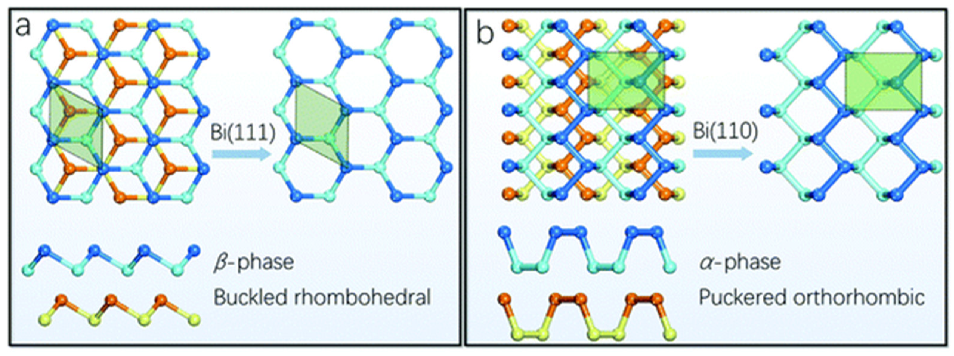
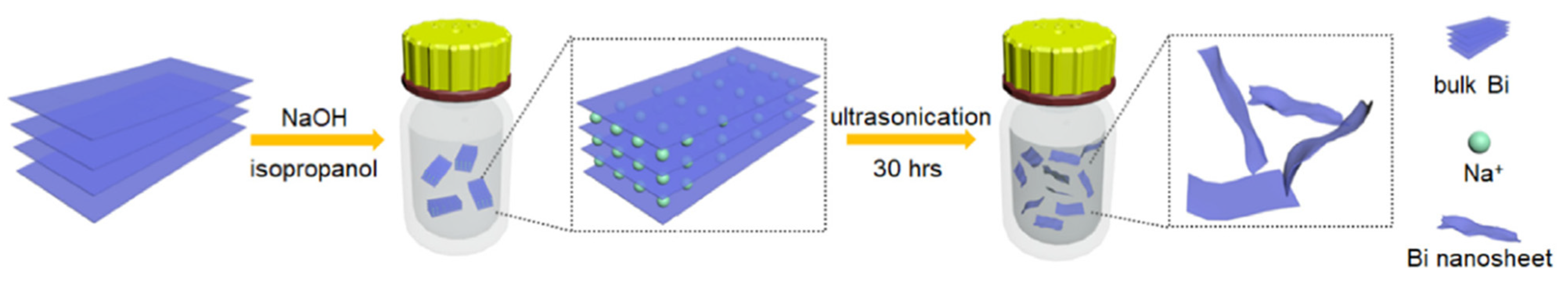
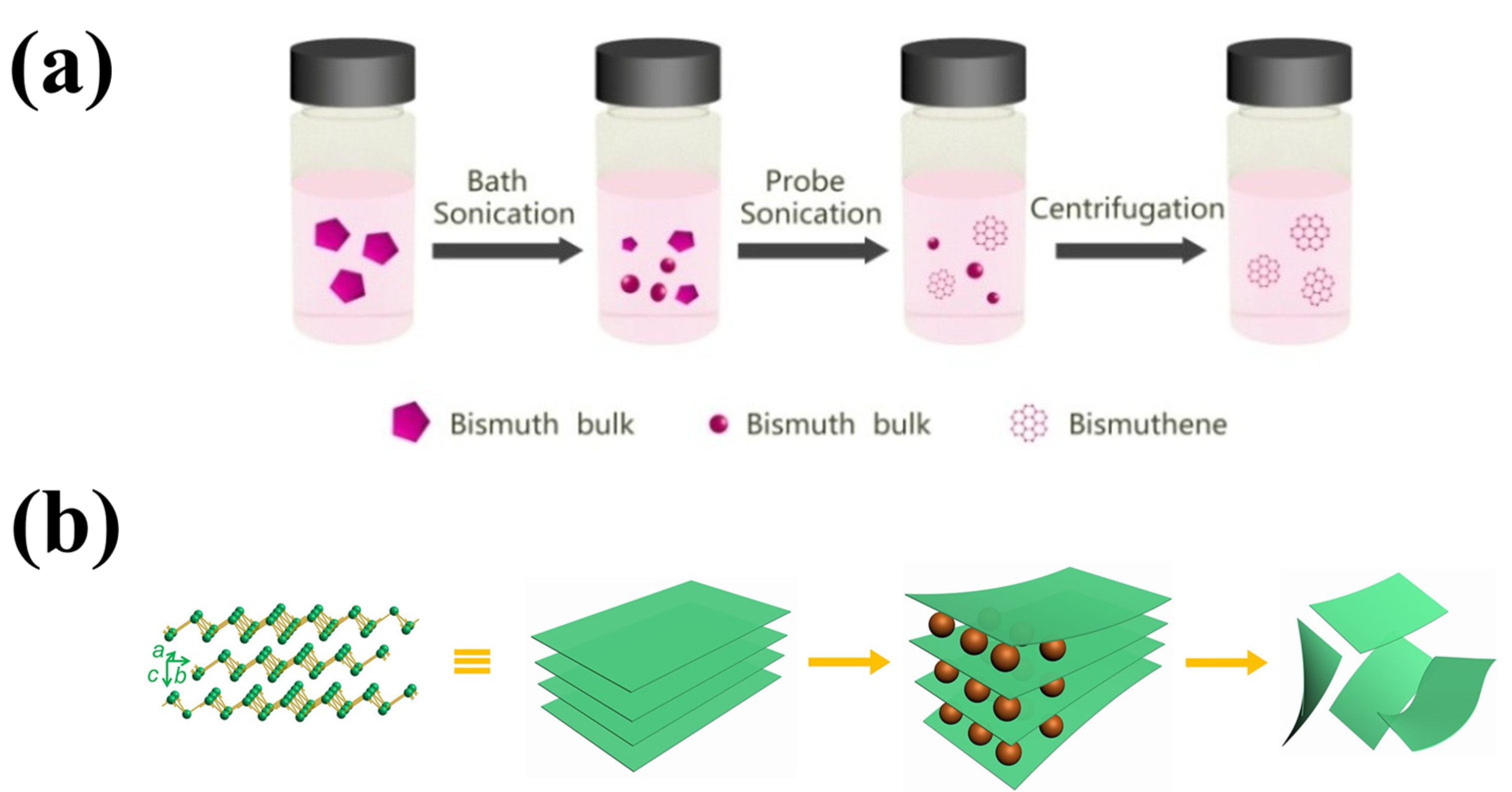

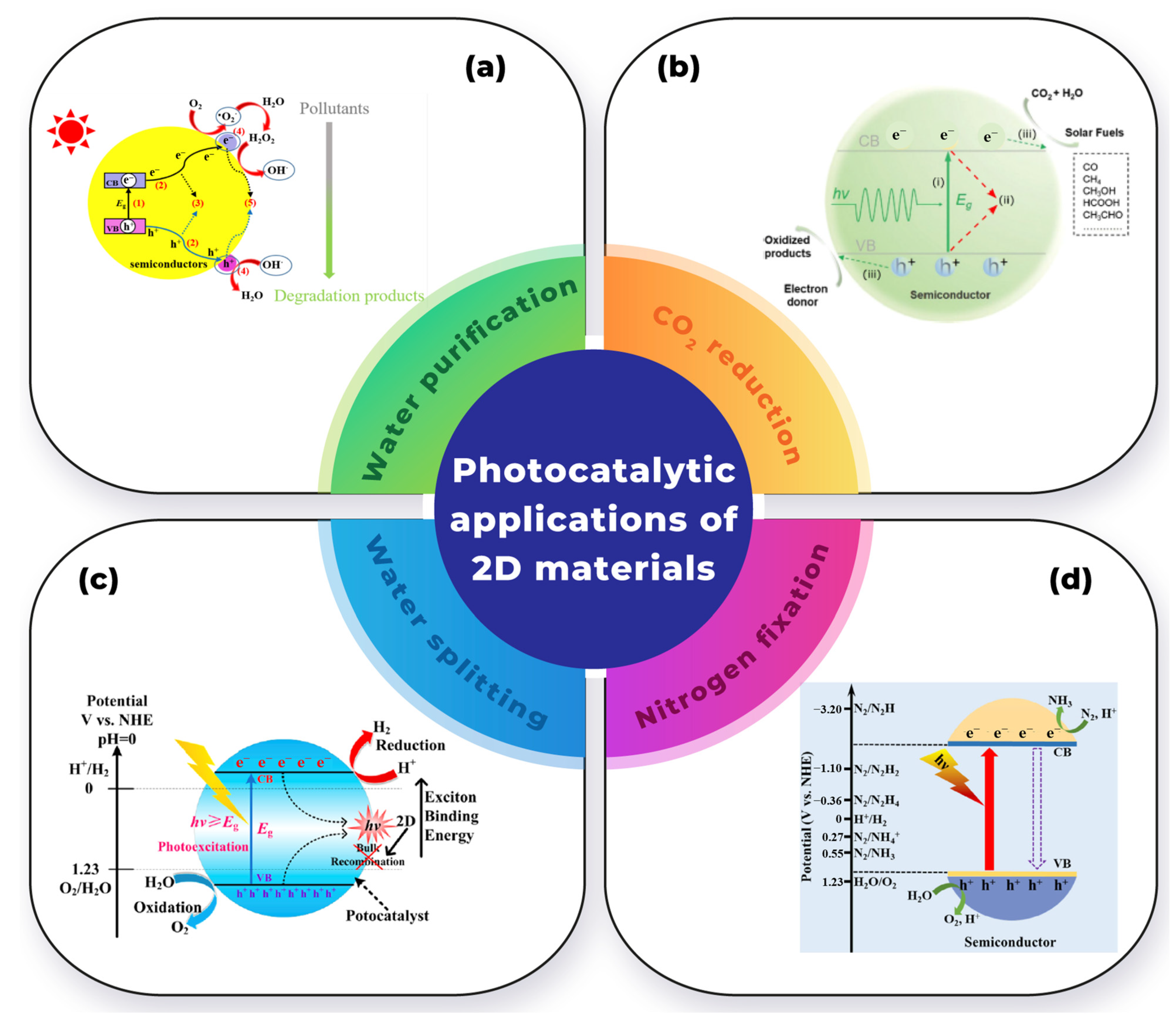
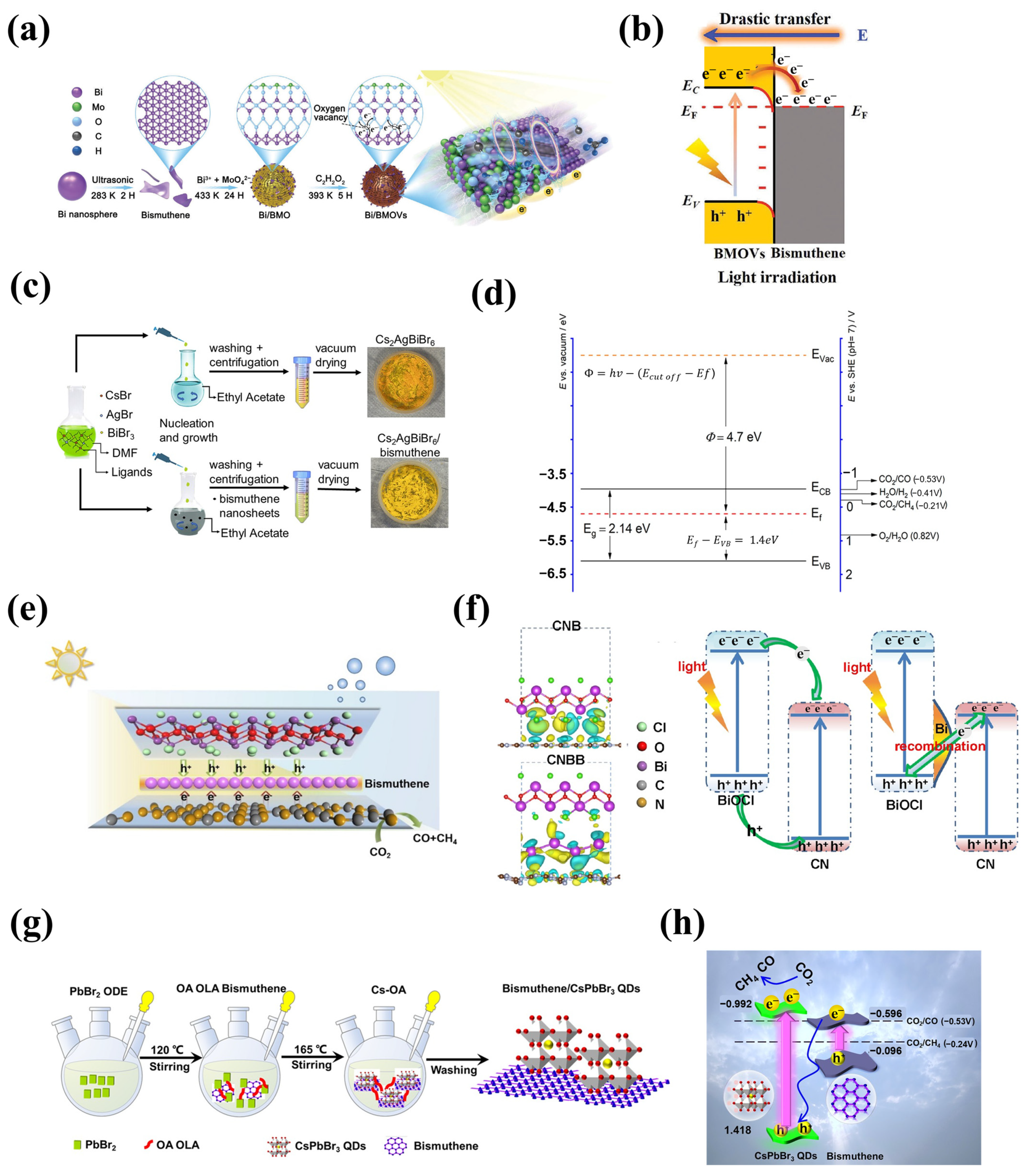

Disclaimer/Publisher’s Note: The statements, opinions and data contained in all publications are solely those of the individual author(s) and contributor(s) and not of MDPI and/or the editor(s). MDPI and/or the editor(s) disclaim responsibility for any injury to people or property resulting from any ideas, methods, instructions or products referred to in the content. |
© 2024 by the authors. Licensee MDPI, Basel, Switzerland. This article is an open access article distributed under the terms and conditions of the Creative Commons Attribution (CC BY) license (https://creativecommons.org/licenses/by/4.0/).