Abstract
Diodes with an erbium and nitrogen codoped magnesium zinc oxide (MgZnO:Er,N) active layer were fabricated by spray pyrolysis on Si substrate with aqueous solutions including magnesium nitrate, zinc acetate, erbium acetate, ammonium acetate, and indium nitrate precursors. Diodes with different nitrogen content in their precursor were prepared and their properties were investigated. With scanning electron microscopy, film surface with mixed hexagonal flakes and tiny blocks was characterized for all samples. Certain morphologies varied for samples with different N contents. In the photoluminescence analyses, the intensity of the oxygen-related defects peak increased with the increasing of nitrogen content. The diodes were fabricated with an Au and In deposition on the top and backside. The diode current–voltage as well as capacitance–voltage characteristics were examined. An ununiformed n-type concentration distribution with high concentration near the interface in the MgZnO:Er,N layer was characterized for all samples. Diodes with high nitrogen content exhibit reduced breakdown voltage and higher interface concentration characteristics. Under reversed bias conditions with an injection current of 50 mA, a light spectrum with two distinct green emissions around wavelengths 532 and 553 nm was observed. A small spectrum variation was characterized for diodes prepared from different nitrogen content. The diode luminescence characteristics were examined and the diode prepared from N/Zn=1 in the precursor showed an optimal injection current-to-luminescence property. The current and luminescence properties of the diode were characterized and discussed.
1. Introduction
Zinc oxide (ZnO), a group II–VI material, has been widely investigated in the past decades. Many zinc oxide based devices, such as sensors [1,2], electronic [3,4], optoelectronic [5,6], and mechanic electronic [7,8] have been studied and applied. One of the optoelectronic diodes, the n-type erbium (Er) doped ZnO on a p-type Si substrate, demonstrates green light luminescence ability [9]. As the emission wavelength is just under the low transmission loss window of the PMMA (Poly(methyl methacrylate) core optical fiber [10], the Er doped ZnO diode shows the developing potential for Si-based photonic devices.
In the Er doped diode, the energy transformation of carriers from impact ionization to Er ions was the origin of diode luminescence. The avalanched breakdown operation conditions for achieving carrier impact ionization herein becomes important. On the other hand, the Er shows an n-type dopant in ZnO with the substation of the Zn site. Thus for the active layer with Er doping, the n-type concentration increases with the increasing of the Er doping. As the Er doped region in the pn diode dominates the diode breakdown conditions, controlled carrier concentrations in the Er doped diode under sufficient Er doping becomes important. In regarding the dopings with the Er-containing materials, much work was performed on their energy transfer mechanism [11,12,13,14,15], but there was less discussion regarding the carrier concentration. Zhong [16] prepared Er doped and Er,N codoped ZnO by implantation and found the luminescence difference by forming Er-O-N complexes. In our previous studies, diode performance improved with Mg incorporated in the pn diode structure [17]. In this diode, the Er-related luminescence was operated under reverse bias with the impact ionization occurring in the depletion region. As the Er (III) doping in ZnO and MgZnO (II–VI) shows an n-type contributor, sufficient Er doping could imply that the depletion width decreased with the increase of n-type concentration. On the other hand, the N shows p-type doping in ZnO [18] and MgZnO [19]. The N doping in the Er content pn diode may compensate for the electron concentration and for the extending of the depletion width of the diode. In this work, the effect of nitrogen doping on the diode was studied. The Er and N codoped MgZnO diode was prepared with different N contents, and we compared the luminescence and diode properties.
2. Experimental Section
The MgZnO:Er,N active layer followed by a ZnO:In layer were deposited on p-type Si substrate (concentration 5 × 1018cm−3) at 450 °C using a spray pyrolysis deposition system with zinc acetate dehydrate (Zn(CH3COO)2·2H2O,0.2M), magnesium acetate tetrahydrate (Mg(CH3COO)2·4H2O)(Mg/Zn=25%), erbium acetate hydrate (Er(CH3COO)3·4H2O)(Er/Zn=5%), and ammonium acetate (CH3COONH3) aqueous solution precursors. Before deposition, the Si wafer was cleaned with acetone, rinsed in DI water, dried by N2 gas, dipped in diluted HF, rinsed in DI water, and dried by N2 gas sequentially. The Si substrate was transferred to the deposition chamber and an approximately 350 nm MgZnO:Er,N layer followed by an approximately 140 nm ZnO:In layer were deposited sequentially. The circular Au electrode with a diameter of 0.8 mm was defined on the ZnO:In side with a metal mask by sputtering. The In contact was formed over the Si backside using a thermal process. Samples with different N/Zn atomic ratios of 0,1,4, and 8 in precursor were prepared and the sample codes were ME, ME1, ME4, and ME8, respectively.
The surface morphology of the samples was examined by scanning electron microscopy (SEM, Hitachi S-4300N, Tokyo, Japan). The elements of the film were analyzed by an energy dispersive X-ray spectrometer (EDS, JEOL JSM-6700F, Tokyo, Japan). The crystalline structure was obtained using X-ray diffraction (XRD, Bruker D8, Billerica, MA, USA). The photoluminescence (PL) spectrum was obtained by an optical system with a spectrometer (HR2000+, Ocean Optics, Largo, FL, USA), He-Cd laser (325 nm wavelength), and a cryostat. The diode current–voltage (I–V), electroluminescence (EL) and capacitance–voltage (C–V) characteristics were examined by a source meter (Keithley 2400, Solon, OH, USA), a spectrometer, and an impedance analyzer (Agilent 4294A, Lexington, MA, USA), respectively.
3. Results and Discussions
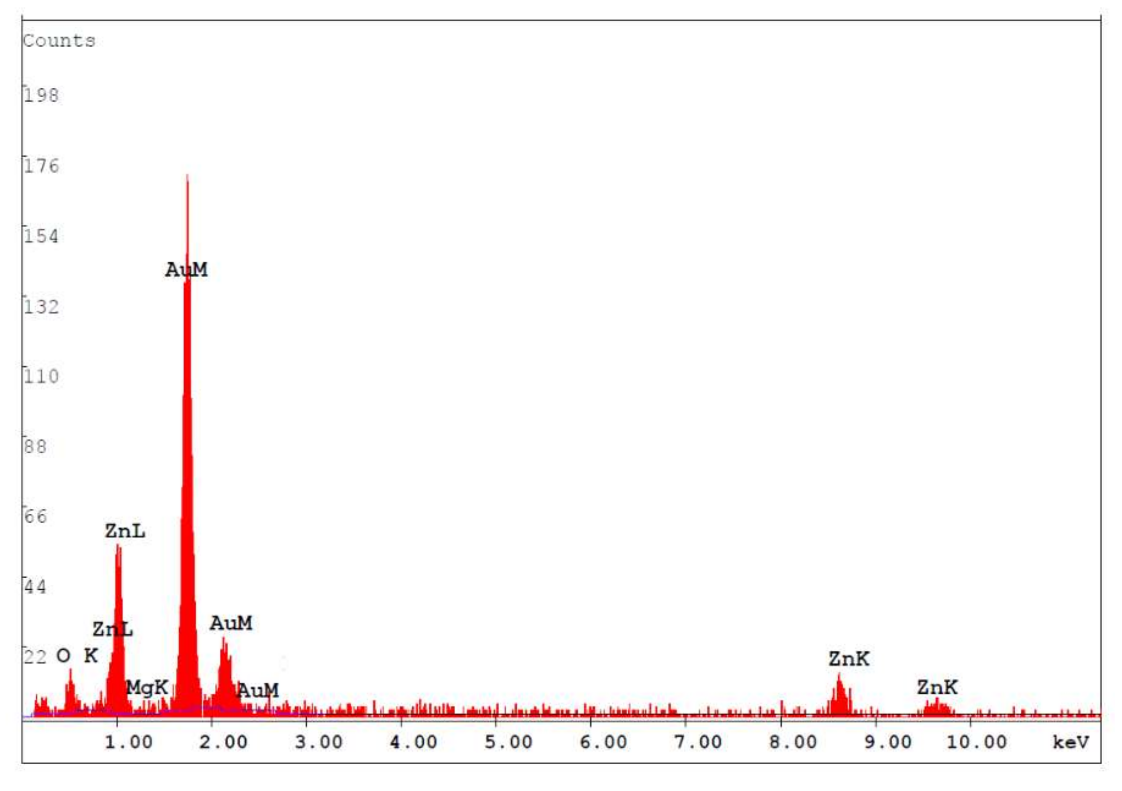
Figure 1 shows the surface morphology of the MgZnO:Er,N diodes: (a) ME, (b) ME1, (c) ME4, and (d) ME8. Granular morphology with stacked hexagonal flakes combined with small blocks can be observed. With the increase of N content in the MgZnO:Er,N layer, the hexagonal flakes become large and the density of the small blocks increases. This surface texture shows a general morphology which is similar to film prepared by spray pyrolysis with zinc acetate precursor [20]. Figure 2 shows the EDS analysis of the MgZnO layer of sample ME. A Mg/Zn atomic ratio of around 10% was achieved.
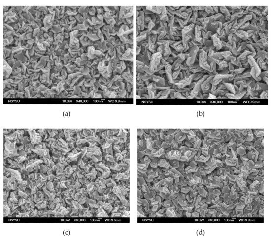
Figure 1.
Surface morphology of MgZnO:Er,N diodes: (a) ME, (b) ME1, (c) ME4, and (d) ME8.

Figure 2.
EDS of the MgZnO layer of sample ME.
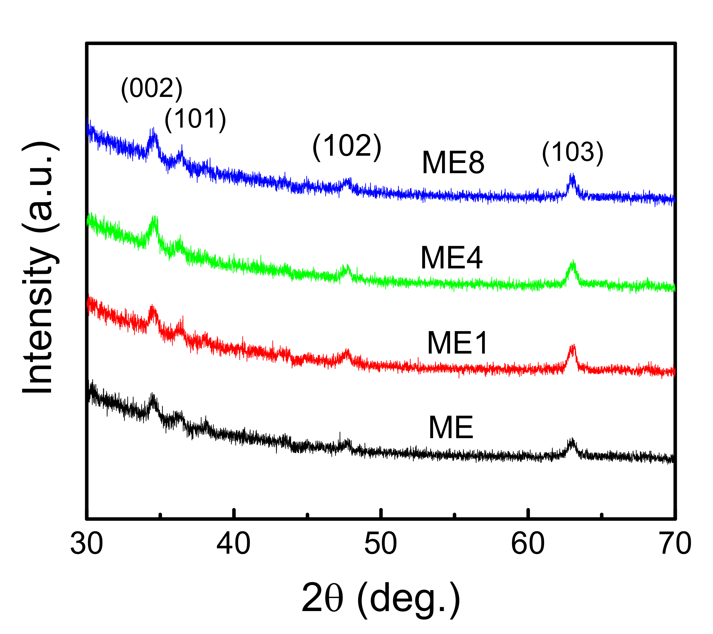
Figure 3 shows the XRD pattern of the samples. The observed peaks at 34.64, 36.39, 47.76, and 63.01 degrees were attributed to wurtzite ZnO-related (002), (101), (102), and (103) planes, respectively. The full width half maximum (FWHM) is broad for all peaks. This is caused by the granular size effect [21] and the incorporated Mg species [22]. With the increase in N content, the intensity of (002) increased slightly and the little crystalline property varied.

Figure 3.
The XRD patterns of samples ME, ME1, ME4, and ME8.
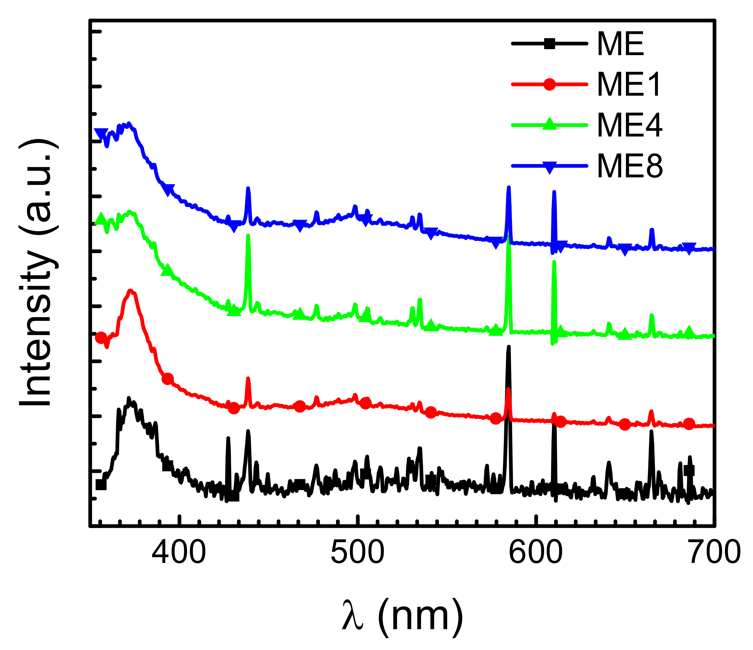
Figure 4 shows the PL spectrum of the samples measured at room temperature. A broad peak around 377 nm can be observed. This is attributed to the near band edge signals of ZnO. In the examined structures, as the band gap of ZnO is less than that of MgZnO, carriers excited by high energy photons under photoluminescence analysis transfer thermally and recombine in the low bandgap ZnO region. The ZnO-related emissions were then characterized. With the increase of N content in the active layer, blue emission with a wavelength around 480–540 nm can be observed. This broad signal is attributed to oxygen-related defects as well as oxygen-interstitial defects, oxygen deficiencies, and a singly ionized oxygen vacancy center [23,24]. Thus, the oxygen-related defects arise in the structure with the introduction of N incorporated in the Er doped layer. On the other hand, the Er-related electroluminescence is attributed to the carrier impact excitation of Er ions [25]. As the photoluminescence emissions originate from the energy transformation by the electron-hole pairs generated after photon excitation, no Er-related photoluminescence emissions in the visible band were observed in the PL measurement [9].

Figure 4.
Photoluminescence spectrum for samples ME, ME1, ME4, and ME8 measured at room temperature.
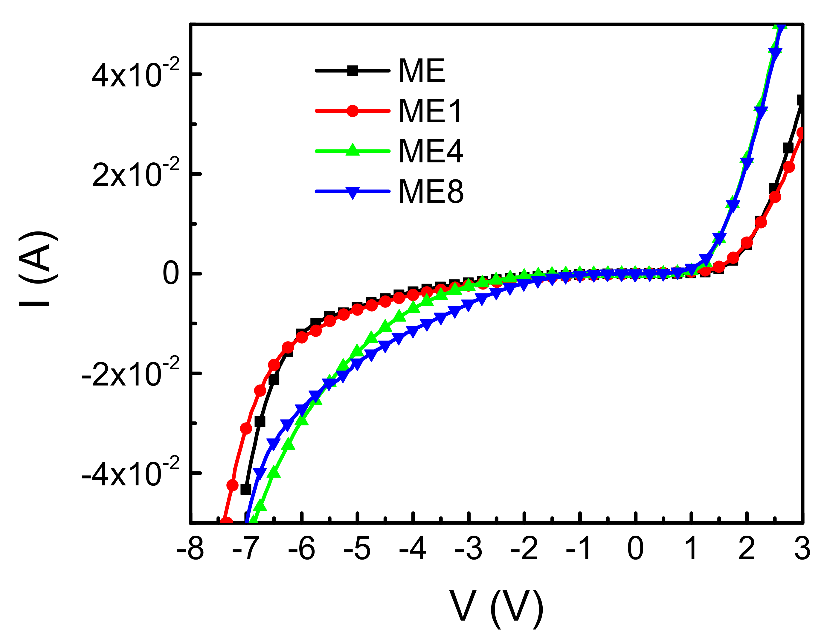
Figure 5 shows the diode current–voltage (I–V) characteristics of the diodes ME, ME1, ME4, and ME8. In the forward bias region, a threshold voltage based on the built-in potential between p-Si and n-MgZnO can be observed. The breakdown characteristics can be observed in the reverse bias region. The operation voltage with reverse biased 30 mA is 6.8 V, 7.0 V, 6.3 V, and 6.5 V for samples ME, ME1, ME4, and ME8, respectively. For samples ME and ME1, the increase of operation voltage is attributed to the n-type concentration reduction in the MgZnO layer caused by introducing the N doping. However, further analysis is necessary to clarify the operation voltage decrease with the continued increase of N content in the MgZnO layer.

Figure 5.
Diode current (I) and voltage (V) characteristics of the diodes ME, ME1, ME4, and ME8.
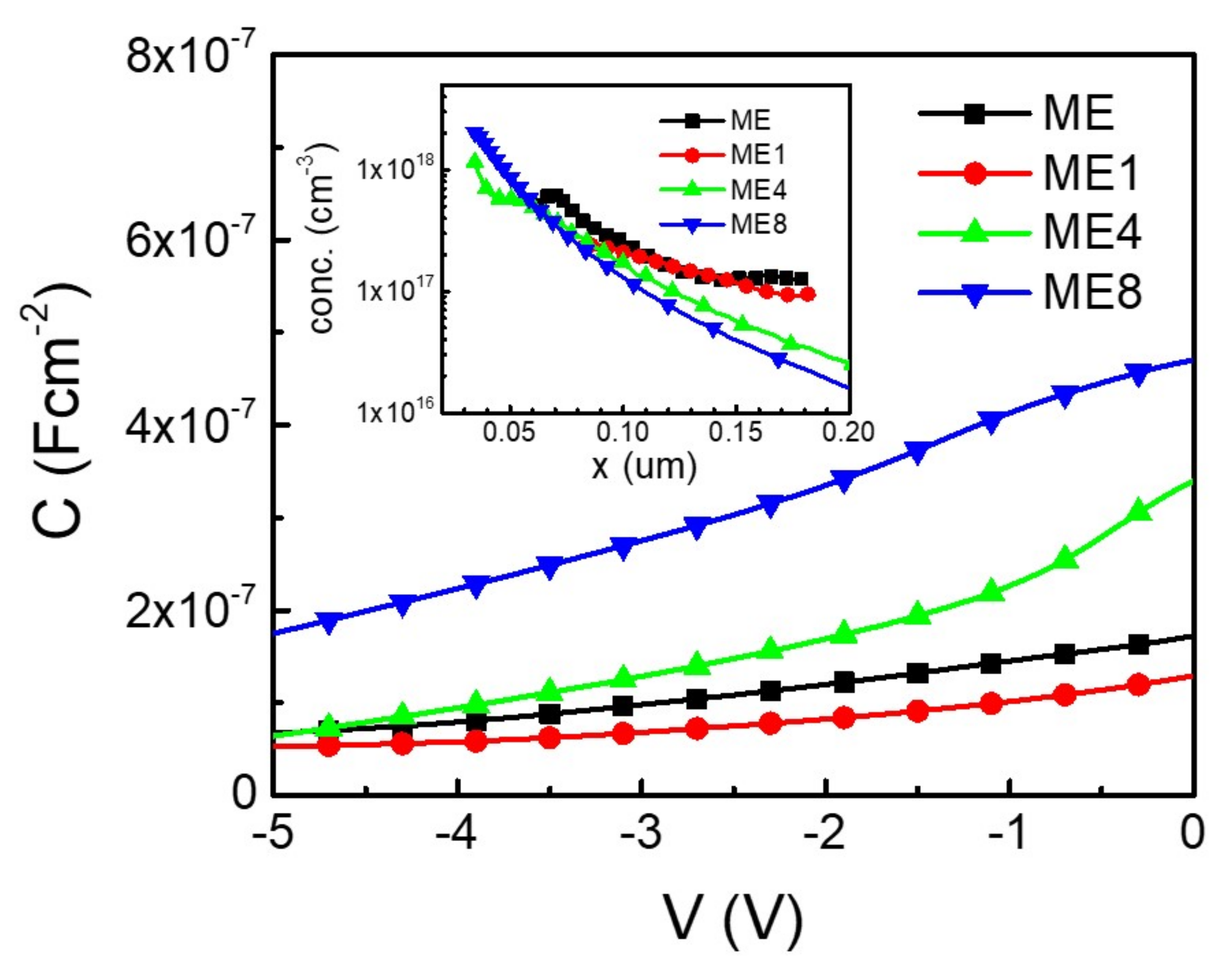
Figure 6 shows the capacitance per area (C) and voltage (V) characteristics of the samples. As the concentration of p-type Si is known (5 × 1019 cm−3), the n-type concentration in MgZnO can thus be characterized from the CV analysis [26]. The inset of the figure shows the concentration (conc.) distribution in the MgZnO layer of the samples while the point of origin (x = 0) is at the p-Si/n-MgZnO interface. It can be seen that the concentration distribution in the MgZnO region is not uniform for all samples, although the supply of precursors for each species remained unchanged in the deposition process. Higher concentration was observed in the MgZnO layer near the Si/MgZnO interface.
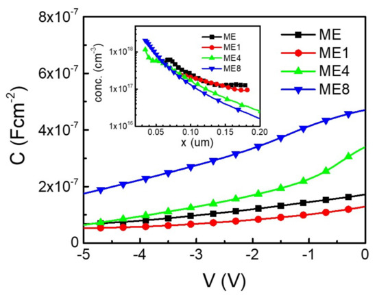
Figure 6.
The diode capacitance (C) and voltage (V) characteristics of the diodes ME, ME1, ME4, and ME8. The inset shows the corresponded carrier concentration (conc.)–position (x) characteristics.
In the deposition of the MgZnO:Er,(N) layer, although the Si substrate was cleaned and the surface oxide was remove using a wet etching process before deposition, a ultrathin oxide layer may have formed during the subsequent deposition of the MgZnO:Er,(N) layer. Interface traps were thus formed by the dangling bonds on the thin oxide layer [27]. Pau et al. examined the ZnO quality spatially on Si substrate. They found that the ZnO near the Si–ZnO interface exhibits higher defect states [28]. For an undoped ZnO, the complex states originate from the pairing of oxygen vacancy (VO) and zinc vacancy (VZn), which takes effect in the carrier concentration [29,30]. In an unintentionally doped ZnO, high n-type concentration may originate from the donor-type of such complex states [30]. In the Si-MgZnO:Er,(N) interface, interface traps with complex states may exist and cause the accumulation of n-type concentration.
In considering the concentration difference in different samples, the concentration decreases with the increasing of N doping in the region far away from interface (x > 0.15). This is due to the carrier compensation effect of N doping [31]. On the other hand, the concentration accumulation characteristics near the interface region were enhanced with the increasing of N doping. As the ammonium acetate aqueous solution precursor was used as the supplier of N dopant, species from thermally decomposed ammonium acetate radicals in deposition process may take effect on the dangling bonds on thin oxide and thus enhance the donor-type defects on the close interface region in the MgZnO:Er,N layer. With more donor-type defects near the interface, a high reverse bias leakage current with a reverse bias excess of −2 V for ME4 and ME8 was realized.
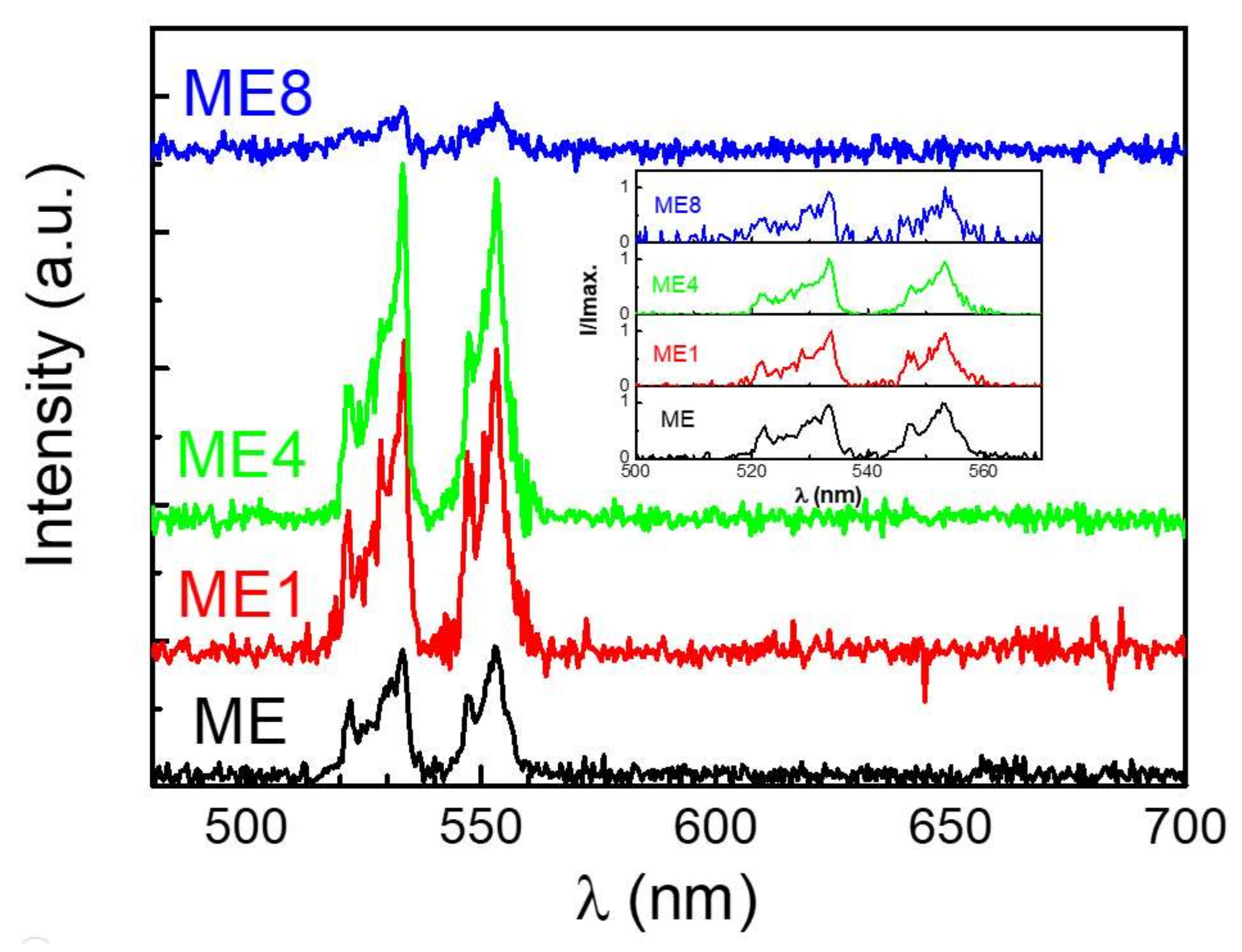
Figure 7 shows the room temperature electroluminescence spectrum of these diodes under an injection current of 50 mA in reverse bias. The inset shows the normalized intensity (I/Imax.) of each diode. For the Er-contained diode, the electrons and holes which were generated and accelerated in the depletion due to a high reverse biased condition may transfer the energy to Er3+ via impact ionization and cause the emissions. Two emission bands around 532 and 553 nm can be observed. The emissions are correlated to the energy state transitions of Er3+ of 2H11/2 → 4I15/2 and 4S3/2→ 4I15/2, respectively, after the impact of the carriers in the MgZnO:Er(,N) layer. When comparing the spectrum of these diodes, little spectrum difference can be observed. Thus some host material variation occurred [32] for the MgZnO:Er,N with nitrogen doping.
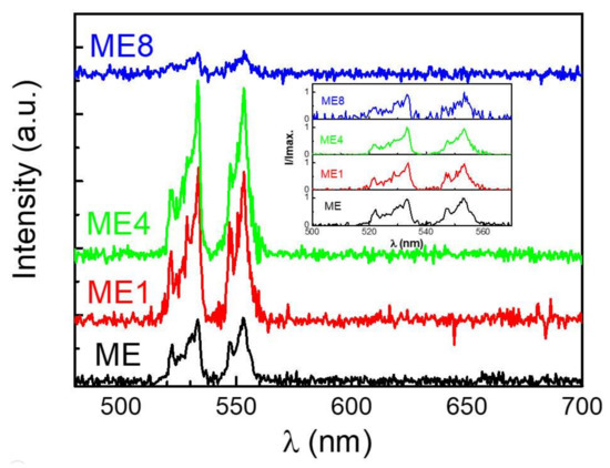
Figure 7.
Electroluminescence emissions of the diodes under a reverse biased 50 mA injection current at room temperature.
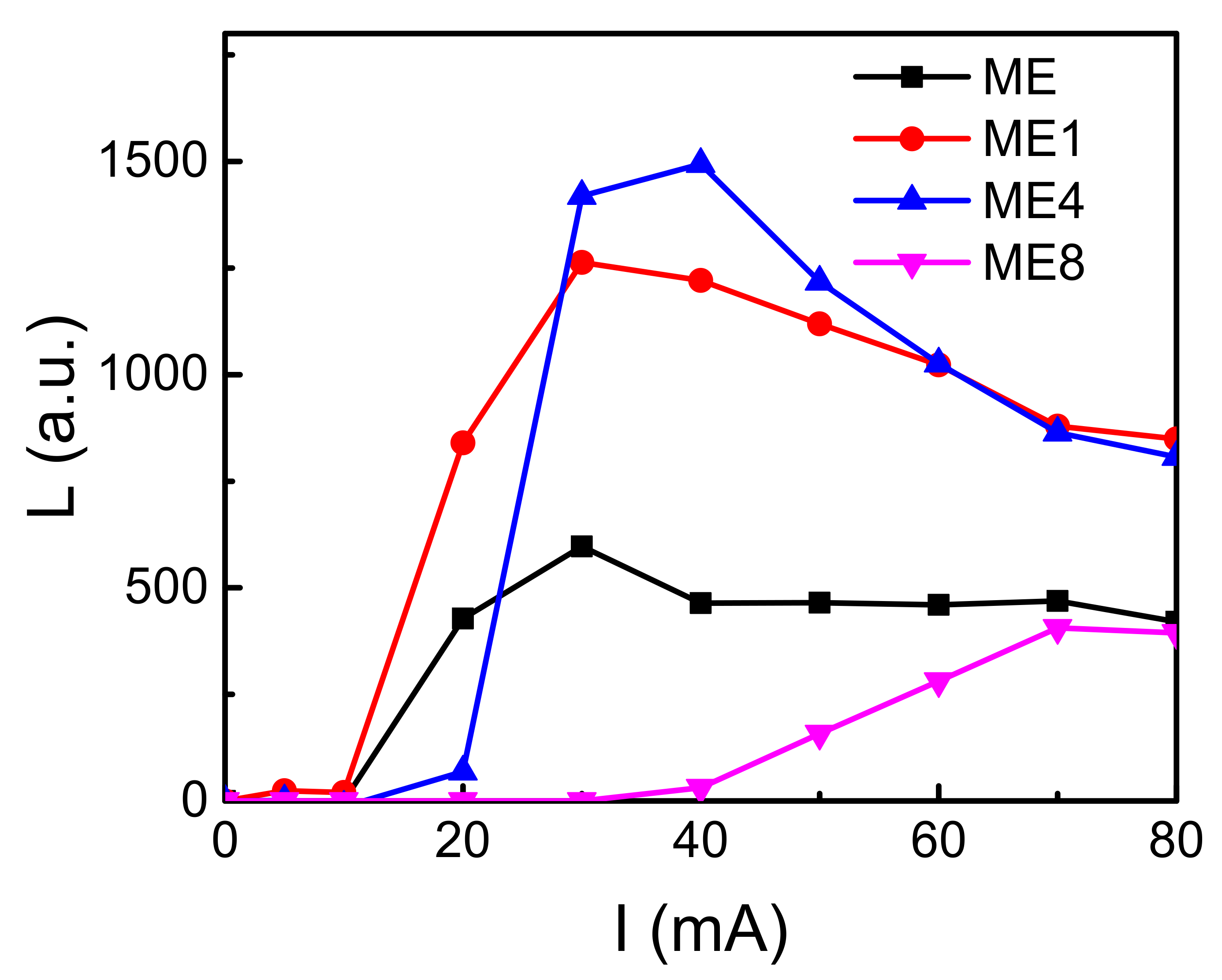
Figure 8 shows the intensity (L)–injection current (I) characteristics of the diodes. The light intensity arose after a certain current injection. This may have been caused by the leakage current before the avalanche breakdown. The leakage current originated from the defect states that may have concentrated around the grain boundaries shown in Figure 1. With the further increase in the current, the light intensity increases due to the increase of the impact ionization current in the depletion region. The light intensity decreased as the current increased further. This originated from the joule heat generated under the high injection current.
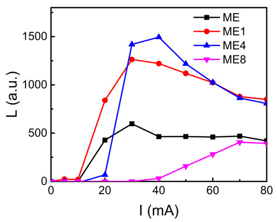
Figure 8.
The intensity (L)–injection current (I) characteristics of the diodes ME, ME1, ME4, and ME8.
The maximum light intensity of these diodes showed an increasing-decreasing behavior with the increasing of N in the active layer. For ME1 and ME4, as the n-type concentration in MgZnO:Er,N reduced, carriers accumulated and transfer energy to the Er ion effectively and caused the light intensity increase. On the other hand, as the varied surface granular morphology and the high donor-like states arise around the Si-MgZnO interface for ME4 and ME8, the increase of leakage current for ME4 and ME8 can be realized.
4. Conclusions
The p-type Si/n-type MgZnO:Er,N/n-type ZnO:In diodes with different N content were prepared by spray pyrolysis. The film surface morphology remained and the O-related defects increased with the increase of N content. The n-type concentration in MgZnO:Er,N layer compensated in the region far away from the Si interface and accumulated in the region near the Si interface with the increase of N content. With high N content, concentration accumulation around the interface, which may originate from donor-type defects, was enhanced and dominated the diode performance with a raised leakage current. The diode luminescence spectrum was examined. Improved luminescence was characterized for the diode prepared with a suitable N/Zn ratio.
Author Contributions
Conceptualization: Y.-T.H., W.-H.L. and K.-F.H.; Methodology: C.-A.C., K.-J.C. and C.-J.H.; Validation: K.-J.C., M.-C.W., C.-J.H.; Formal Analysis: C.-A.C., Y.-T.H. and W.-H.L.; Investigation: W.-H.L.; Data Curation: C.-A.C., Y.-T.H. and W.-H.L.; Writing—Original Draft Preparation: M.-C.W. and W.-H.L.; Writing—Review & Editing: W.-H.L., Visualization: W.-H.L.; supervision, W.-H.L.; project administration, W.-H.L.; funding acquisition, W.-H.L. All authors have read and agreed to the published version of the manuscript.
Funding
This research was funded by Ministry of Science and Technology, Taiwan (MOST 107-2221-E-390-013-), and National Chung Shan Institute of Science and Technology, R.O.C., NCSIST-108.
Acknowledgments
The authors wish to acknowledge the Ministry of Science and Technology, Taiwan and National Chung Shan Institute of Science and Technology, R.O.C. for the financial support.
Conflicts of Interest
The authors declare no conflict of interest.
References
- Zhao, R.; Li, K.; Wang, Z.; Xing, X.; Wang, Y. Gas-sensing performances of Cd-doped ZnO nanoparticles synthesized by a surfactant-mediated method for n-butanol gas. J. Phys. Chem. Solids 2018, 112, 43–49. [Google Scholar] [CrossRef]
- Jagadale, S.B.; Patil, V.L.; Vanalakar, S.A.; Patil, P.S.; Deshmukh, H.P. Preparation, characterization of 1D ZnO nanorods and their gas sensing properties. Ceram. Int. 2018, 44, 3333–3340. [Google Scholar] [CrossRef]
- Medina-Montes, M.I.; Baldenegro-Perez, L.A.; Sanchez-Zeferino, R.; Rojas-Blanco, L.; Becerril-Silva, M.; Quevedo-Lopez, M.A.; Ramirez-Bon, R. Effect of depth of traps in ZnO polycrystalline thin films on ZnO-TFTs performance. Solid State Electron. 2016, 123, 119–123. [Google Scholar] [CrossRef]
- Kim, C.Y.; Park, J.H.; Kim, T.G. Effect of photochemical hydrogen doping on the electrical properties of ZnO thin-film transistors. J. Alloy. Compd. 2018, 732, 300–305. [Google Scholar] [CrossRef]
- Hossaini, H.; Moussavi, G.; Farrokhi, M. Oxidation of diazinon in cns-ZnO/LED photocatalytic process: Catalyst preparation, photocatalytic examination, and toxicity bioassay of oxidation by-products. Sep. Purif. Technol. 2017, 174, 320–330. [Google Scholar] [CrossRef]
- Sandeep, K.M.; Bhat, S.; Dharmaprakash, S.M. Structural, optical, and LED characteristics of ZnO and Al doped ZnO thin films. J. Phys. Chem. Solids 2017, 104, 36–44. [Google Scholar] [CrossRef]
- Raj, V.B.; Singh, H.; Nimal, A.T.; Tomar, M.; Sharma, M.U.; Gupta, V. Origin and role of elasticity in the enhanced DMMP detection by ZnO/SAW sensor. Sens. Actuators B Chem. 2015, 207, 375–382. [Google Scholar] [CrossRef]
- Maouhoub, S.; Aoura, Y.; Mir, A. FEM simulation of Rayleigh waves for SAW devices based on ZnO/AlN/Si. Microelectron. Eng. 2015, 136, 22–25. [Google Scholar] [CrossRef]
- Iwan, S.; Bambang, S.; Zhao, J.L.; Tan, S.T.; Fan, H.M.; Sun, L.; Zhang, S.; Ryu, H.H.; Sun, X.W. Green electroluminescence from an n-ZnO: Er/p-Si heterostructured light-emitting diode. Physica B 2012, 407, 2721–2724. [Google Scholar] [CrossRef]
- Zubia, J.; Arrue, J. Plastic Optical Fibers: An Introduction to Their Technological Processes and Applications. Opt. Fiber Technol. 2001, 7, 101–140. [Google Scholar] [CrossRef]
- Dong, B.; Li, Z.A.; Cao, B.; Yu, N.; Sun, M. Quasi-one dimensional Er3+–Yb3+ codoped single-crystal MoO3 ribbons: Synthesis, characterization and up-conversion luminescence. Opt. Commun. 2011, 284, 2528–2531. [Google Scholar] [CrossRef]
- Prucnal, S.; Rebohle, L.; Skorupa, W. Electroluminescence from Er and Yb co-doped silicon dioxide layers: The excitation mechanism. J. Non Cryst. Solids 2011, 357, 915–918. [Google Scholar] [CrossRef]
- Llusca, M.; Lopez-Vidrier, J.; Antony, A.; Hernandez, S.; Garrido, B.; Bertomeu, J. Up-conversion effect of Er-and Yb-doped ZnO thin films. Thin Solid Film. 2014, 562, 456–461. [Google Scholar] [CrossRef][Green Version]
- Kobwittaya, K.; Oishi, Y.; Torikai, T.; Yada, M.; Watari, T.; Luitel, H.N. Bright red upconversion luminescence from Er3+ and Yb3+ co-doped ZnO-TiO2 composite phosphor powder. Ceram. Int. 2017, 43, 13505–13515. [Google Scholar] [CrossRef]
- Meng, X.; Liu, C.; Wu, F.; Li, J. Strong up-conversion emissions in ZnO: Er3+, ZnO: Er3+–Yb3+ nanoparticles and their surface modified counterparts. J. Colloid Interface Sci. 2011, 358, 334–337. [Google Scholar] [CrossRef]
- Zhong, K.; Xu, J.; Su, J.; Chen, Y.L. Upconversion luminescence from Er-N codoped of ZnO nanowires prepared by ion implantation method. Appl. Surf. Sci. 2011, 257, 3495–3498. [Google Scholar] [CrossRef]
- Hsu, Y.T.; Lee, C.C.; Lan, W.H.; Huang, K.F.; Chang, K.J.; Lin, J.C.; Lee, S.Y.; Lin, W.J.; Wang, M.C.; Huang, C.J. Thickness Study of Er-Doped Magnesium Zinc Oxide Diode by Spray Pyrolysis. Crystals 2018, 8, 454. [Google Scholar] [CrossRef]
- Chakrabarti, S.; Doggett, B.; O’Haire, R.; McGlynn, E.; Henry, M.O.; Meaney, A.; Mosnier, J.P. p-type conduction above room temperature in nitrogen-doped ZnO thin film grown by plasma-assisted pulsed laser deposition. Electron. Lett. 2006, 42, 1181–1182. [Google Scholar] [CrossRef]
- Lin, T.Y.; Hsu, Y.T.; Chen, L.C.; Wang, M.C.; Hsu, W.H.; Lee, C.Y.; Huang, S.C.; Ding, Y.X.; Huang, K.F.; Lan, W.H. Conductivity Study of Nitrogen-Doped Magnesium Zinc Oxide Prepared by Spray Pyrolysis. Mater. Focus 2015, 4, 1–4. [Google Scholar] [CrossRef]
- Krunks, K.; Bijakina, O.; Mikli, V.; Varema, T. Zinc Oxide Thin Films by Spray Pyrolysis Method. Phys. Scr. 1999, 79, 209–212. [Google Scholar] [CrossRef]
- Benhaliliba, M.; Benouis, C.E.; Aida, M.S.; Yakuphanoglu, F.; Juarez, A.S. Indium and aluminium-doped ZnO thin films deposited onto FTO substrates: Nanostructure, optical, photoluminescence and electrical properties. J. Sol Gel Sci. Technol. 2010, 55, 335–342. [Google Scholar] [CrossRef]
- Kim, Y.Y.; Kong, B.H.; Choi, M.K.; Cho, H.K. Influence of Mg composition on the characteristics of MgZnO/ZnO heterostructures grown by co-sputtering. Mater. Sci. Eng. B 2009, 165, 80–84. [Google Scholar] [CrossRef]
- Pal, S.; Gogurla, N.; Das, A.; Singha, S.S.; Kumar, P.; Kanjilal, D.; Singha, A.; Chattopadhyay, S.; Jana, D.; Sarkar, A. Clustered vacancies in ZnO: Chemical aspects and consequences on physical properties. J. Phys. D Appl. Phys. 2018, 51, 105107. [Google Scholar] [CrossRef]
- Wahyuono, A.R.; Hermann-Westendorf, F.; Dellith, A.; Schmidt, C.; Dellith, J.; Plentz, J.; Schulz, M.; Presselt, M.; Seyring, M.; Rettenmeyer, M. Effect of annealing on the sub-bandgap, defects and trapping states of ZnO nanostructures. Chem. Phys. 2017, 483, 112–121. [Google Scholar] [CrossRef]
- Harako, S.; Yokoyama, S.; Ide, K.; Zhao, X.; Komoro, S. Visible and infrared electroluminescence from an Er-doped n-ZnO/p-Si light emitting diode. Phys. Status Solidi A 2008, 205, 19–22. [Google Scholar] [CrossRef]
- Sze, S.M.; Lee, M.K. Semiconductor Devices, 3rd ed.; John Wiley & Sons Inc.: Hoboken, NJ, USA, 2012; pp. 95–97. ISBN 978-0470-53794-7. [Google Scholar]
- Li, C.Y.; Cheng, M.Y.; Houng, M.P.; Yang, C.F.; Liu, J. Electric Characteristic Enhancement of an AZO/Si Schottky Barrier Diode with Hydrogen Plasma Surface Treatment and AlxOx Guard Ring Structure. Materials 2018, 11, 90. [Google Scholar] [CrossRef]
- Pau, J.L.; Piqueras, J.; Rogers, D.J.; Teherani, F.H.; Minder, K.; McClintock, R.; Razeghi, M. On the interface properties of ZnO/Si electroluminescent diodes. J. Appl. Phys. 2010, 107, 033719. [Google Scholar] [CrossRef]
- Weidinger, A.; Gil, J.M.; Alberto, H.V.; Vilão, R.C.; Duarte, J.P.; de Campos, N.A.; Cox, S.F.J. Shallow donor versus deep acceptor state in II–VI semiconductor compounds. Physica B 2003, 326, 124–127. [Google Scholar] [CrossRef]
- Krzywiecki, M.; Grzadziel, L.; Sarfraz, A.; Iqbal, D.; Szwajca, A.; Erbe, A. Zinc oxide as a defect-dominated material in thinfilms for photovoltaic applications-experimental determination of defect levels, quantification of composition, and construction of band diagram. Phys. Chem. Chem. Phys. 2015, 17, 10004–10013. [Google Scholar] [CrossRef]
- Li, L.; Shan, C.X.; Li, B.H.; Yao, B.; Zhang, J.Y.; Zhao, D.X.; Zhang, Z.Z.; Shen, D.Z.; Fan, X.W.; Lu, Y.M. The compensation source in nitrogen doped ZnO. J. Phys. D Appl. Phys. 2008, 41, 245402. [Google Scholar] [CrossRef]
- Polman, A. Erbium as a probe of everything? Physica B 2001, 300, 78–90. [Google Scholar] [CrossRef]
© 2020 by the authors. Licensee MDPI, Basel, Switzerland. This article is an open access article distributed under the terms and conditions of the Creative Commons Attribution (CC BY) license (http://creativecommons.org/licenses/by/4.0/).


