Review

Heteroepitaxial Growth of III-V Semiconductors on Silicon

Department of Electronic and Electrical Engineering, University College London, Torrington Place, London WC1E 7JE, UK
*
Authors to whom correspondence should be addressed.
Crystals 2020, 10(12), 1163; https://doi.org/10.3390/cryst10121163
Submission received: 6 November 2020 / Revised: 14 December 2020 / Accepted: 14 December 2020 / Published: 21 December 2020
(This article belongs to the Special Issue Semiconductor Heteroepitaxy)

Abstract

:
Monolithic integration of III-V semiconductor devices on Silicon (Si) has long been of great interest in photonic integrated circuits (PICs), as well as traditional integrated circuits (ICs), since it provides enormous potential benefits, including versatile functionality, low-cost, large-area production, and dense integration. However, the material dissimilarity between III-V and Si, such as lattice constant, coefficient of thermal expansion, and polarity, introduces a high density of various defects during the growth of III-V on Si. In order to tackle these issues, a variety of growth techniques have been developed so far, leading to the demonstration of high-quality III-V materials and optoelectronic devices monolithically grown on various Si-based platform. In this paper, the recent advances in the heteroepitaxial growth of III-V on Si substrates, particularly GaAs and InP, are discussed. After introducing the fundamental and technical challenges for III-V-on-Si heteroepitaxy, we discuss recent approaches for resolving growth issues and future direction towards monolithic integration of III-V on Si platform.

1. Introduction

Silicon (Si) has long been of great importance in a wide range of micro/nanoelectronics industry because it offers numerous benefits, such as large wafer size, low cost, abundant source, and mature manufacturing technology [1]. Indeed, for instance, Si-based complementary metal-oxide-semiconductor (CMOS) technology is the fundamental building block in most of the contemporary electronics [2,3], and Si has also been one of the dominant prime materials for photovoltaic technology since the 1950s [4]. More importantly, the utility of Si has expanded from traditional electronics to next-generation photonics industry as Si photonics, enabling ultra-fast and low-cost optical data transmission on Si-on-insulator (SOI) platform compatible with a CMOS process, has emerged recently [5]. Unfortunately, however, bulk Si material is an indirect bandgap semiconductor and hence very inefficient for light emission. Although Si-based light-emitting devices, such as Si Raman laser [6,7] and p-n junction emitter [8,9,10], have been developed, their performances are impractical and far less than those of III-V devices [11,12]. On the other hand, most III-V semiconductors provide superior optoelectronic properties owing to their direct bandgap and high electron mobility properties. These advantages enable the III-V semiconductors to be widely used in light-emitting/absorbing devices, including light-emitting diodes (LEDs), lasers, detectors, and solar cells [13,14,15,16]. In addition, the III-V materials have been employed for power devices, such as high electron mobility transistor (HEMT) [17,18]. However, the limited wafer size of III-V materials (3 or 4 inch), which increases manufacturing cost, is a critical drawback. In addition, the use of III-V semiconductors requires careful attention due to their toxicity [19], and despite the advances in the InP-based PICs [20,21], the III-V foundry still lacks mature electronic and photonic platforms compared with the Si-based platforms [5,22].
In order to leverage the benefits of both Si (low-cost, large wafer size, and advanced manufacturing technology) and III-V (optoelectronic properties), a heteroepitaxial growth of III-V semiconductors on Si substrates has been extensively investigated since the 1980s [23,24,25,26,27,28,29]. In addition, the III-V-on-Si heteroepitaxy has opened the possibility of the monolithic integration of III-V devices on Si-based platform which offers new functionality, low-cost, and dense integration in next-generation photonic integrated circuits (PICs), as well as traditional integrated circuits (ICs) [5,30,31]. For example, to overcome the downscaling limit of conventional CMOS technology, monolithic integrations of various III-V devices, such as InGaAs-based channel field-effect transistor (FET), InP heterojunction bipolar transistor (HBT), and GaN HEMT, have been proposed, enabling dense 3-dimensional integration, low power consumption, and high-speed [32,33,34]. Notwithstanding the tremendous efforts on III-V-on-Si heteroepitaxy, however, the monolithic integration of III-V devices on Si-based PICs or ICs is not deployed yet, mainly due to the material dissimilarities between III-V and Si introducing a high density of defects, such as antiphase boundaries (APBs) and threading dislocations (TDs) [24,26]. These defects significantly degrade the performance or even prevent the operation of III-V devices. Hence, to avoid the negative influence of high density of defects, most of the current integration processes between III-V and Si commonly adopt heterogeneous approaches using III-V epitaxial layer or devices grown on their native substrates [35,36]. In general, the heterogeneous integration can be achieved by either flip-chip or wafer bonding. The flip-chip bonding process easily integrates the pre-fabricated III-V devices on Si by using solder bump, but it suffers from the requirement of accurate alignment and the limited integration density [12,37]. In case of wafer bonding, a wide range of approaches, such as eutectic bonding [38], adhesive bonding [39,40], solder bonding [41], direct bonding [42,43,44,45], and so on [36,46], have been developed. For instance, Si photonics, in which Si-based monolithic light source remains as a missing component over decades, typically adopts plasma-assisted direct bonding of III-V die on SOI platform [47]. Although the III-V quantum-dot (QD) lasers monolithically grown on Si have been successfully demonstrated in recent years [48,49,50,51,52,53], the integration-incompatibility with other photonic components impedes the deployment on PICs; thus, heterogeneous integration of III-V lasers is the dominant approach in current Si photonics technology. However, the heterogeneous integration still suffers from high manufacturing cost and low integration density [54]. This is mainly due to the inherent limitation of using III-V native substrates. The size and cost of III-V native substrates are much smaller and higher than those of Si substrates, respectively [55]. Therefore, it is crucial to achieve monolithic integration of III-V/Si which enables cost-effective and dense integration.
In this regard, growing high-quality III-V semiconductors on Si is a key pathway towards monolithic integration of III-V devices on Si-based PICs or ICs. For high-quality III-V layer on Si, the main challenges, namely the high density of various defects caused by material dissimilarities, such as large lattice mismatch, polar-on-nonpolar growth, and different coefficient of thermal expansion, should be tackled [12]. Above all, it is prerequisite to prevent the formation of APBs. This is because the APBs nucleated at the interface between III-V and Si can propagate through whole III-V overlayer, and thus the presence of APBs makes it impossible to fabricate the devices [56]. It is also important for high-performance devices to reduce the density of TDs, which act as nonradiative recombination centers and leakage path [28].
In this review, we discuss the recent advances in the heteroepitaxial growth of III-V on Si substrates and focus on the growth of GaAs and InP, which are particularly important materials for laser applications. The growth of III-nitride materials on Si, closely related to the field of LEDs and HEMT, is excluded in this review, and the recent overview of nitride-on-Si can be found in following articles [57,58,59]. In addition, the dilute nitride materials, such as GaNAsP, have attracted considerable interest recently because of their advantages, such as the direct bandgap property and the lattice-matched growth on Si [60]. Particularly, the growth of lattice-matched GaNAsP-based materials on Si or GaP/Si eliminates an issue of the generation of misfit and threading dislocations [61]. Therefore, the GaNAsP-based materials are very promising for the monolithic integration of optoelectronic devices on Si-based platform. Indeed, substantial progress has been made in the development of GaNAsP-based photovoltaic cells and lasers monolithically grown on Si-based platform [61,62,63,64,65,66,67]. Although the growth of dilute materials on Si is an emerging field in terms of monolithic integration, the physics and growth are quite different from III-V (GaAs and InP), thereby the growth of dilute materials on Si is excluded in this review. The overview for dilute material can be found elsewhere [60,61,68,69].
After a brief introduction to the challenges for III-V-on-Si heteroepitaxy, recent approaches for growing high-quality III-V materials on Si will be addressed: (1) APB-free III-V growth on CMOS-compatible on-axis (001) Si substrates; (2) strategies for reducing the threading dislocation density (TDD); and (3) minimization of thermal cracks. Finally, we summarize the current status and discuss the potential future of III-V-on-Si heteroepitaxy.

2. Fundamental Challenges for III-V Heteroepitaxy on Si

Despite the technological advances in the heterogeneous integration of III-V devices on Si-based platform, monolithic integration, in the long term, is considered as the most promising solution to tackle the limits of current ICs and PICs technology. For the practical implementation of monolithic integration, it is prerequisite to resolve the fundamental problems of III-V-on-Si heteroepitaxy, including APBs, TDs, and thermal crack. In this section, these fundamental challenges which stem from the difference in material properties between III-V and Si will be introduced.

2.1. Antiphase Boundary

First, the formation of APBs arising from the polar on nonpolar nature of III-V/Si heteroepitaxy and monatomic step of (001) Si surface is a critical issue [56,70]. For the vicinal Si(001) surface, a slight misorientation (less than 2°~3°) with respect to the [001] direction in the [ 110 ] and [ 1 ¯ 10 ] direction, corresponding to the direction of dimer rows, causes monatomic steps [71,72,73,74]. Due to the symmetry of diamond structure, two types of steps, running parallel (A-type straight step) and perpendicular (B-type ragged step) to the dimer rows of the upper terrace, can be found on the vicinal Si(001) surface. Indeed, the neighboring terraces consist of two alternating (2 × 1) and (1 × 2) domains. In the zinc-blende structure, e.g., GaAs, InP, and GaP, two face-centered-cubic sublattices are occupied by different atoms. Therefore, if this allocation is changed, the domain with opposite sublattice allocation creates a planar defect called APBs or inversion boundaries (IBs). The domains separated by APBs are known to be antiphase domains (APDs). As shown in Figure 1, for example, monatomic steps on the (001) Si surface result in APDs in the III-V overlayer which are separated by APBs consisting of either III-III or V-V bonds [75]. Even though the formation of wrong bonds across the APBs is energetically unfavorable, this can be easily observed in the III-V epitaxy on nonpolar substrates. APBs containing III-III or V-V bonds are electrically charged defects and thus act as nonradiative recombination centers and electrical leakage path. In addition, the presence of APBs propagating the whole overlayer is likely to prevent the operation of III-V devices because the APB is not a line defect but planar defect. Therefore, achieving APB-free III-V/Si heteroepitaxy is a necessary first stage for growing high-quality III-V overlayer.

2.2. Threading Dislocation
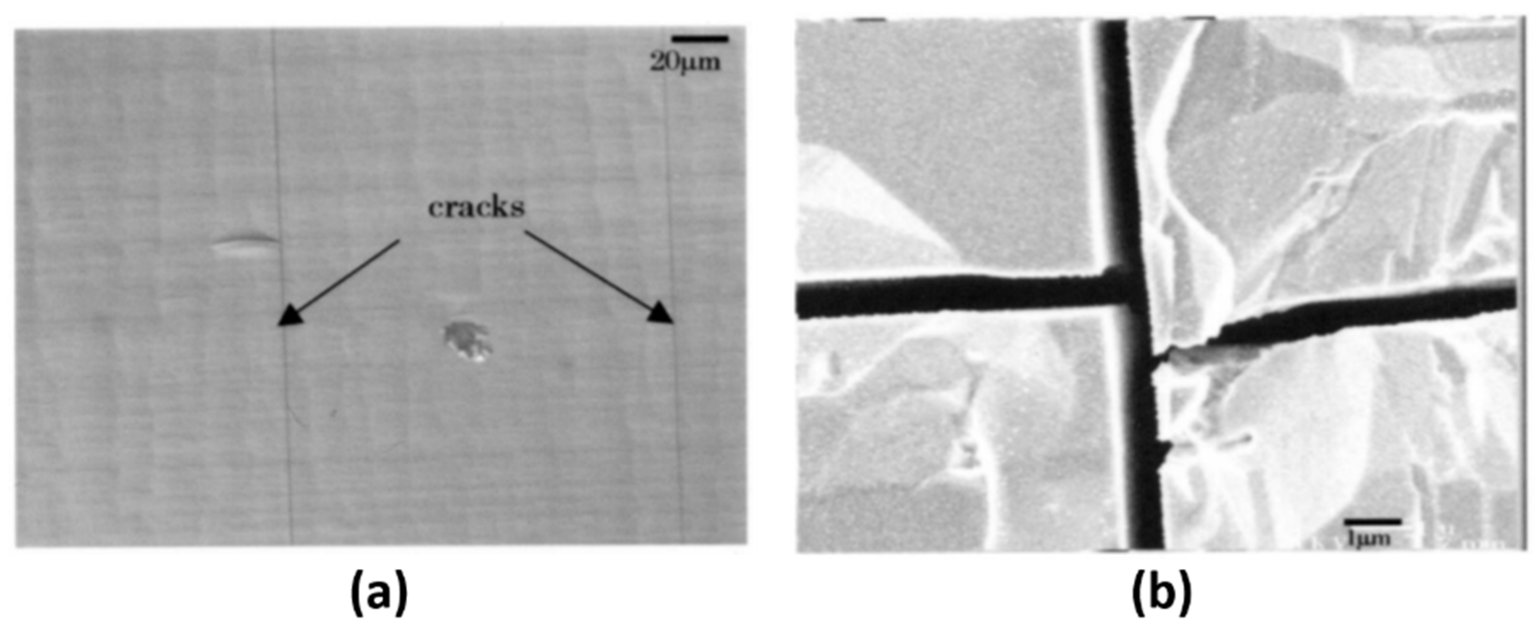
Second, the TDs originating from the large lattice mismatch between III-V and Si is also an important issue [28,76,77,78]. The lattice constant mismatch, e.g., 4% (8%) between GaAs (InP) and Si, introduces a build-up of strain energy on the epitaxial layer during the growth. If the thickness of III-V epilayer on Si exceeds a certain value, the so-called critical thickness, the accumulated strain energy proportional to the thickness of epilayer is released via the formation of misfit dislocations (MDs) along the heterointerface and TDs toward the surface. Matthews et al. [76] described a theoretical model for the critical thickness of epilayer. In this model, it is assumed that a pre-existing dislocation in substrate is replicated in the epitaxial layer and glides back and forth by the misfit strain to create misfit dislocation at the interface. The critical thickness h c is found to be
h c = b 2 π f ( 1 ν cos 2 α ) ( 1 + ν ) cos λ [ ln ( h c b ) + 1 ] ,
where b is the length of the Burgers vector for the dislocation, ν is the Poisson ratio, α is the angle between the dislocation line and its Burgers vector, f is the lattice mismatch strain, and λ is the angle between the slip plane and the line in the film plane that is perpendicular to the intersection line of the slip plane and interface.
As the line defects cannot be naturally terminated within the crystal lattice, the MDs along the heterointerface can reach the edge of epilayer or merge with pre-existing TDs within the substrate. In addition, the MDs can form the dislocation half-loop, introducing additional TDs which penetrate the whole layer and reach the surface. Because the dislocation half-loop is likely to be nucleated at pre-existing crystal defects, it is also important to control the crystal imperfection during the growth. It is well known that the TDs introduce the electronic state in the bandgap of III-V semiconductor which acts as nonradiative recombination centers.
The density of TDs is very important and straightforward parameter which describes the quality of epitaxial layer. There are three common approaches used to measure the TDD of III-V epitaxial layer [79,80,81]: (1) Etch-pit density (EPD) measurement; (2) Transmission electron microscopy (TEM) measurement; (3) X-ray diffraction (XRD) measurement. First, for EPD measurement, etching solution is applied to the semiconductors. Because the etching rate at the dislocation is higher than that at crystalline region, the pits around TDs are formed and thereby can be easily counted by optical observation or atomic force microscopy (AFM). The EPD measurement is very easy, quick, and cheap process, but it tends to underestimate the TDD. Moreover, quantitative analyses, such as Burgers vector determination, are impossible. Second, TEM measurement enables direct observation of TDs and quantitative analysis. However, an accurate analysis is restricted only to the highly defected crystals because of the small volume of the examined sample. Last, unlike the EPD and TEM measurements, XRD provides non-destructive measurement of TDD in the range from 105 to 109 cm−2. It is possible to calculate the TDD by measuring a few (hkl) rocking curve widths, because dislocations broaden the rocking curve. Gay et al. [82] and Ayers [81] introduced the theory for the measurement of TDD in metals and (001) zinc-blende semiconductors, respectively.

2.3. Thermal Crack

Finally, a large difference in coefficient of thermal expansion (CTE) causes the introduction of a thermal strain during any temperature changing process [83,84]. In particular, when the wafer cooled down from III-V growth temperature (580 °C for GaAs) to room temperature (RT), the accumulated thermal strain is likely to be relaxed by forming thermal cracks. The thermal cracks can be easily found in the GaAs-on-Si heteroepitaxy, where the GaAs has a larger CTE than Si (6.6 × 10⁻⁶ K−1 and 2.3 × 10⁻⁶ K−1 for GaAs and Si, respectively), because a tensile strain is applied to the epitaxial layer during the cool-down process. Griffith [85] first proposed the simple fracture model of brittle materials for predicting the onset of crack growth. In this model, the critical thickness of heteroepitaxial layer under tensile strain can be approximated. The derived condition for crack propagation is [86,87,88]
h G 2 γ π Υ ε 2 ,
where h G is the thickness of epitaxial layer, Υ is the biaxial modulus, γ is the surface energy per unit area for semiconductor, and ε is the in-plane tensile strain.
If the surface energy for the favorable (110) crack plane in zinc-blende structure is approximated by γ ( 110 ) = Υ ( 1 ν ) a / 2 2 π 2 , the Griffith criterion for crack propagation in the (001) heteroepitaxy of a zinc-blende semiconductor becomes [88]
h G a ( 1 ν ) 2 2 π 3 ε 2 ,
where a is the lattice constant, and ν is the Poisson ratio.
The Griffith criterion describes the condition for crack propagation, rather than for crack formation, under pre-existing cracks. Nonetheless, because the presence of any imperfections in the epitaxial layer also affects the crack formation [89], the thickness at which the crack forms may be close to the Griffith thickness h G [88]. A wide variety of theoretical models which describe the condition for crack formation can be found elsewhere [90,91].
In general, thermal crack lines exactly parallel or perpendicular to each other appear in the III-V epitaxial layer [92]. This can be explained by the unique <110> {111} slip system in zinc-blende III-V semiconductors. In case of zinc-blende III-V grown on (001) oriented substrates, most of misfit dislocations are 60° dislocations. Particularly, two types of misfit dislocations are preferred, α and β, lying along two orthogonal <110> directions at the interface, due to the asymmetry of zinc-blende crystal structure [93,94,95]. At the interface under tensile strain, the α (group V atom core) and β (group III atom core) dislocations have [ 110 ] and [ 1 ¯ 10 ] line direction, respectively. The directions of these dislocations are reversed at the interface under compressive stress. In addition, the asymmetric cracking occurs in III-V epitaxial layer, which means that the density of two orthogonal cracks is quite different [91,93,95,96]. During the early stage of crack formation, cracks with one of <110> directions are dominant. However, if the epitaxial layer is far thicker than the critical thickness of crack formation, orthogonal crack lines are commonly observed. This can be ascribed mainly to the difference in glide velocity of α and β dislocations [97].
In addition, as the crack nucleation originates from other pre-existing defects, the presence of any imperfections in the epitaxial layer also affects the crack formation [89]. Like other defects, the presence of thermal cracks introduces destructive effects on the quality of III-V epilayer and performance of optoelectronic devices, such as light scattering centers, electrical leakage path, and limitation on the total thickness of epilayer [98]. More importantly, like the APBs, high density of thermal cracks significantly reduces the yield of device fabrication.
For the GaAs-on-Si, thermal cracks begin to propagate if the thickness of GaAs exceeds about 3 μm, and the number of cracks increases as the thickness increases [89]. As shown in Figure 2a, the cracks appear predominantly in only one of <110> direction when the thickness of GaAs is close to the critical thickness for crack formation. For the thick GaAs (8.1 μm) layer far beyond critical thickness, high density of cracks in two orthogonal directions can be observed, as in Figure 2b.
For InP-on-Si, on the other hand, the issue of thermal cracks is not as critical as in GaAs-on-Si growth. It was reported that the thermally-induced tensile stress in InP film on Si was much less than that in GaAs film on Si [99]. This can be attributed to the fact that the InP has lower growth temperature and a smaller difference of CTE from Si, compared with GaAs. Additionally, the rearrangement of misfit dislocations in InP, partially accommodating the thermally-induced stress during the cooling process, occurs at relatively low temperature (~250 °C).

3. Approaches for High-Quality III-V on Silicon

3.1. APB-Free III-V on Silicon

To obtain a single domain of III-V materials on Si is prerequisite for growing high-quality III-V layer because the APBs, the planar defect, propagate from the heterointerface to the surface. Indeed, the presence of APBs makes it almost impossible to fabricate and operate optoelectronic devices. This section will introduce several methods to achieve APB-free III-V layer on Si substrates, mainly focusing on the use of on-axis (001) Si substrates. This is because most of modern ICs and PICs industry uses CMOS-compatible on-axis (001) Si substrates.

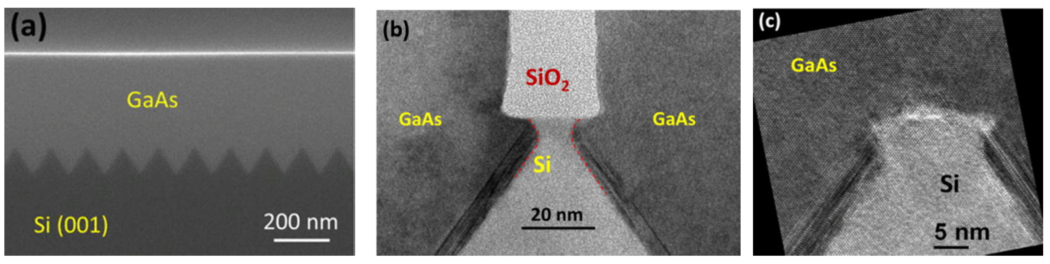
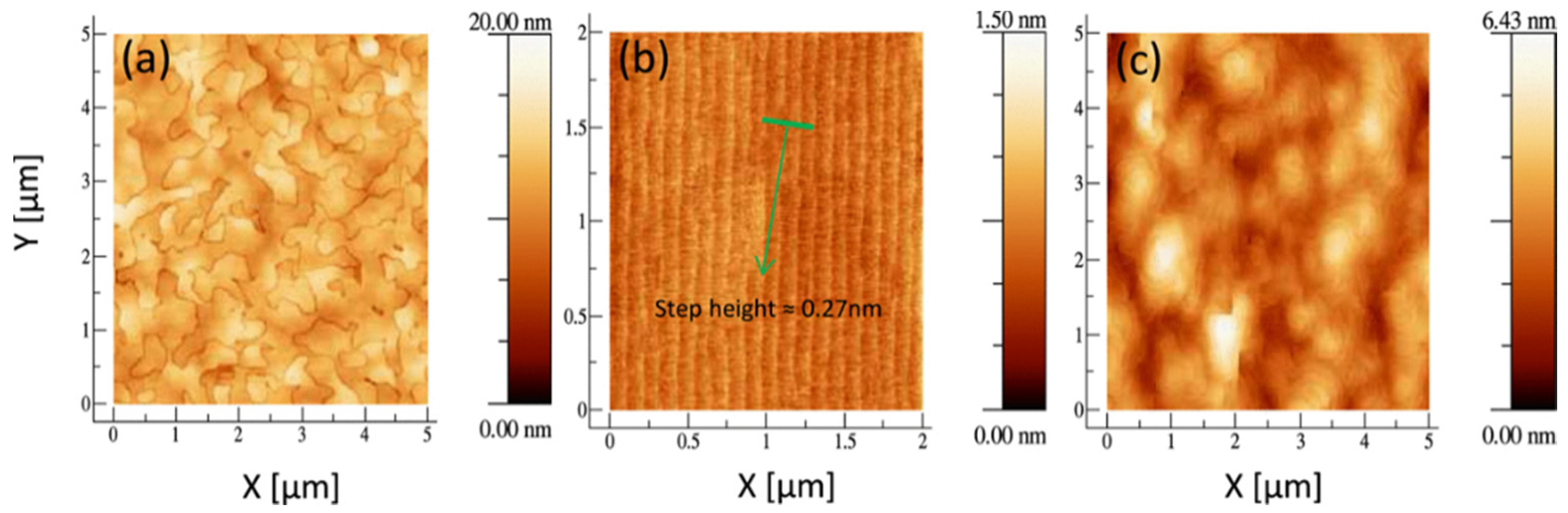
3.1.1. Offcut Silicon Substrates

It is well known that the use of offcut Si substrates with various angles from 4° to 7° is effective in suppression of the formation of APBs [100,101,102,103]. As mentioned in Section 2.1, the monatomic steps of the Si(001) surface consist of two alternating (2 × 1) and (1 × 2) dimerization. However, it was observed that the misoriented Si with an offcut angle larger than 4˚ experienced the surface reconstruction after proper annealing process, yielding a (2 × 1) single domain [73,74,104,105]. In this case, the Si-Si dimers are parallel to the upper terrace, and the steps are predominantly double-atomic steps. This reconstruction can be explained by the formation energy [74]. The monatomic steps are found to have lowest formation energy, but the formation of double-atomic steps is energetically preferred on the misoriented surface towards [ 110 ] or [ 1 ¯ 10 ] direction, in which the monatomic steps with dimers parallel and perpendicular to the upper terrace alternate. Therefore, the surface reconstruction in the offcut Si(001) is necessary to obtain the single domain of III-V layer on Si [106,107,108,109]. However, the formation of double-atomic step doesn’t always guarantee the APB-free III-V epitaxial layer on Si. Bringans et al. [110] reported the surface rearrangement of Si(001) by interaction with arsenic. On the double-atomic stepped Si(001) with a (2 × 1) single dimerization, applying As4 flux leads to the formation of a monolayer of As-As dimers, depending on the As4 flux exposure conditions. The orientation of As dimers can be parallel or perpendicular to the step edge, which can affect the nucleation of GaAs. To obtain the III-V single domain on Si, therefore, As or Ga pre-layer, as well as surface reconstruction, should be considered [111,112,113,114].
By using offcut Si substrates, high-quality III-V layers on Si without APBs have been successfully demonstrated [16,48,49]. However, the offcut Si substrates are incompatible with CMOS, as well as advanced Si manufacturing technologies. Moreover, recent booming development of Si photonics accelerates the necessity of CMOS-compatible on-axis (001) Si substrates. Unlike the offcut Si, it is very difficult to obtain the single domain of III-V on on-axis Si due to the difficulty in the reconstruction of monatomic steps, and therefore recent research focus of III-V-on-Si heteroepitaxy moved towards the growth of III-V on the CMOS-compatible on-axis (001) Si substrate.

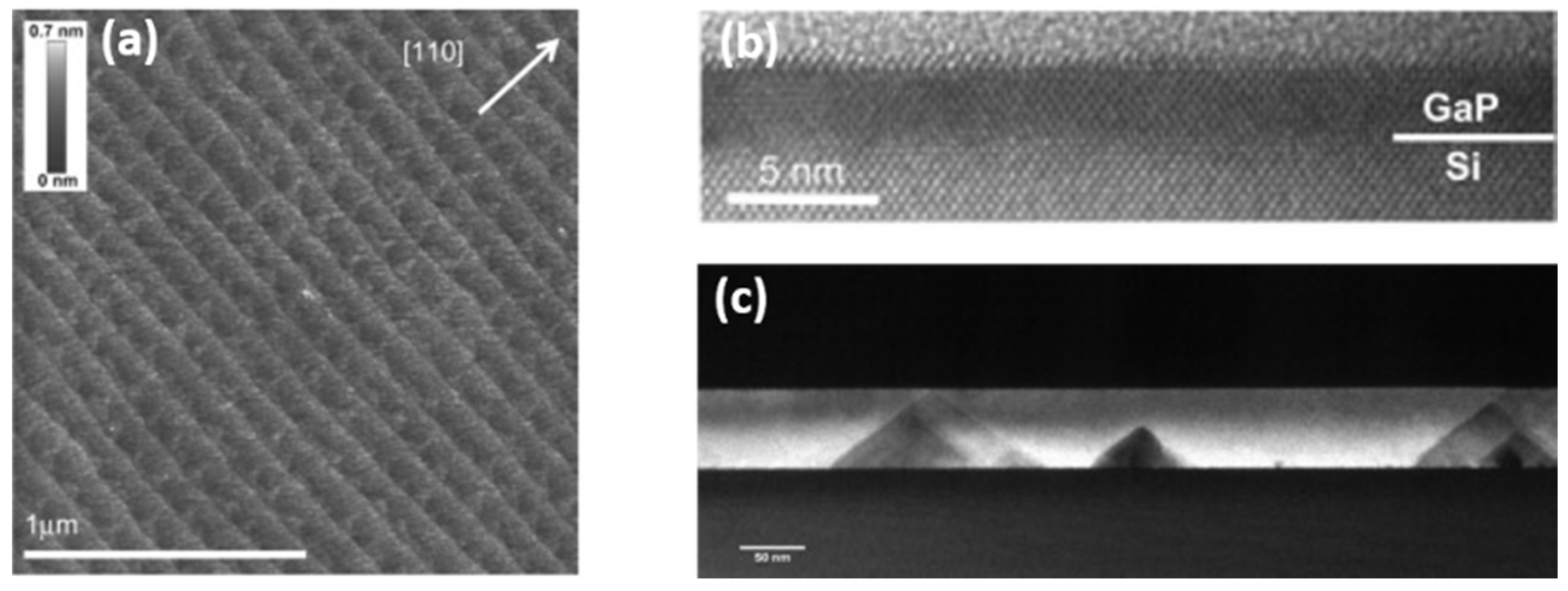
3.1.2. Selective Area Growth

The selective-area growth (SAG), allowing the epitaxial layer to grow on the pre-defined region, has been intensively developed due to its unique defect reduction property, the so-called aspect ratio trapping (ART) [115,116,117,118] or necking effect [119,120]. The basic concept of SAG is to trap the defects inside the sidewalls of patterned dielectric mask materials, typically SiO2, on Si substrates. Unlike the bulk growth, for the SAG technique, more complex growth parameters, as well as the optimization of mask pattern design, are required to achieve high-quality selective growth because of the reduced dimensions and confined structures [26]. Nonetheless, the SAG is very effective in reducing the density of defects if the dielectric mask pattern has enough aspect ratio (h/w where h and w indicate mask height and width, respectively). As shown in Figure 3, the TD segments are likely to glide along the { 111 } slip plane, which forms an angle of 54.7° with the 110 orientation during the growth. Hence, the TD segments on the { 111 } slip plane, reaching the oxide sidewall, are trapped, regardless of whether the { 111 } slip plane is parallel or perpendicular to the trench orientation. In addition, the angle of 54.7° determines the minimum aspect ratio (at least 1.43) for trapping the TDs on the { 111 } slip plane. The SAG using trench structures also traps the planar defects, namely the APBs, in a similar way of TDs. However, only planar defects formed on the { 111 } plane parallel to the trench orientation can be trapped, as shown in the third case of Figure 3. In other words, the planar defects on planes perpendicular to the trench orientation will not be trapped. However, Orzali et al. [121], who employed the chemically etched V-shaped Si surface for defect reduction, reported that the nucleation of GaAs initiated only on the etched {111} Si plane contributed to the prevention of APB formation.
Even though many SAG techniques have shown their capability of reducing the density of defects, the APB issue is not fully resolved. In order to address APB and rough surface issues, growing III-V materials on the chemically etched (111) Si surface with nanowire coalescence was proposed [122,123]. For example, Li et al. [123] reported GaAs-on-V-grooved Si (GoVS) templates which offered APB-free flat GaAs layer on on-axis (001) Si substrates. To obtain GoVS template, n-type on-axis (001) Si substrates patterned with SiO2 stripe were chemically etched by potassium hydroxide (KOH) solution to form trench structure exposing (111) facets, and subsequently the GaAs nanowires were selectively grown on the V-grooved Si by metal-organic chemical vapor deposition (MOCVD). After removing the SiO2 stripe pattern, coalesced GaAs thin films were regrown on the nanowire arrays. Figure 4a shows a scanning electron microscopy (SEM) image of the resultant coalesced GaAs layer with a flat surface. The surface morphology of 300 nm-thick coalesced GaAs layer measured by atomic-force microscopy (AFM) produced a root-mean-square (rms) of 1.9 nm across a scanned area of 5 × 5 μm2. The APBs were not observed in the GoVS template, which can be explained by the III-V growth on Si {111} plane. A transmission electron microscopy (TEM) image in Figure 4b presents a unique stacking fault trapping. It was shown that a tiara-like structure beneath the SiO2 sidewall, created by Si undercutting, effectively trapped most of the stacking faults around the interface of GaAs/Si(111). Owing to this unique trapping mechanism, after removing the SiO2, the subsequent GaAs overgrowth can be performed with maintaining the ability of defect trapping, as shown in Figure 4c. Although some of stacking faults can escape the tiara-like structure in the thick stacking-disorder regions, the escaped stacking faults can be annihilated by crossing of two stacking faults due to the closely spaced V-groove structure.
For the InP growth on on-axis Si, Zhu et al. [124], investigating the APB-free InP-on-grooved Si (IoVS) templates similar to the GoVS, demonstrated electrically pumped 1.5-μm InGaAs/InAlGaAs laser monolithically grown on IoVS template. The method for obtaining IoVS template is very similar to that of GoVS. A main difference is that a 10 nm-thick GaAs wetting layer was grown on the exposed (111) Si facets before the InP nanowire growth. This is because employing GaAs wetting layer reduces a strain for InP growth and prevents InP seed layer from being clustered.

3.1.3. MOCVD/MOVPE-Grown Buffer Layer

Alcotte et al. [125] developed APB-free GaAs layer directly grown on nominal (001) Si substrates without the SAG. In this work, microelectronics standard nominal (001) Si 300 mm wafers, first deoxidized in a SiConiTM chamber with NF3/NH3 remote plasma, were subsequently transferred into the MOCVD chamber and annealed at high temperature (800 °C~950 °C) in H2 ambient. This optimized preparation promotes reconstructing the 2 × 1 surface, namely the formation of double atomic steps, which is believed to be a crucial step for inhibiting the formation of APBs. In Figure 5a, the AFM image of a 400 nm-thick GaAs grown on unoptimized Si shows a high density of randomly distributed APBs. In contrast, the optimized Si surface mainly consists of double atomic steps (Figure 5b), and the APBs were not observed in the 150 nm-thick GaAs layer grown on optimized Si (Figure 5c). In addition, the surface roughness of 150 nm GaAs layer grown on optimized Si was measured to be 0.8 nm rms, corresponding to the lowest value reported for 1 μm-thick GaAs grown on offcut Si substrates.
In addition to the GaAs/Si, Volz et al. [126] also demonstrated the APB-free GaP/Si template using homoepitaxial Si buffer and heteroepitaxial GaP buffer layer grown by vapor phase epitaxy (VPE) and metal-organic vapor phase epitaxy (MOVPE), respectively. To obtain APB-free GaP/Si template, the 500 nm-thick homoepitaxial Si buffer layer was first grown on deoxidized on-axis (001) Si at 200 mbar and 850 °C, where the optimized post-annealing (10 min, 950 mbar H2, 975 °C) process was subsequently performed. In Figure 6a, the AFM image of the annealed Si buffer surface confirms the formation of double-atomic steps (0.27 nm height), which is believed to be responsible for preventing APB nucleation. Then, the GaP layer was grown on the prepared Si buffer layer in a two-step procedure consisting of a nucleation and an overgrowth. For the optimal growth of GaP nucleation layer, flow-rate modulated epitaxy (FME) method, in which the Ga and P precursors are alternately injected into reactor, was employed. The low-temperature FME growth mode results in a two-dimensional continuous GaP nucleation layer, irrespective of whether Ga or P was first deposited. Figure 6b presents a TEM image of a continuous GaP nucleation layer grown by P-started FME method at 450 °C. In contrast, a continuously-injected nucleation forms three-dimensional GaP islands, which can evolve into stacking faults upon coalescence. After the growth of the optimal 3 nm GaP nucleation layer, bulk GaP layer was overgrown at 625 °C with continuous growth mode. As shown in Figure 6c, most of APBs are self-annihilated within 50 nm-thick GaP layers by kinking towards {111} plane or higher index plane. Consequently, the formation of double-atomic steps by the annealed homoepitaxial Si buffer contributed to the suppression of APB nucleation, and the two-step GaP growth on the Si buffer consisting of low-temperature (LT) FME nucleation and high-temperature HT overgrowth enabled APBs to kink and self-annihilate with each other.

3.1.4. MBE-Grown Buffer Layer

Most of the mature approaches for APB elimination employ MOCVD/MOVPE growth system to obtain virtual templates, such as GoVS, GaAs/Si, and GaP/Si. In general, these methods require pre-treatment under high temperature and high-pressure hydrogen before growth to promote the formation of double-atomic steps. On the other hand, solid-state molecular beam epitaxy (MBE) doesn’t provide the hydrogen-based treatment. Nonetheless, all MBE-grown and APB-free III-V layer on on-axis Si is beneficial in terms of the low-cost and straightforward process because III-V devices grown on GaP/Si or GaAs/Si virtual substrates commonly use two different growth system, namely III-V and APB-free buffer growth by MBE and MOCVD/MOVPE, respectively. In addition, the MBE system has shown superior performance in growing high-quality InAs/GaAs QD lasers, which are promising Si-based light sources in Si photonics.
There have been only a few reports on the approaches using direct MBE growth without a virtual template. For example, Kwoen et al. [127], investigating the effect of AlGaAs nucleation layer on the elimination of APBs, demonstrated APB-free GaAs layer directly grown on on-axis (001) Si. In this paper, four different compositions of 40 nm-thick AlxGa1-xAs nucleation layer was investigated, and subsequently 2.3 μm-thick GaAs buffer layer was grown. Figure 7a–d present the cross-sectional SEM images of GaAs/Si with AlxGa1−xAs and GaAs nucleation layer. Unlike the GaAs/Si with Al0.7Ga0.3As seed layer in which APBs extended to GaAs surface (Figure 7d), the Al0.3Ga0.7As seed layer was effective in self-annihilation of APBs near the nucleation layer (Figure 7b). The GaAs crystal quality was also confirmed by photoluminescence (PL) emission intensity. As shown in Figure 7e, the PL intensity of InAs QD layer grown on GaAs/Si with Al0.3Ga0.7As nucleation layer was two times higher than that with a GaAs nucleation layer, and, as the Al content of AlxGa1−xAs nucleation layer increases, the PL intensity tended to decrease. It was revealed that the APB-free GaAs layer could be obtained by employing the Al0.3Ga0.7As nucleation layer and the APB suppression mechanism was attributed to the self-annihilation of APBs rather than the formation of double-atomic step on Si surface. However, the detailed annihilation mechanism is not clearly understood, and the critical growth parameters remain uncertain.
It was previously believed that the formation of double-atomic (D) steps on Si was the key step for APB or IB annihilation during the III-V growth on Si. In 2020, however, Li et al. [128] first proposed a new mechanism for APB annihilation and reported all MBE-grown APB-free GaAs monolithically grown on on-axis Si (001) using an annealed Si buffer layer. In this report, a 200 nm-thick Si buffer layer, comprised of 100 nm-thick Si layer and five sets of 20 nm-thick Si layers annealed at 900 °C and 1200 °C, respectively, was grown on the deoxidized on-axis (001) Si substrate. Subsequently, conventional GaAs buffer layer, defect filter layers (DFLs), and QD laser structures were grown. Both the use of AlGaAs seed layer [127,129] and heat treatment on the deoxidized Si (001) substrate up to 1200 °C [130], known to offer APB-free GaAs growth on Si, showed APBs on the GaAs surface in this experiment, whereas the sample with an annealed 200 nm-thick Si buffer layer exhibited APB-free GaAs surface. To examine the origin of the APB annihilation, AFM images of surface morphology of Si substrates without and with the annealed Si buffer layer were shown in Figure 8a,b, respectively. Contrary to the deoxidized Si surface showing a random atomic-step distribution (Figure 8a), ordered Si steps were observed in the annealed buffer Si surface, as shown in Figure 8b. The ordered Si steps consist of alternating straight and meandering Si monatomic steps (Figure 8c), each of which has the height of around 0.13 nm (Figure 8d). This indicates that the annealed Si buffer produces single-atomic (S) steps rather than the D steps. The inset of Figure 8c illustrates a schematic diagram of alternating straight and meandering single-atomic steps denoted by Sa and Sb, respectively.
Cross-sectional TEM measurements with two viewing directions of [ 110 ] (Figure 9a–d) and [ 1 1 ¯ 0 ] (Figure 9e,f) were conducted on the sample without and with the annealed Si buffer layer. For the sample without the annealed Si buffer, although the APBs nucleated at the GaAs/Si interface propagate along higher index planes and hence annihilate with each other (Figure 9a), some APBs which are not self-annihilated penetrate the whole GaAs layer (Figure 9c). For the sample with the annealed Si buffer, on the other hand, periodic arrays of the self-annihilated APBs, where the distance between the periodic arrays corresponds to the half-width of each Si step terrace, were observed in Figure 9b. Moreover, most of the APBs initiated from Sa + Sb array were annihilated within 500 nm-thick GaAs layer, as shown in Figure 9d. A similar tendency was also confirmed from [ 1 1 ¯ 0 ] direction view in Figure 9e,f. Consequently, it was revealed for the first time that the Si surface with alternating straight Sa and meandering Sb single-atomic steps, formed by the annealed Si buffer layer, enabled the periodic APBs to follow the shapes of Sa + Sb steps and annihilate within 500 nm-thick GaAs overlayer.

3.2. Reduction of the Dislocations

For high-quality III-V layer monolithically grown on Si, achieving a low density of TD is a key issue. In particular, the TDs penetrating an active region of optoelectronic devices significantly degrade their performance. For example, quantum-well (QW) lasers monolithically grown on Si substrates, in which the TDD is 5 × 107 cm−2 corresponding to common TDD of GaAs/Si, shows no lasing behavior [131]. Therefore, a great deal of effort has been made on the reduction of TDD since the 1980s, and now the TDD of about 106 cm−2 for GaAs-on-Si can be achieved [48,132]. This section introduces general approaches essential for reducing TDD in III-V/Si heteroepitaxy.

3.2.1. Nucleation and III-V Buffer Layer

Initial stage of III-V growth on Si plays an important role since the growth begins with the formation of the island on Si surface, which considerably affects the TDD of the following overlayer. Therefore, a wide variety of methods have been extensively studied, including Si buffer layer [133,134], pre-layer formation [112,135,136], two-step growth [106,108], migration-enhanced epitaxy [137,138], and amorphous buffer layer [139,140]. Among these approaches, the so-called two-step growth has been most widely adopted in GaAs/Si. The two-step growth starts with low-temperature (LT) growth (400 °C) of GaAs in the initial stage, followed by annealing and growing the GaAs at typical growth temperature about 550 °C~600 °C. The reason for using this growth order is because at LT the GaAs becomes continuous before the defects are introduced. Figure 10 compares the ways how the GaAs islands coalesce into a continuous layer at high and low growth temperature [25]. At the typical growth temperature of GaAs (550 °C~600 °C), the GaAs islands have a lot of defects before coalesced. Once these islands coalesce, the defects, trapped inside the island, are extended in continuous layer. Then, the extended defects are difficult to be removed. In general, LT growth introduces a higher density of islands than that of high-temperature (HT) growth due to the reduced diffusive mobility of adatoms. For LT growth, therefore, many defects originating from the high density of islands are generated. Hence, two-step growth including LT growth is expected to produce high density of defects. However, the two-step growth generally exhibits much better structural properties than single-step growth. This can be explained by that the defects of which the form is less diverse and more mobile may annihilate during growth and coalescing.
In addition, a three-step growth, the modified two-step growth method in which an intermediate-temperature (IT) layer is added between LT and HT layer, was commonly employed in recent years [128,141,142,143]. Nozaki et al. [144] proposed and reported that the three-step growth method in GaAs-on-Si improved the surface morphology, as well as crystallinity. The detailed mechanism of this improvement was not clearly understood, but it was ascribed to the GaAs top layer grown at HT without direct contact to the LT nucleation layer. In addition, Wang et al. [145] directly compared the effect of three-step growth on the quality of GaAs on Si with two-step growth. It was shown that the three-step growth with two thermal cycle annealing produced rms roughness of 1.8 nm and the TDD of 1.1 × 107 cm−2 (3 × 106 cm−2) calculated from XRD (EPD), all of which are improved compared with the conventional two-step process.
Similar to GaAs/Si, the InP-on-Si system also commonly employs the two-step growth [146,147,148]. However, direct growth of InP on Si produces much higher TDD than that of GaAs on Si due to larger lattice mismatch (~8%) [149]. For the InP-on-Si, accordingly, the insertion of the intermediate buffer layer between InP and Si is preferred.

3.2.2. Intermediate Buffer Layer

To avoid the problem arising from material dissimilarity between Si and III-V, the basic solution to insert other materials of which the lattice constant and CTE are matched with Si has been developed. For GaAs/Si heteroepitaxy, a wide variety of methods using germanium (Ge) [150,151,152,153,154], GaAsP [155,156], and InGaP [157] were developed. Among these materials, Ge has been most widely used because of its complete miscibility with Si, well-developed Ge-on-Si growth technology, and nearly the same lattice constant and CTE matching between GaAs and Ge [158]. Moreover, the compositionally graded Ge/GexSi1−x offers efficient strain relaxation in the buffer layer, and therefore a final Ge cap layer serves as a virtual substrate for GaAs growth. In 1991, Fitzgerald et al. [159] reported the primary study on the compositionally graded GexSi1−x layers (x = 0.23, 0.32, and 0.5) on Si, producing the TDD on the order of low 106 cm−2. After that, substantial efforts have been devoted to achieving an artificial Ge/GexSi1−x/Si substrates [113,160,161,162,163,164]. For instance, Groenert et al. [158] demonstrated RT continuous-wave (cw) GaAs/AlxGa1−xAs QW lasers monolithically grown on the graded Ge/GexSi1−x/Si virtual substrates. As shown in Figure 11, most of dislocations are effectively confined within graded GexSi1−x buffer layer, which offers strain relaxed pure Ge top layer and GaAs layer. The TDD on the Ge cap layer was measured to be 1.2 × 106 cm−2.
Today, for GaAs/Si system, direct growth of GaAs buffer layers using multi-step growth method is more preferred to the intermediate buffer layer, such as Ge or graded GeSi layers. This is because the use of Ge/GeSi buffer generally requires much thicker layers than that of common GaAs buffer layers despite similar TDD on the order of low 106 cm−2. For the monolithic integration on Si platform, in general, a thin buffer layer is favorable in terms of thermal cracks [98] and co-integration with other components [12]. Although using thin Ge/GeSi buffer layers has been also demonstrated [165], the order of TDD (~108 cm−2) is much higher than that of thick Ge/GeSi or GaAs buffer layer (~106 cm−2). In addition, the chemical-mechanical polishing (CMP) process [164] used to obtain smooth surface in rough Ge/GeSi buffers can increase the fabrication cost and complexity.
Unlike the GaAs/Si, the InP/Si heteroepitaxy normally adopts the intermediate (graded) buffer layers because of the large lattice mismatch between InP and Si (~8%). The prevailing material commonly used for the intermediate buffer is GaAs [166,167,168,169]. The most typical approach for growing InP on Si is employing the mature multi-step growth of GaAs on Si with strained-layer superlattices filtering the TDs [149,170,171]. Even though the GaP buffer layer has also been utilized, it was known to be less effective in terms of TDD, residual stress, and quality of InP, compared with the GaAs buffer layer [172,173,174]. Besides, the employment of compositionally graded buffer layer, including InGaAs, InGaP, InAlAs, and InGaAlAs alloys, has shown successful reduction of the TDD in InP/GaAs [175,176,177,178]. For example, Quitoriano et al. [175], who studied graded buffers grown on GaAs substrates to obtain high-quality InP without phase separation, demonstrated low TDD of 1.2 × 106 cm-2 through the hybrid InGaAs and InGaP graded buffer layer. In a similar way, to further decrease the TDD of InP/GaAs/Si epitaxy, growing the graded buffer layers on the GaAs/Si substrates has also been explored. For instance, Shi et al. [149] have shown a low TDD of 5 × 106 cm−2 by using 1.8 μm-thick graded In0.4Ga0.6As buffers on 2 μm-thick GoVS template.

3.2.3. Epitaxial Lateral Overgrowth

Epitaxial lateral overgrowth (ELO) is also an important technique to inhibit the propagation of TDs in epitaxial layer. Like ART process reviewed in Section 3.1.2, ELO is also based on SAG method. In the ELO process, a III-V buffer layer is first grown on Si substrate, and subsequently a dielectric mask, such as SiO2, is deposited on the III-V buffer layer. Then, the dielectric mask is selectively etched to expose the III-V buffer layer for regrowth. Then, the III-V epitaxial layer is vertically regrown through the opened region of the mask and thereafter can be laterally grown over the mask. The most of TDs in the buffer layer are blocked by the bottom of the mask, but a small number of TDs around the opened region will propagate upwards, as shown in Figure 12a. Therefore, the laterally grown epitaxial layer above the dielectric mask exhibits a high crystalline quality.
For the GaAs on Si, pioneering works on ELO have been reported since 1980s [180,181,182]. However, the early reports on ELO for GaAs-on-Si suffered from the limited defect-free region and the mechanical weakness of the laterally grown parts, both of which became severe as the ELO layer was further grown. In order to resolve these limitations of ELO technique, a great deal of effort has been dedicated to optimizing growth conditions [118,179,183,184,185,186,187,188,189]. For example, Chang et al. [179], investigating the dependence of the ratio of the ELO layer width to the thickness (W/T ratio) on the growth temperature and the seed line separation, showed that the width of dislocation-free GaAs region achieved about 43 μm. In this work, misoriented (100) Si substrates, on which a GaAs buffer layer was grown by MBE, were used for ELO of GaAs by liquid phase epitaxy (LPE). For comparison, the width of the line seed (opened region for regrowth) was fixed as 5 μm, but the line seed separation was varied as 200, 500, and 1000 μm. In addition, growth temperature of GaAs was chosen as 500, 530, and 560 °C. As shown in Figure 12b, a maximum W/T ratio of 17.5 was achieved by the line seed separation of 500 μm and the growth temperature of 530 °C. Figure 12c shows a wide ELO layers of 195 μm-width after the growth time of 7 hours. To identify dislocation-free region, etch-pit density (EPD) was measured by KOH etching. As shown in Figure 12d, a high density of TDs which propagated from the GaAs buffer layer through the narrow line seed region can be clearly seen. However, no etch pits were found in the laterally overgrown GaAs. In addition, He et al. [188] proposed a three-stage ELO to obtain uniform and flat coalescence of selectively grown GaAs. In this report, 1.8 μm GaAs buffer was first grown on 4° offcut (001) Si substrate toward the <011> direction. Then, 80 nm-thick SiO2 mask was deposited on buffer layer, and nano-trench of 120 nm-width and 100 nm-separation was patterned on the mask. Last, the three-stage of ELO growth, comprised of the selective growth, coalescence, and planar growth stage, were carried out by MOCVD. It was shown that the nano-trench and three-step growth resulted in a mirror-smooth coalesced 410 nm-thick GaAs film.
In case of InP-on-Si, ELO techniques have been more widely employed [190,191,192,193,194,195,196], compared with GaAs-on-Si in which direct growth of GaAs on Si is preferred. Because it is very difficult to obtain low density of TDs through the direct growth of InP on Si, the use of ELO method is beneficial for achieving high-quality InP layer on Si. For the optimization of parameters of InP ELO on (001) InP substrate, Sun et al. [197] investigated the dependence of lateral overgrowth and vertical growth rate of InP on the mask stripe orientation. It was revealed that while the vertical growth rate was relatively independent of the opened stripe orientation, the maximum lateral overgrowth rate was achieved when the opened stripe oriented at 30° and 60° off [110] direction, as shown in Figure 13a. Following this result, Sun et al. [198] achieved a broad lateral overgrowth of InP on (001) Si substrate. In addition, Metaferia et al. [199] studied the morphological evolution during ELO of InP on Si with mesh opening, and showed that the coalesced region produced the TDD in a range from 6 × 106 cm−2 to 4 × 107 cm−2 depending on the thickness of ELO layer. In this work, 1.5 μm-thick InP/Si and 40 nm-thick SiO2 mask were used to overgrow InP. The mesh and line masks (opening and masking width of 200 nm and 3 μm, respectively), tilted 15° and 30° off the [110] direction, are compared. The angle between the opening line in mask and [110] direction was chosen from previous result by Sun et al. [197]. As shown in Figure 13b,c, the coalescence of the InP layer occurs predominantly at the corners of the mask. Such a coalescence mechanism in mesh mask resulted in higher growth rate than that in line mask, attributed to the less probability of the boundary plane formation. The quicker coalescence in the mesh opening resulted in better surface roughness at the early growth stage (~10 μm-thick InP layer), but, after an extended growth (~100 μm-thick InP layer), both mesh and line opening cases exhibited a similar surface roughness (rms roughness of 16 nm~25 nm). It was shown that regardless of both angles (15° and 30°) and masks (mesh and line opening) the TDDs were measured to be similar value. The TDD of about 10 μm-thick and 100 μm-thick InP layer was measured to be 2~4 × 107 cm−2 and 6~7 × 106 cm−2, respectively.

3.2.4. Thermal Annealing

The traditional way to reduce defect density is thermal cycle annealing (TCA) during growth, enabling thermally-activated dislocation migration and thus the annihilation of dislocations. Indeed, the TCA-induced reduction of TDD in GaAs/Si has been substantially investigated [200,201,202,203,204,205]. For instance, Yamaguchi et al. [201], investigating the TCA effects on the defect reduction in GaAs/Si, reported that the dislocation density was considerably reduced as the annealing temperature and cycling number increased. The etch pit density (EPD) was reduced from 108 cm−2 to 2 × 106 cm−2 after TCA. It was revealed that the thermally-induced stress as a driving force of dislocation motion contributed to the dislocation annihilation, such as coalescence. The numerical analysis also showed that the large number of TCA and/or annealing temperatures of more than 700 °C were effective in the reduction of TDD. However, in the case that the grown films initially have low density of dislocation which can move and coalesce, the attainable reduction of TDD is limited. In addition, Jung et al. [203] demonstrated that the in-situ TCA effectively reduced the TDD of GaAs grown on on-axis GaP/Si (001). To investigate the effect of in-situ TCA, a 1.5 μm-thick GaAs layer was first grown on GaP/Si, followed by four cycles of annealing. Then, another 1.5 μm-thick GaAs layer was regrown. For comparison, 3 μm-thick GaAs layer was also grown on GaP/Si without TCA. During in-situ TCA, the wafer was heated up to 700 °C and held for 5 min. Then, the temperature cooled down to 320 °C. The electron channeling contrast imaging (ECCI) revealed that the TDD of the TCA-treated sample (5.5 × 107 cm−2) was much lower than that of untreated sample (2.8 × 108 cm−2). It was also found that the TCA process improved the surface roughness from 7.8 nm to 4.8 nm (rms). Recently, Shang et al. [206] investigated the effect of TCA on the reduction in TDD of GaAs-on-Si template. As shown in Figure 14A, a minimum TDD of 3 × 107 cm−2 was obtained after 12 cycles of TCA. A noticeable reduction in TDD was achieved at 4 (8) cycles of annealing at 735 °C (700 °C). The maximum annealing temperature was set to below 745 °C because annealing at above 745 ˚C causes remarkable degradation of the GaAs surface, such as the formation of Ga droplet, as shown in Figure 14B. In Figure 14C, ECCI images showed that the TDD was reduced from 4.18 × 108 cm−2 to 3 × 107 cm−2 after 16 cycles of TCA. It should be noted that a surface TDD lower than 2 × 106 cm-2 was obtained after a step-graded filter layer was grown on the post-TCA GaAs-on-Si. In a similar mechanism of TCA, post-growth annealing (PGA), carried out after completing the growth, has also been widely employed to reduce the TDD of GaAs [207,208,209].
For the InP/Si, TCA or PGA has also been applied to improve the crystal quality [168,169,210,211]. However, the effect of thermal annealing on the defect reduction is not as dramatic as in GaAs/Si because the difference of CTE between InP and Si is relatively small; thus, the dislocation motion by thermally-driven stress is limited.

3.2.5. Strained-Layer Superlattices Defect Filter Layer

Strained-layer superlattices (SLSs) have long been extensively investigated in order to reduce the dislocation density since the 1980s [212,213,214,215]. Matthews et al. [212], who proposed the use of an SLS to reduce the TDD, demonstrated that the strain field in GaAsP-GaAs superlattice turned aside the TD propagating upward. The SLSs commonly consist of multiple pairs of two lattice-mismatched layers alternately under compression and tension. If the thickness of each SLS layer is less than a certain critical thickness, which otherwise creates misfit dislocations, each SLS layer accommodates elastic strains caused by lattice mismatch. The strain field of SLSs can bend over and force the dislocations propagating upward to move laterally toward the edge of the sample, leading to the dislocation coalescence and annihilation. Noted that the SLSs should have enough lattice mismatch and thickness to generate strain required for bending dislocations.
Ternary-binary SLSs DFLs have been widely used in GaAs/Si heteroepitaxy, including InGaAs/GaAs, InAlAs/GaAs, GaAsP/GaAs, and so on [216,217,218,219,220,221,222,223,224]. For example, Mingchu et al. [224] optimized InGaAs/GaAs DFLs for 1.3-μm QD lasers on Si. In this work, the indium composition and thickness in InxGa1−xAs/GaAs SLSs, as well as the growth condition of GaAs spacer layer, were investigated. In the growth method I (Figure 15a), the GaAs spacer layer was grown while the temperature in chamber was ramping up from 420 °C to 610 °C after the SLS growth at 420 °C. In contrast, in the growth method II (Figure 15b), the GaAs spacer layer was grown at 610 °C after finishing the ramp-up of temperature and in-situ annealing of the SLSs. In Figure 15c, the PL peak intensity of QD laser structure with growth method II was at least three times higher than that with growth method I. This improvement can be attributed to the high-temperature growth of GaAs spacer layer and in-situ annealing of SLSs. The high-temperature growth and annealing promoted the dislocation motion and resultant annihilation. It is also revealed that the optimized indium composition and GaAs thickness in SLSs were 0.18 and 10 nm, respectively. In Figure 15d, it was shown that the employment of three sets of In0.18Ga0.82As/GaAs SLSs DFLs effectively blocked and annihilated the TDs.
In the InP/Si platform, the DFLs based on InGaAs/InP, In(Ga)AsP/InP, (In)GaP/InP, and so on [149,170,225,226,227,228,229,230] have been also commonly adopted. For instance, Shi et al. [149] reported the effect of In0.73Ga0.27As/InP SLSs DFLs on the reduction of TDD in InP grown on on-axis (001) Si. In this report, InP buffer layers were first grown on GoVS template using multi-step growth, followed by four sets of InGaAs (13 nm)/InP (19 nm) 10-pair SLSs with 300 nm-thick InP spacer layers. In Figure 16a, bright-field scanning transmission electron microscopy (STEM) image of InP-on-Si structure exhibits the generation and propagation of TDs. A high density of TDs on the order of 1010 cm−2 generated from the InP/GaAs interface (line 1) was reduced to the TDD of 1.5 × 109 cm−2 through multi-step grown InP buffer layer (line 2). The final InP surface defect density was measured to be 1.17 × 108 cm−2 after four sets of InGaAs/InP DFLs (line 6). In Figure 16b, a zoomed-in STEM image of SLSs DFLs clearly shows that most of the dislocations are bent along the bottom or top interfaces of each SLS layer, resulting in the mutual annihilation of TDs. It was also revealed that SLSs with high indium composition (In0.82Ga0.18As) achieved low TDD of 7.9 × 107 cm−2 but formed rough surface with many hillocks. By considering surface morphology, as well as defect filtering efficiency, therefore, the optimized indium composition was about 71%. However, in general, using SLSs DFLs in InP-on-Si is not as effective as in GaAs-on-Si. For example, the TDD of InP-based materials remains on the order of 108 cm−2, while, in GaAs-based materials, the order of 106 cm−2 can be achieved. The reason for the discrepancy is not clearly understood, but it is believed to be due to the phase separation in the SLSs and/or the high density of dislocations arising from larger lattice mismatch in InP/Si than that in GaAs/Si [175]. It is also reported that, if the TDD is on the order of 108 cm−2 or greater, the SLSs is not very effective in dislocation filtering [216].
In addition, instead of SLSs, the self-assembled QDs can be used as DFLs [231,232,233]. The employment of InAs QDs as DFLs in GaAs-based material was first proposed and demonstrated by Yang et al. [231]. Because the strain-driven self-organized QDs produce large three-dimensional strain field around themselves, dislocations around QDs can be bent over and annihilated in a similar way to SLSs DFLs. For instance, Shi et al. [232] reported a four-fold reduction in density of TDs in InP/Si system by using self-organized InAs/InAlGaAs QDs as DFLs. In Figure 17a, a number of TDs, generated from InP/GaAs and GaAs/Si interfaces, propagate toward the top surface, leading to the TDD of 1.3 × 109 cm−2. In contrast, adopting the seven-layer of InAs/InAlGaAs QDs DFLs in InP/Si clearly shows dislocation bending and filtering effects, offering a four-fold reduction in TDD (3.2 × 108 cm−2), as shown in Figure 17b.

3.3. Minimizing Thermal Cracks

Controlling thermally-induced strain during the growth is very important because the residual strain by a large difference of CTE leads to thermal cracks or delamination, which are unacceptable for the device fabrication. In order to prevent the crack formation, basically, the thickness of epitaxial layer should be less than the critical thickness of crack formation. In addition, any imperfections, such as surface contaminants and defects, should be minimized because the formation of thermal crack is heterogeneous nucleation [98]. For III-V-on-Si heteroepitaxy, however, both thick buffer layers and crystal imperfections are inevitable. Therefore, various strategies for minimizing thermal cracks, including porous Si layer [234], strain compensated layer [235,236], use of indium dopant [237], and patterned substrate [83,92,238,239], have been proposed. Among these techniques, the use of patterning has been widely developed. For example, Huang et al. [239] reported crack-free GaAs layer on Si with an area of 800 × 700 μm2 by employing mid-patterned growth. In this work, to obtain crack-free GaAs/Si template, three steps were carried out: (1) a 2.3 μm-thick GaAs layer with AlAs/AlGaAs nucleation layer was first grown on (100) Si substrate with 3˚ off toward [011], and the in-situ TCA was applied; (2) rectangular mesa structures (800 × 700 μm2) were achieved by chemical etching with H2SO4/H2O2/H2O (1:1:2) and KOH (40 wt. %) solutions in sequence; (3) a 1.7 μm-thick GaAs buffer layer was regrown, and the second in-situ TCA was performed. Then, GaAs-based Fabry-Perot filtering cavity with an InP-based p-i-n absorption structure was finally grown on the mid-patterned GaAs/Si platform. As shown in Figure 18a, no crack line is observed in the wet-etched epilayers grown on mid-patterned GaAs/Si. In contrast, for the sample without patterning, a high density of crack lines (~112 cm−1) parallel to the [ 011 ] or [ 0 1 ¯ 1 ] direction was confirmed in Figure 18b. The crack-free and high-quality GaAs layer was attributed to the mid-patterned growth that enables the thermal stress to be consumed for reducing dislocation. In other words, the thermal energy was used to form the parallel dislocations, which alleviates the thermal stress.
Recently, approaches using the Ge on the micropillar patterned Si(001) substrates were proposed [240,241,242,243,244,245]. For instance, Falub et al. [244] reported that the closely spaced Ge and GeSi crystals with arbitrary height were grown on the deeply etched micropillar patterned Si(001) substrates. In this work, the self-limiting lateral growth of Ge crystals on micropillar patterns (height, width, and spacing are 1.7~8 μm, 0.75~15 μm, and 0.2~50 μm, respectively) enables very thick Ge towers (up to, but not limited to, 50 μm) without cracking. The crack propagation was impeded by preventing a continuous growth of Ge, and the TDs are trapped at the sidewall of Ge crystals with ART process. In a similar way, Zhang et al. [243], who employed {113}-faceted Ge/Si (001) hollow substrate, showed a crack-free GaAs film up to 7 μm. To fabricate the template illustrated in Figure 19a, the U-shape grating pattern (period, ridge width, and depth were 360, 140, and 500 nm, respectively) was defined on an on-axis Si (001) substrate by using deep ultraviolet lithography and reactive ion etching. After the deposition of 60 nm Si buffer on the patterned substrate, a 600 nm Ge layer was grown to achieve the {113}-faceted Ge hollow structures, as shown in Figure 19b. Then, the typical two-step GaAs and InAs/GaAs dot-in-a-well structure were grown on the template for the characterization of epitaxial layer. To characterize the thermal strain issue, a high-resolution XRD reciprocal space mapping was performed around (004) and (2(-)2(-)4) reflections. From peak positions in Figure 19c,d, the in-plane and out-of-plane lattice constants for GaAs (Ge) were measured to be 5.660 Å (5.659 Å) and 5.648 Å (5.654 Å), respectively. The in-plane strain ε of GaAs (Ge) was calculated to be 1.13 × 10⁻³ (1.68 × 10⁻⁴) by comparing the measured lattice constants with the lattice constant of bulk GaAs (5.653 Å) and Ge (5.658 Å). It was revealed that the residual thermal strain of Ge layer on the hollow Si substrate (1.68 × 10⁻⁴) was 89.8% lower than that of a Ge layer on normal Si substrates (1.65 × 10⁻³) [241]. The residual thermal strain of GaAs layer in this work (1.13 × 10⁻³) was 29.4% lower than that of GaAs layer on the conventional Ge/Si substrates (1.6 × 10⁻³) [246]. The reduction of thermal strain was ascribed to the presence of extra free surface. As a result, the 7 μm-thick GaAs layer, which is far beyond the typical value of the cracking thickness, can be grown on {113}-faceted Ge/Si hollow substrate.
In addition, Oh et al. [83] proposed a new scheme which controls the crack formation by using notch patterns. The periodic notches, lying along parallel or perpendicular lines, were formed on Si substrate. Because the cracks were preferentially formed at the edges of the notches acting as stress concentrators, the periodic crack arrays could be achieved, resulting in a crack-free region (2 × 2 mm2) where 5.8 μm-thick GaAs-based solar cell structures were grown. Recently, instead of a thick GaAs buffer layer, growing a thin Ge layer on Si was proposed [143,247]. For example, Yang et al. [143] demonstrated that although a 300 nm-thick thin Ge layer replaced the conventional 1 μm-thick GaAs buffer layer for InAs/GaAs QD lasers on Si, the fabricated lasers with thin Ge buffer showed comparable performances, in terms of TDD and lasing behavior, to the conventional QD lasers with thick GaAs buffer. This indicates that the use of thin Ge buffer is beneficial for reducing the total thickness of epitaxial layer and, therefore, minimizing of crack formation.

4. Summary and Conclusions

We reviewed the recent progress on the monolithic growth of III-V on Si substrates, focusing on the GaAs and InP. The discrepancies of material property between III-V and Si lead to three major challenges: (1) antiphase (inversion) boundaries; (2) TDs; and (3) thermal cracks. In order to tackle each issue, a wide variety of strategies are discussed. For the APB-free III-V growth on Si, the offcut Si substrates, which can easily suppress the formation of APBs, were typically used before. However, together with the emerging importance of CMOS-compatibility towards monolithic integration, the use of on-axis (001) Si substrates has become a paramount issue in III-V-on-Si heteroepitaxy. Accordingly, a few novel approaches, including V-grooved Si, MOCVD-grown GaAs or GaP on Si template, and MBE-grown Si buffer on Si, have been extensively demonstrated in recent years. To reduce the TDDs, a lot of methods, including various nucleation layer, multi-step growth buffer layer, defect filter layers, and so on, have been developed, resulting in the low TDD (~low 106 cm−2 for GaAs). However, the InP-on-Si produces higher TDD (~107 cm−2) than GaAs-on-Si, mainly due to larger lattice mismatch (~8%) between InP and Si. For the thermal crack issue, reducing the total thickness of epitaxial layer and minimizing the crystal imperfections (crack nucleation sites) are basic solution for hindering crack formation. However, because the crystal imperfections and thick buffer layers are inevitable in III-V/Si heteroepitaxy, various approaches using patterned substrates, Ge on patterned Si, and thin Ge buffer have been investigated.
Even though major obstacles for III-V-on-Si heteroepitaxy, such as APBs and thermal cracks, are resolved now, the quality of III-V layers on on-axis Si is still unsatisfactory for the deployment on the PICs or ICs. Compared with III-V devices on native substrates showing very low TDD (~104 cm−2), it is particularly challenging to reduce the TDD of III-V devices on Si below the order of 106 cm−2. In addition, most of III-V/Si heteroepitaxy essentially require thick buffer layers, which reduces the integration compatibility of III-V devices with other components in PICs and ICs.
Therefore, further efforts should be devoted to improving the quality of the III-V layer on Si in an integration-compatible way, in order to fully exploit the potential benefits of monolithically integrated III-V on Si-based platform. Nevertheless, an unprecedented rate of the recent development in III-V-on-Si heteroepitaxy, driven by the emerging issue of monolithic integration in Si photonics, implies that the monolithic integration of III-V on Si is likely to be realized in the near future.

Author Contributions

Writing—original draft preparation, J.-S.P.; writing—review and editing, J.-S.P., M.T., S.C., H.L.; funding acquisition, H.L. All authors have read and agreed to the published version of the manuscript.

Funding

This research was supported by UK EPSRC under Grants No. EP/P006973/1, EP/S024441/1, and EP/T028475/1 and EPSRC National Epitaxy Facility.

Conflicts of Interest

The authors declare no conflict of interest.

References

  1. Fisher, G.; Seacrist, M.R.; Standley, R.W. Silicon crystal growth and wafer technologies. Proc. IEEE 2012, 100, 1454–1474. [Google Scholar] [CrossRef]
  2. Thompson, S.E.; Parthasarathy, S. Moore’s law: The future of Si microelectronics. Mater. Today 2006, 9, 20–25. [Google Scholar] [CrossRef]
  3. Keyes, R.W. Fundamental limits of silicon. Proc. IEEE 2001, 89, 227–239. [Google Scholar] [CrossRef]
  4. Shah, A.; Torres, P.; Tscharner, R.; Wyrsch, N.; Keppner, H. Photovoltaic technology: The case for thin-film solar cells. Science 1999, 285, 692–698. [Google Scholar] [CrossRef] [PubMed] [Green Version]
  5. Soref, R. The Past, Present, and Future of Silicon Photonics. IEEE J. Sel. Top. Quantum Electron. 2006, 12, 1678–1687. [Google Scholar] [CrossRef]
  6. Rong, H.; Liu, A.; Jones, R.; Cohen, O.; Hak, D.; Nicolaescu, R.; Fang, A.; Paniccia, M. An all-silicon Raman laser. Nature 2005, 433, 292–294. [Google Scholar] [CrossRef]
  7. Rong, H.; Jones, R.; Liu, A.; Cohen, O.; Hak, D.; Fang, A.; Paniccia, M. A continuous-wave Raman silicon laser. Nature 2005, 433, 725–728. [Google Scholar] [CrossRef]
  8. Hirschman, K.D.; Tsybeskov, L.; Duttagupta, S.P.; Fauchet, P.M. Silicon-based visible light-emitting devices integrated into microelectronic circuits. Nature 1996, 384, 338–341. [Google Scholar] [CrossRef]
  9. Ng, W.L.; Lourenço, M.A.; Gwilliam, R.M.; Ledain, S.; Shao, G.; Homewood, K.P. An efficient room-temperature silicon-based light-emitting diode. Nature 2001, 410, 192–194. [Google Scholar] [CrossRef]
  10. Pillai, S.; Catchpole, K.R.; Trupke, T.; Zhang, G.; Zhao, J.; Green, M.A. Enhanced emission from Si-based light-emitting diodes using surface plasmons. Appl. Phys. Lett. 2006, 88, 86–89. [Google Scholar] [CrossRef]
  11. Zhou, Z.; Yin, B.; Michel, J. On-chip light sources for silicon photonics. Light Sci. Appl. 2015, 4, 1–13. [Google Scholar] [CrossRef]
  12. Tang, M.; Park, J.S.; Wang, Z.; Chen, S.; Jurczak, P.; Seeds, A.; Liu, H. Integration of III-V lasers on Si for Si photonics. Prog. Quantum Electron. 2019, 66, 1–18. [Google Scholar] [CrossRef]
  13. Nakamura, S.; Mukai, T.; Senoh, M. High-Power GaN P-N Junction Blue-Light-Emitting Diodes. Jpn. J. Appl. Phys. 1991, 30, L1998–L2001. [Google Scholar] [CrossRef]
  14. Kneissl, M.; Seong, T.Y.; Han, J.; Amano, H. The emergence and prospects of deep-ultraviolet light-emitting diode technologies. Nat. Photonics 2019, 13, 233–244. [Google Scholar] [CrossRef]
  15. Kosten, E.D.; Atwater, J.H.; Parsons, J.; Polman, A.; Atwater, H.A. Highly efficient GaAs solar cells by limiting light emission angle. Light Sci. Appl. 2013, 2, 1–6. [Google Scholar] [CrossRef]
  16. Wu, J.; Chen, S.; Seeds, A.; Liu, H. Quantum dot optoelectronic devices: Lasers, photodetectors and solar cells. J. Phys. D. Appl. Phys. 2015, 48, 363001. [Google Scholar] [CrossRef]
  17. Mishra, U.K.; Shen, L.; Kazior, T.E.; Wu, Y.F. GaN-based RF power devices and amplifiers. Proc. IEEE 2008, 96, 287–305. [Google Scholar] [CrossRef]
  18. Asif Khan, M.; Bhattarai, A.; Kuznia, J.N.; Olson, D.T. High electron mobility transistor based on a GaN-AlxGa 1-xN heterojunction. Appl. Phys. Lett. 1993, 63, 1214–1215. [Google Scholar] [CrossRef]
  19. TANAKA, A. Toxicity of indium arsenide, gallium arsenide, and aluminium gallium arsenide. Toxicol. Appl. Pharmacol. 2004, 198, 405–411. [Google Scholar] [CrossRef]
  20. Augustin, L.M.; Santos, R.; den Haan, E.; Kleijn, S.; Thijs, P.J.A.; Latkowski, S.; Zhao, D.; Yao, W.; Bolk, J.; Ambrosius, H.; et al. InP-Based Generic Foundry Platform for Photonic Integrated Circuits. IEEE J. Sel. Top. Quantum Electron. 2018, 24, 1–10. [Google Scholar] [CrossRef]
  21. Smit, M.; Williams, K.; van der Tol, J. Past, present, and future of InP-based photonic integration. APL Photonics 2019, 4, 050901. [Google Scholar] [CrossRef] [Green Version]
  22. Schaller, R.R. Moore’s law: Past, present and future. IEEE Spectr. 1997, 34, 52–59. [Google Scholar] [CrossRef]
  23. Kawanami, H. Heteroepitaxial technologies of III-V on Si. Sol. Energy Mater. Sol. Cells 2001, 66, 479–486. [Google Scholar] [CrossRef]
  24. Li, Q.; Lau, K.M. Epitaxial growth of highly mismatched III-V materials on (001) silicon for electronics and optoelectronics. Prog. Cryst. Growth Charact. Mater. 2017, 63, 105–120. [Google Scholar] [CrossRef] [Green Version]
  25. Bolkhovityanov, Y.B.; Pchelyakov, O.P. GaAs epitaxy on Si substrates: Modern status of research and engineering. Physics-Uspekhi 2008, 51, 437–456. [Google Scholar] [CrossRef]
  26. Kunert, B.; Mols, Y.; Baryshniskova, M.; Waldron, N.; Schulze, A.; Langer, R. How to control defect formation in monolithic III/V hetero-epitaxy on (100) Si? A critical review on current approaches. Semicond. Sci. Technol. 2018, 33, 093002. [Google Scholar] [CrossRef]
  27. Biegelsen, D.K.; Ponce, F.A.; Smith, A.J.; Tramontana, J.C. INITIAL STAGES OF EPITAXIAL GROWTH OF GaAs ON (100) SILICON. Mater. Res. Soc. Symp. Proc. 1986, 67, 45–50. [Google Scholar] [CrossRef]
  28. Fang, S.F.; Adomi, K.; Iyer, S.; Morkoç, H.; Zabel, H.; Choi, C.; Otsuka, N. Gallium arsenide and other compound semiconductors on silicon. J. Appl. Phys. 1990, 68. [Google Scholar] [CrossRef]
  29. Strite, S.; Morkoç, H. GaN, AlN, and InN: A review. J. Vac. Sci. Technol. B Microelectron. Nanom. Struct. 1992, 10, 1237. [Google Scholar] [CrossRef]
  30. Choudhury, D. 3D integration technologies for emerging microsystems. IEEE MTT-S Int. Microw. Symp. Dig. 2010, 1–4. [Google Scholar] [CrossRef]
  31. Jalali, B.; Fathpour, S. Silicon Photonics. J. Light. Technol. 2006, 24, 4600–4615. [Google Scholar] [CrossRef]
  32. Hoke, W.E.; Chelakara, R.V.; Bettencourt, J.P.; Kazior, T.E.; LaRoche, J.R.; Kennedy, T.D.; Mosca, J.J.; Torabi, A.; Kerr, A.J.; Lee, H.-S.; et al. Monolithic integration of silicon CMOS and GaN transistors in a current mirror circuit. J. Vac. Sci. Technol. B Nanotechnol. Microelectron. Mater. Process. Meas. Phenom. 2012, 30, 02B101. [Google Scholar] [CrossRef]
  33. Liu, W.K.; Lubyshev, D.; Fastenau, J.M.; Wu, Y.; Bulsara, M.T.; Fitzgerald, E.A.; Urteaga, M.; Ha, W.; Bergman, J.; Brar, B.; et al. Monolithic integration of InP-based transistors on Si substrates using MBE. J. Cryst. Growth 2009, 311, 1979–1983. [Google Scholar] [CrossRef]
  34. Deshpande, V.; Djara, V.; O’Connor, E.; Hashemi, P.; Morf, T.; Balakrishnan, K.; Caimi, D.; Sousa, M.; Fompeyrine, J.; Czornomaz, L. Three-dimensional monolithic integration of III–V and Si(Ge) FETs for hybrid CMOS and beyond. Jpn. J. Appl. Phys. 2017, 56, 04CA05. [Google Scholar] [CrossRef] [Green Version]
  35. Kazior, T.E. Beyond Cmos: Heterogeneous integration of III-V devices, RF MEMS and other dissimilar materials/devices with Si CMOS to create intelligent microsystems. Philos. Trans. R. Soc. A Math. Phys. Eng. Sci. 2014, 372. [Google Scholar] [CrossRef] [Green Version]
  36. Moutanabbir, O.; Gösele, U. Heterogeneous Integration of Compound Semiconductors. Annu. Rev. Mater. Res. 2010, 40, 469–500. [Google Scholar] [CrossRef] [Green Version]
  37. Roelkens, G.; Van Campenhout, J.; Brouckaert, J.; Van Thourhout, D.; Baets, R.; Romeo, P.R.; Regreny, P.; Kazmierczak, A.; Seassal, C.; Letartre, X.; et al. III-V/Si photonics by die-to-wafer bonding. Mater. Today 2007, 10, 36–43. [Google Scholar] [CrossRef]
  38. Cheng, Y.T.; Lin, L.; Najafi, K. Localized silicon fusion and eutectic bonding for MEMS fabrication and packaging. J. Microelectromechanical Syst. 2000, 9, 3–8. [Google Scholar] [CrossRef]
  39. Keyvaninia, S.; Muneeb, M.; Stanković, S.; Van Veldhoven, P.J.; Van Thourhout, D.; Roelkens, G. Ultra-thin DVS-BCB adhesive bonding of III-V wafers, dies and multiple dies to a patterned silicon-on-insulator substrate. Opt. Mater. Express 2013, 3, 35. [Google Scholar] [CrossRef] [Green Version]
  40. Stankovic, S.; Jones, R.; Sysak, M.N.; Heck, J.M.; Roelkens, G.; Van Thourhout, D. Hybrid III–V/Si Distributed-Feedback Laser Based on Adhesive Bonding. IEEE Photonics Technol. Lett. 2012, 24, 2155–2158. [Google Scholar] [CrossRef] [Green Version]
  41. Sparks, D.; Queen, G.; Weston, R.; Woodward, G.; Putty, M.; Jordan, L.; Zarabadi, S.; Jayakar, K. Wafer-to-wafer bonding of nonplanarized MEMS surfaces using solder. J. Micromechanics Microengineering 2001, 11, 630–634. [Google Scholar] [CrossRef]
  42. Pasquariello, D.; Hjort, K. Plasma-assisted InP-to-Si low temperature wafer bonding. IEEE J. Sel. Top. Quantum Electron. 2002, 8, 118–131. [Google Scholar] [CrossRef]
  43. Yokoyama, M.; Iida, R.; Ikku, Y.; Kim, S.; Takagi, H.; Yasuda, T.; Yamada, H.; Ichikawa, O.; Fukuhara, N.; Hata, M.; et al. Formation of III–V-on-insulator structures on Si by direct wafer bonding. Semicond. Sci. Technol. 2013, 28, 094009. [Google Scholar] [CrossRef]
  44. Tanabe, K.; Watanabe, K.; Arakawa, Y. III-V/Si hybrid photonic devices by direct fusion bonding. Sci. Rep. 2012, 2, 349. [Google Scholar] [CrossRef]
  45. Chung, T.R.; Yang, L.; Hosoda, N.; Takagi, H.; Suga, T. Wafer direct bonding of compound semiconductors and silicon at room temperature by the surface activated bonding method. Appl. Surf. Sci. 1997, 117–118, 808–812. [Google Scholar] [CrossRef]
  46. Ren, B.; Hou, Y.; Liang, Y. Research progress of III–V laser bonding to Si. J. Semicond. 2016, 37, 124001. [Google Scholar] [CrossRef]
  47. Fang, A.W.; Park, H.; Cohen, O.; Jones, R.; Paniccia, M.J.; Bowers, J.E. Electrically pumped hybrid AlGaInAs-silicon evanescent laser. Opt. Express 2006, 14, 9203. [Google Scholar] [CrossRef]
  48. Chen, S.; Li, W.; Wu, J.; Jiang, Q.; Tang, M.; Shutts, S.; Elliott, S.N.; Sobiesierski, A.; Seeds, A.J.; Ross, I.; et al. Electrically pumped continuous-wave III-V quantum dot lasers on silicon. Nat. Photonics 2016, 10, 307–311. [Google Scholar] [CrossRef]
  49. Wang, Y.; Chen, S.; Yu, Y.; Zhou, L.; Liu, L.; Yang, C.; Liao, M.; Tang, M.; Liu, Z.; Wu, J.; et al. Monolithic quantum-dot distributed feedback laser array on silicon. Optica 2018, 5, 528. [Google Scholar] [CrossRef]
  50. Wan, Y.; Zhang, S.; Norman, J.C.; Kennedy, M.; He, W.; Tong, Y.; Shang, C.; He, J.; Tsang, H.K.; Gossard, A.C.; et al. Directly Modulated Single-Mode Tunable Quantum Dot Lasers at 1.3 µm. Laser Photon. Rev. 2020, 14, 1900348. [Google Scholar] [CrossRef]
  51. Liu, S.; Wu, X.; Jung, D.; Norman, J.C.; Kennedy, M.J.; Tsang, H.K.; Gossard, A.C.; Bowers, J.E. High-channel-count 20 GHz passively mode-locked quantum dot laser directly grown on Si with 41 Tbit/s transmission capacity. Optica 2019, 6, 128. [Google Scholar] [CrossRef] [Green Version]
  52. Wu, J.; Tang, M.; Liu, H. III-V Quantum dot Lasers Epitaxially Grown on Si Substrates; Elsevier Inc.: Amsterdam, The Netherlands, 2019; ISBN 9780128141625. [Google Scholar]
  53. Liao, M.; Chen, S.; Park, J.-S.; Seeds, A.; Liu, H. III–V quantum-dot lasers monolithically grown on silicon. Semicond. Sci. Technol. 2018, 33, 123002. [Google Scholar] [CrossRef]
  54. Jones, R.; Doussiere, P.; Driscoll, J.B.; Lin, W.; Yu, H.; Akulova, Y.; Komljenovic, T.; Bowers, J.E. Heterogeneously Integrated InP/Silicon Photonics: Fabricating fully functional transceivers. IEEE Nanotechnol. Mag. 2019, 13, 17–26. [Google Scholar] [CrossRef]
  55. Norman, J.C.; Jung, D.; Wan, Y.; Bowers, J.E. Perspective: The future of quantum dot photonic integrated circuits. APL Photonics 2018, 3, 030901. [Google Scholar] [CrossRef] [Green Version]
  56. Georgakilas, A.; Stoemenos, J.; Tsagaraki, K.; Komninou, P.; Flevaris, N.; Panayotatos, P.; Christou, A. Generation and annihilation of antiphase domain boundaries in GaAs on Si grown by molecular beam epitaxy. J. Mater. Res. 1993, 8, 1908–1921. [Google Scholar] [CrossRef]
  57. Ishida, M.; Ueda, T.; Tanaka, T.; Ueda, D. GaN on Si Technologies for Power Switching Devices. IEEE Trans. Electron Devices 2013, 60, 3053–3059. [Google Scholar] [CrossRef]
  58. Li, G.; Wang, W.; Yang, W.; Lin, Y.; Wang, H.; Lin, Z.; Zhou, S. GaN-based light-emitting diodes on various substrates: A critical review. Reports Prog. Phys. 2016, 79, 056501. [Google Scholar] [CrossRef]
  59. Krost, A.; Dadgar, A. GaN-based optoelectronics on silicon substrates. Mater. Sci. Eng. B Solid-State Mater. Adv. Technol. 2002, 93, 77–84. [Google Scholar] [CrossRef]
  60. Volz, K.; Ludewig, P.; Stolz, W. Monolithic integration of lattice-matched Ga(NAsP)-based laser structures on CMOS-compatible Si (001) wafers for Si-photonics applications. In Semiconductors and Semimetals; Elsevier Inc.: Amsterdam, The Netherlands, 2019; Volume 101, pp. 201–227. ISBN 9780128188576. [Google Scholar]
  61. Kunert, B.; Volz, K.; Stolz, W. Dilute nitride Ga(NAsP)/GaP-heterostructures: Toward a material development for novel optoelectronic functionality on Si-substrate. Phys. Status Solidi 2007, 244, 2730–2739. [Google Scholar] [CrossRef]
  62. Liebich, S.; Zimprich, M.; Beyer, A.; Lange, C.; Franzbach, D.J.; Chatterjee, S.; Hossain, N.; Sweeney, S.J.; Volz, K.; Kunert, B.; et al. Laser operation of Ga(NAsP) lattice-matched to (001) silicon substrate. Appl. Phys. Lett. 2011, 99, 071109. [Google Scholar] [CrossRef] [Green Version]
  63. Rolland, A.; Pedesseau, L.; Even, J.; Almosni, S.; Robert, C.; Cornet, C.; Jancu, J.M.; Benhlal, J.; Durand, O.; Corre, A.L.; et al. Design of a lattice-matched III–V–N/Si photovoltaic tandem cell monolithically integrated on silicon substrate. Opt. Quantum Electron. 2014, 46, 1397–1403. [Google Scholar] [CrossRef] [Green Version]
  64. Jain, N.; Hudait, M.K. III–V Multijunction Solar Cell Integration with Silicon: Present Status, Challenges and Future Outlook. Energy Harvest. Syst. 2014, 1, 121–145. [Google Scholar] [CrossRef]
  65. Almosni, S.; Robert, C.; Nguyen Thanh, T.; Cornet, C.; Létoublon, A.; Quinci, T.; Levallois, C.; Perrin, M.; Kuyyalil, J.; Pedesseau, L.; et al. Evaluation of InGaPN and GaAsPN materials lattice-matched to Si for multi-junction solar cells. J. Appl. Phys. 2013, 113. [Google Scholar] [CrossRef]
  66. Wegele, T.; Beyer, A.; Ludewig, P.; Rosenow, P.; Duschek, L.; Jandieri, K.; Tonner, R.; Stolz, W.; Volz, K. Interface morphology and composition of Ga(NAsP) quantum well structures for monolithically integrated LASERs on silicon substrates. J. Phys. D. Appl. Phys. 2016, 49, 075108. [Google Scholar] [CrossRef]
  67. Ludewig, P.; Reinhard, S.; Jandieri, K.; Wegele, T.; Beyer, A.; Tapfer, L.; Volz, K.; Stolz, W. MOVPE growth studies of Ga(NAsP)/(BGa)(AsP) multi quantum well heterostructures (MQWH) for the monolithic integration of laser structures on (001) Si-substrates. J. Cryst. Growth 2016, 438, 63–69. [Google Scholar] [CrossRef]
  68. Henini, M. Dilute Nitride Semiconductors; Elsevier: Amsterdam, The Netherlands, 2005; ISBN 9780080445021. [Google Scholar]
  69. Erol, A. Dilute III-V Nitride Semiconductors and Material Systems; Kakeshita, T., Fukuda, T., Saxena, A., Planes, A., Eds.; Springer Series in Materials Science; Springer: Berlin/Heidelberg, Germany, 2008; Volume 105, ISBN 978-3-642-20942-0. [Google Scholar]
  70. Kroemer, H. Polar-on-nonpolar epitaxy. J. Cryst. Growth 1987, 81, 193–204. [Google Scholar] [CrossRef]
  71. Hamers, R.J.; Tromp, R.M.; Demuth, J.E. Scanning tunneling microscopy of Si(001). Phys. Rev. B 1986, 34, 5343–5357. [Google Scholar] [CrossRef]
  72. Zandvliet, H.J.W.; Elswijk, H.B.; van Loenen, E.J.; Dijkkamp, D. Equilibrium structure of monatomic steps on vicinal Si(001). Phys. Rev. B 1992, 45, 5965–5968. [Google Scholar] [CrossRef] [Green Version]
  73. Zandvliet, H.J.W.; Elswijk, H.B. Morphology of monatomic step edges on vicinal Si(001). Phys. Rev. B 1993, 48, 14269–14275. [Google Scholar] [CrossRef] [Green Version]
  74. Chadi, D.J. Stabilities of single-layer and bilayer steps on Si(001) surfaces. Phys. Rev. Lett. 1987, 59, 1691–1694. [Google Scholar] [CrossRef]
  75. Kunert, B.; Németh, I.; Reinhard, S.; Volz, K.; Stolz, W. Si (001) surface preparation for the antiphase domain free heteroepitaxial growth of GaP on Si substrate. Thin Solid Films 2008, 517, 140–143. [Google Scholar] [CrossRef]
  76. Matthews, J.W.; Blakeslee, A.E. Defects in epitaxial multilayers: I. Misfit dislocations. J. Cryst. Growth 1974, 27, 118–125. [Google Scholar] [CrossRef]
  77. Matthews, J.W.; Blakeslee, A.E. Defects in epitaxial multilayers: II. Dislocation pile-ups, threading dislocations, slip lines and cracks. J. Cryst. Growth 1975, 29, 273–280. [Google Scholar] [CrossRef]
  78. Van Der Merwe, J.H. Crystal Interfaces. Part II. Finite Overgrowths. J. Appl. Phys. 1963, 34, 123–127. [Google Scholar] [CrossRef]
  79. Stirland, D.J. Quantitative defect etching of GaAs on Si: Is it possible? Appl. Phys. Lett. 1988, 53, 2432–2434. [Google Scholar] [CrossRef]
  80. Clawson, A. Guide to references on III–V semiconductor chemical etching. Mater. Sci. Eng. R Rep. 2001, 31, 1–438. [Google Scholar] [CrossRef]
  81. Ayers, J.E. The measurement of threading dislocation densities in semiconductor crystals by X-ray diffraction. J. Cryst. Growth 1994, 135, 71–77. [Google Scholar] [CrossRef]
  82. Gay, P.; Hirsch, P.; Kelly, A. The estimation of dislocation densities in metals from X-ray data. Acta Metall. 1953, 1, 315–319. [Google Scholar] [CrossRef]
  83. Oh, S.; Jun, D.H.; Shin, K.W.; Choi, I.H.; Jung, S.H.; Choi, J.H.; Park, W.; Park, Y.; Yoon, E. Control of Crack Formation for the Fabrication of Crack-Free and Self-Isolated High-Efficiency Gallium Arsenide Photovoltaic Cells on Silicon Substrate. IEEE J. Photovolt. 2016, 6, 1031–1035. [Google Scholar] [CrossRef]
  84. Ye, T.; Suo, Z.; Evans, A.G. Thin film cracking and the roles of substrate and interface. Int. J. Solids Struct. 1992, 29, 2639–2648. [Google Scholar] [CrossRef]
  85. Griffits, A.A. VI. The phenomena of rupture and flow in solids. R. Soc. 1921, 221, 163–198. [Google Scholar] [CrossRef] [Green Version]
  86. Yamaguchi, M.; Tachikawa, M.; Sugo, M.; Kondo, S.; Itoh, Y. Analysis for dislocation density reduction in selective area grown GaAs films on Si substrates. Appl. Phys. Lett. 1990, 56, 27–29. [Google Scholar] [CrossRef]
  87. Sakai, S. New method to relax thermal stress in GaAs grown on Si substrates. Appl. Phys. Lett. 1987, 51, 1069–1071. [Google Scholar] [CrossRef]
  88. Ayers, J. Heteroepitaxy of Semiconductors; CRC Press: Boca Raton, FL, USA, 2007; ISBN 978-0-8493-7195-0. [Google Scholar]
  89. Hayafuji, N.; Kizuki, H.; Miyashita, M.; Kadoiwa, K.; Nishimura, T.; Ogasawara, N.; Kumabe, H.; Murotani, T.; Tada, A. Crack Propagation and Mechanical Fracture in GaAs-on-Si. Jpn. J. Appl. Phys. 1991, 30, 459–463. [Google Scholar] [CrossRef]
  90. Murray, R.T.; Kiely, C.J.; Hopkinson, M. Crack formation in III-V epilayers grown under tensile strain on InP(001) substrates. Philos. Mag. A 1996, 74, 383–393. [Google Scholar] [CrossRef]
  91. Murray, R.T.; Kiely, C.J.; Hopkinson, M. General characteristics of crack arrays in epilayers grown under tensile strain. Semicond. Sci. Technol. 2000, 15, 325–330. [Google Scholar] [CrossRef]
  92. Ackaert, A.; Buydens, L.; Lootens, D.; Van Daele, P.; Demeester, P. Crack formation and thermal stress relaxation of GaAs on Si growth by metalorganic vapor phase epitaxy. Appl. Phys. Lett. 1989, 55, 2187–2189. [Google Scholar] [CrossRef]
  93. Fox, B.A.; Jesser, W.A. Investigation of the asymmetric misfit dislocation morphology in epitaxial layers with the zinc-blende structure. J. Appl. Phys. 1990, 68, 2739–2746. [Google Scholar] [CrossRef]
  94. Abrahams, M.S.; Blanc, J.; Buiocchi, C.J. Like-sign asymmetric dislocations in zinc-blende structure. Appl. Phys. Lett. 1972, 21, 185–186. [Google Scholar] [CrossRef]
  95. Yastrubchak, O.; Domagała, J.Z.; Wosiński, T.; Kudła, A.; Regiński, K. Anisotropic strain relaxation in lattice-mismatched III-V epitaxial layers. Phys. status solidi 2005, 2, 1943–1947. [Google Scholar] [CrossRef]
  96. Olsen, G.H.; Abrahams, M.S.; Zamerowski, T.J. Asymmetric Cracking in III–V Compounds. J. Electrochem. Soc. 1974, 121, 1650. [Google Scholar] [CrossRef]
  97. Yonenaga, I.; Sumino, K. Behaviour of dislocations in GaAs revealed by etch pit technique and X-ray topography. J. Cryst. Growth 1993, 126, 19–29. [Google Scholar] [CrossRef]
  98. Yang, V.K.; Groenert, M.; Leitz, C.W.; Pitera, A.J.; Currie, M.T.; Fitzgerald, E.A. Crack formation in GaAs heteroepitaxial films on Si and SiGe virtual substrates. J. Appl. Phys. 2003, 93, 3859–3865. [Google Scholar] [CrossRef]
  99. Sugo, M.; Uchida, N.; Yamamoto, A.; Nishioka, T.; Yamaguchi, M. Residual strains in heteroepitaxial III-V semiconductor films on Si(100) substrates. J. Appl. Phys. 1989, 65, 591–595. [Google Scholar] [CrossRef]
  100. Uppal, P.N.; Kroemer, H. Molecular beam epitaxial growth of GaAs on Si(211). J. Appl. Phys. 1985, 58, 2195–2203. [Google Scholar] [CrossRef]
  101. Kawabe, M.; Ueda, T. Molecular beam epitaxy of controlled single domain gaas on si (100). Jpn. J. Appl. Phys. 1986, 25, L285–L287. [Google Scholar] [CrossRef]
  102. Morkoc, H.; Peng, C.K.; Henderson, T.; Kopp, W.; Fischer, R.; Erickson, L.P.; Longerbone, M.D.; Youngman, R.C. High-quality GaAs MESFET’s grown on silicon substrates by molecular-beam epitaxy. IEEE Electron Device Lett. 1985, 6, 381–383. [Google Scholar] [CrossRef]
  103. Wang, W.I. Molecular beam epitaxial growth and material properties of GaAs and AlGaAs on Si (100). Appl. Phys. Lett. 1984, 44, 1149–1151. [Google Scholar] [CrossRef]
  104. Alerhand, O.L.; Berker, A.N.; Joannopoulos, J.D.; Vanderbilt, D.; Hamers, R.J.; Demuth, J.E. Finite-temperature phase diagram of vicinal Si(100) surfaces. Phys. Rev. Lett. 1990, 64, 2406–2409. [Google Scholar] [CrossRef]
  105. Pehlke, E.; Tersoff, J. Phase diagram of vicinal Si(001) surfaces. Phys. Rev. Lett. 1991, 67, 1290–1293. [Google Scholar] [CrossRef]
  106. Akiyama, M.; Kawarada, Y.; Kaminishi, K. Growth of single domain gaas layer on (100)-oriented si substrate by mocvd. Jpn. J. Appl. Phys. 1984, 23, 843–845. [Google Scholar] [CrossRef]
  107. Kaplan, R. LEED study of the stepped surface of vicinal Si (100). Surf. Sci. 1980, 93, 145–158. [Google Scholar] [CrossRef]
  108. Akiyama, M.; Kawarada, Y.; Ueda, T.; Nishi, S.; Kaminishi, K. Growth of high quality GaAs layers on Si substrates by MOCVD. J. Cryst. Growth 1986, 77, 490–497. [Google Scholar] [CrossRef]
  109. Griffith, J.E.; Kubby, J.A.; Wierenga, P.E.; Becker, R.S.; Vickers, J.S. Tunneling microscopy of steps on vicinal Ge(001) and Si(001) surfaces. J. Vac. Sci. Technol. A Vac. Surf. Film. 1988, 6, 493–496. [Google Scholar] [CrossRef]
  110. Bringans, R.D.; Biegelsen, D.K.; Swartz, L.-E. Atomic-step rearrangement on Si(100) by interaction with arsenic and the implication for GaAs-on-Si epitaxy. Phys. Rev. B 1991, 44, 3054–3063. [Google Scholar] [CrossRef]
  111. Georgakilas, A.; Papavassiliou, C.; Constantinidis, G.; Tsagaraki, K.; Krasny, H.; Löchtermann, E.; Panayotatos, P. Effects of Si(100) tilting angle and prelayer conditions on GaAs/Si heterostructures. Appl. Surf. Sci. 1996, 102, 67–72. [Google Scholar] [CrossRef]
  112. Fischer, R.; Morkoç, H.; Neumann, D.A.; Zabel, H.; Choi, C.; Otsuka, N.; Longerbone, M.; Erickson, L.P. Material properties of high-quality GaAs epitaxial layers grown on Si substrates. J. Appl. Phys. 1986, 60, 1640–1647. [Google Scholar] [CrossRef]
  113. Ting, S.M.; Fitzgerald, E.A. Metal-organic chemical vapor deposition of single domain GaAs on Ge/GexSi1−x/Si and Ge substrates. J. Appl. Phys. 2000, 87, 2618–2628. [Google Scholar] [CrossRef]
  114. Tromp, R.M.; Hamers, R.J.; Demuth, J.E. Si(001) Dimer Structure Observed with Scanning Tunneling Microscopy. Phys. Rev. Lett. 1985, 55, 1303–1306. [Google Scholar] [CrossRef]
  115. Paladugu, M.; Merckling, C.; Loo, R.; Richard, O.; Bender, H.; Dekoster, J.; Vandervorst, W.; Caymax, M.; Heyns, M. Site selective integration of III-V materials on Si for nanoscale logic and photonic devices. Cryst. Growth Des. 2012, 12, 4696–4702. [Google Scholar] [CrossRef]
  116. Han, Y.; Xue, Y.; Lau, K.M. Selective lateral epitaxy of dislocation-free InP on silicon-on-insulator. Appl. Phys. Lett. 2019, 114, 192105. [Google Scholar] [CrossRef]
  117. Park, J.-S.; Bai, J.; Curtin, M.; Adekore, B.; Carroll, M.; Lochtefeld, A. Defect reduction of selective Ge epitaxy in trenches on Si(001) substrates using aspect ratio trapping. Appl. Phys. Lett. 2007, 90, 052113. [Google Scholar] [CrossRef]
  118. Li, J.Z.; Bai, J.; Park, J.S.; Adekore, B.; Fox, K.; Carroll, M.; Lochtefeld, A.; Shellenbarger, Z. Defect reduction of GaAs epitaxy on Si (001) using selective aspect ratio trapping. Appl. Phys. Lett. 2007, 91, 1–4. [Google Scholar] [CrossRef]
  119. Wang, G.; Leys, M.R.; Loo, R.; Richard, O.; Bender, H.; Waldron, N.; Brammertz, G.; Dekoster, J.; Wang, W.; Seefeldt, M.; et al. Selective area growth of high quality InP on Si (001) substrates. Appl. Phys. Lett. 2010, 97, 1–4. [Google Scholar] [CrossRef]
  120. Fitzgerald, E.A.; Chand, N. Epitaxial necking in GaAs grown on pre-pattemed Si substrates. J. Electron. Mater. 1991, 20, 839–853. [Google Scholar] [CrossRef]
  121. Orzali, T.; Vert, A.; O’Brien, B.; Herman, J.L.; Vivekanand, S.; Hill, R.J.W.; Karim, Z.; Papa Rao, S.S. GaAs on Si epitaxy by aspect ratio trapping: Analysis and reduction of defects propagating along the trench direction. J. Appl. Phys. 2015, 118, 105307. [Google Scholar] [CrossRef] [Green Version]
  122. Li, Q.; Jiang, H.; Lau, K.M. Coalescence of planar GaAs nanowires into strain-free three-dimensional crystals on exact (001) silicon. J. Cryst. Growth 2016, 454, 19–24. [Google Scholar] [CrossRef]
  123. Li, Q.; Ng, K.W.; Lau, K.M. Growing antiphase-domain-free GaAs thin films out of highly ordered planar nanowire arrays on exact (001) silicon. Appl. Phys. Lett. 2015, 106, 072105. [Google Scholar] [CrossRef] [Green Version]
  124. Zhu, S.; Shi, B.; Li, Q.; Lau, K.M. Room-temperature electrically-pumped 1.5 μm InGaAs/InAlGaAs laser monolithically grown on on-axis (001) Si. Opt. Express 2018, 26, 14514. [Google Scholar] [CrossRef]
  125. Alcotte, R.; Martin, M.; Moeyaert, J.; Cipro, R.; David, S.; Bassani, F.; Ducroquet, F.; Bogumilowicz, Y.; Sanchez, E.; Ye, Z.; et al. Epitaxial growth of antiphase boundary free GaAs layer on 300 mm Si(001) substrate by metalorganic chemical vapour deposition with high mobility. APL Mater. 2016, 4, 046101. [Google Scholar] [CrossRef] [Green Version]
  126. Volz, K.; Beyer, A.; Witte, W.; Ohlmann, J.; Németh, I.; Kunert, B.; Stolz, W. GaP-nucleation on exact Si (001) substrates for III/V device integration. J. Cryst. Growth 2011, 315, 37–47. [Google Scholar] [CrossRef]
  127. Kwoen, J.; Lee, J.; Watanabe, K.; Arakawa, Y. Elimination of anti-phase boundaries in a GaAs layer directly-grown on an on-axis Si(001) substrate by optimizing an AlGaAs nucleation layer. Jpn. J. Appl. Phys. 2019, 58, SBBE07. [Google Scholar] [CrossRef]
  128. Li, K.; Yang, J.; Lu, Y.; Tang, M.; Jurczak, P.; Liu, Z.; Yu, X.; Park, J.S.; Deng, H.; Jia, H.; et al. Inversion Boundary Annihilation in GaAs Monolithically Grown on On-Axis Silicon (001). Adv. Opt. Mater. 2020, 2000970, 1–8. [Google Scholar] [CrossRef]
  129. Kwoen, J.; Jang, B.; Watanabe, K.; Arakawa, Y. High-temperature continuous-wave operation of directly grown InAs/GaAs quantum dot lasers on on-axis Si (001). Opt. Express 2019, 27, 2681. [Google Scholar] [CrossRef] [PubMed]
  130. Sakamoto, T.; Hashiguchi, G. Si(001)-2×1 Single-Domain Structure Obtained by High Temperature Annealing. Jpn. J. Appl. Phys. 1986, 25, L78–L80. [Google Scholar] [CrossRef]
  131. Liu, Z.; Hantschmann, C.; Tang, M.; Lu, Y.; Park, J.-S.; Liao, M.; Pan, S.; Sanchez, A.; Beanland, R.; Martin, M.; et al. Origin of Defect Tolerance in InAs/GaAs Quantum Dot Lasers Grown on Silicon. J. Light. Technol. 2020, 38, 240–248. [Google Scholar] [CrossRef]
  132. Shang, C.; Gossard, A.C.; Bowers, J.E.; Wan, Y.; Norman, J.C.; Collins, N.; MacFarlane, I.; Dumont, M.; Liu, S.; Li, Q.; et al. Low-Threshold Epitaxially Grown 1.3- μ m InAs Quantum Dot Lasers on Patterned (001) Si. IEEE J. Sel. Top. Quantum Electron. 2019, 25, 1–7. [Google Scholar] [CrossRef]
  133. Mori, H.; Tachikawa, M.; Sugo, M.; Itoh, Y. GaAs heteroepitaxy on an epitaxial Si surface with a low-temperature process. Appl. Phys. Lett. 1993, 63, 1963–1965. [Google Scholar] [CrossRef]
  134. Hashimoto, A.; Sugiyama, N.; Tamura, M. Reduction of Dislocation Density in GaAs on Si Substrate by Si Interlayer and Initial Si Buffer Layer. Jpn. J. Appl. Phys. 1991, 30, L447–L450. [Google Scholar] [CrossRef]
  135. Bringans, R.D.; Olmstead, M.A.; Ponce, F.A.; Biegelsen, D.K.; Krusor, B.S.; Yingling, R.D. The effect of a Ga prelayer on the beginning of GaAs epitaxy on Si. J. Appl. Phys. 1988, 64, 3472–3475. [Google Scholar] [CrossRef]
  136. Won, T.; Munns, G.; Houdré, R.; Morkoç, H. Interface charge polarity of a polar on nonpolar semiconductor GaAs/Si with Ga and As prelayers. Appl. Phys. Lett. 1986, 49, 1257–1259. [Google Scholar] [CrossRef]
  137. Horikoshi, Y.; Kawashima, M.; Yamaguchi, H. Migration-Enhanced Epitaxy of GaAs and AlGaAs. Jpn. J. Appl. Phys. 1988, 27, 169–179. [Google Scholar] [CrossRef]
  138. Horikoshi, Y.; Yamaguchi, H.; Briones, F.; Kawashima, M. Growth process of III–V compound semiconductors by migration-enhanced epitaxy. J. Cryst. Growth 1990, 105, 326–338. [Google Scholar] [CrossRef]
  139. Uen, W.Y.; Li, Z.Y.; Huang, Y.C.; Chen, M.C.; Yang, T.N.; Lan, S.M.; Wu, C.H.; Hong, H.F.; Chi, G.C. Heteroepitaxial growth of GaAs on Si by MOVPE using a-GaAs/a-Si double-buffer layers. J. Cryst. Growth 2006, 295, 103–107. [Google Scholar] [CrossRef]
  140. Hao, M.; Shao, C.; Soga, T.; Jimbo, T.; Umeno, M.; Liang, J.; Zheng, L.; Xiao, Z.; Xiao, J. Characterization and Improvement of GaAs Layers Grown on Si Using an Ultrathin a-Si Film as a Buffer Layer. Jpn. J. Appl. Phys. 1996, 35, L960–L963. [Google Scholar] [CrossRef]
  141. Hu, H.; Wang, J.; He, Y.; Liu, K.; Liu, Y.; Wang, Q.; Duan, X.; Huang, Y.; Ren, X. Modified dislocation filter method: Toward growth of GaAs on Si by metal organic chemical vapor deposition. Appl. Phys. A Mater. Sci. Process. 2016, 122, 1–7. [Google Scholar] [CrossRef]
  142. Wang, J.; Ren, X.; Deng, C.; Hu, H.; He, Y.; Cheng, Z.; Ma, H.; Wang, Q.; Huang, Y.; Duan, X.; et al. Extremely Low-Threshold Current Density InGaAs/AlGaAs Quantum-Well Lasers on Silicon. J. Light. Technol. 2015, 33, 3163–3169. [Google Scholar] [CrossRef]
  143. Yang, J.; Liu, Z.; Jurczak, P.; Tang, M.; Li, K.; Pan, S.; Sanchez, A.; Beanland, R.; Zhang, J.; Wang, H.; et al. All-MBE grown InAs/GaAs quantum dot lasers with thin Ge buffer layer on Si substrates. J. Phys. D. Appl. Phys. 2020, 54, 035103. [Google Scholar] [CrossRef]
  144. Nozaki, S.; Noto, N.; Egawa, T.; Wu, A.T.; Soga, T.; Jimbo, T.; Umeno, M. Effects of Growth Temperature and V/III Ratio on MOCVD-Grown GaAs-on-Si. Jpn. J. Appl. Phys. 1990, 29, 138–144. [Google Scholar] [CrossRef]
  145. Wang, Y.; Wang, Q.; Jia, Z.; Li, X.; Deng, C.; Ren, X.; Cai, S.; Huang, Y. Three-step growth of metamorphic GaAs on Si(001) by low-pressure metal organic chemical vapor deposition. J. Vac. Sci. Technol. B 2013, 31, 051211. [Google Scholar] [CrossRef]
  146. Yamamoto, A.; Uchida, N.; Yamaguchi, M. Optimization of InP / Si heteroepitaxial growth conditions using organometallic vapor phase epitaxy. J. Cryst. Growth 1989, 96, 369–377. [Google Scholar] [CrossRef]
  147. Wuu, D.S.; Horng, R.H.; Lee, M.K. Indium phosphide on silicon heteroepitaxy: Lattice deformation and strain relaxation. J. Appl. Phys. 1990, 68, 3338–3342. [Google Scholar] [CrossRef]
  148. Tran, C.A.; Masut, R.A.; Cova, P.; Brebner, J.L.; Leonelli, R. Growth and characterization of InP on silicon by MOCVD. J. Cryst. Growth 1992, 121, 365–372. [Google Scholar] [CrossRef]
  149. Shi, B.; Klamkin, J. Defect engineering for high quality InP epitaxially grown on on-axis (001) Si. J. Appl. Phys. 2020, 127, 033102. [Google Scholar] [CrossRef]
  150. Kim, D.K.; Lee, B.-T.; Woo, Y.D.; Kang, T.W.; Paek, M.C. Effects of in-situ thermal annealing on defects associated with GaAs/Ge interface in GaAs/Ge/Si heterostructure. Mater. Lett. 1993, 16, 26–28. [Google Scholar] [CrossRef]
  151. Buzynin, Y.; Shengurov, V.; Zvonkov, B.; Buzynin, A.; Denisov, S.; Baidus, N.; Drozdov, M.; Pavlov, D.; Yunin, P. GaAs/Ge/Si epitaxial substrates: Development and characteristics. AIP Adv. 2017, 7, 015304. [Google Scholar] [CrossRef] [Green Version]
  152. Sheldon, P.; Yacobi, B.G.; Jones, K.M.; Dunlavy, D.J. Growth and characterization of GaAs/Ge epilayers grown on Si substrates by molecular beam epitaxy. J. Appl. Phys. 1985, 58, 4186–4193. [Google Scholar] [CrossRef]
  153. Sheldon, P.; Jones, K.M.; Hayes, R.E.; Tsaur, B.Y.; Fan, J.C.C. Growth and patterning of GaAs/Ge single crystal layers on Si substrates by molecular beam epitaxy. Appl. Phys. Lett. 1984, 45, 274–276. [Google Scholar] [CrossRef]
  154. Lee, A.D.; Jiang, Q.; Tang, M.; Zhang, Y.; Seeds, A.J.; Liu, H. InAs/GaAs Quantum-Dot Lasers Monolithically Grown on Si, Ge, and Ge-on-Si Substrates. IEEE J. Sel. Top. Quantum Electron. 2013, 19, 1901107. [Google Scholar] [CrossRef]
  155. Tsuji, T.; Yonezu, H.; Ohshima, N. Selective epitaxial growth of GaAs on Si with strained short-period superlattices by molecular beam epitaxy under atomic hydrogen irradiation. J. Vac. Sci. Technol. B Microelectron. Nanom. Struct. 2004, 22, 1428. [Google Scholar] [CrossRef]
  156. Takagi, Y.; Yonezu, H.; Kawai, T.; Hayashida, K.; Samonji, K.; Ohshima, N.; Pak, K. Suppression of threading dislocation generation in GaAs-on-Si with strained short-period superlattices. J. Cryst. Growth 1995, 150, 677–680. [Google Scholar] [CrossRef]
  157. Komatsu, Y.; Hosotani, K.; Fuyuki, T.; Matsunami, H. Heteroepitaxial growth of InGaP on Si with InGaP/GaP step-graded buffer layers. Japanese J. Appl. Phys. 1997, 36, 5425–5430. [Google Scholar] [CrossRef]
  158. Groenert, M.E.; Leitz, C.W.; Pitera, A.J.; Yang, V.; Lee, H.; Ram, R.J.; Fitzgerald, E.A. Monolithic integration of room-temperature cw GaAs/AlGaAs lasers on Si substrates via relaxed graded GeSi buffer layers. J. Appl. Phys. 2003, 93, 362–367. [Google Scholar] [CrossRef]
  159. Fitzgerald, E.A.; Xie, Y.-H.; Green, M.L.; Brasen, D.; Kortan, A.R.; Michel, J.; Mii, Y.-J.; Weir, B.E. Totally relaxed Ge x Si 1− x layers with low threading dislocation densities grown on Si substrates. Appl. Phys. Lett. 1991, 59, 811–813. [Google Scholar] [CrossRef]
  160. Groenert, M.E.; Pitera, A.J.; Ram, R.J.; Fitzgerald, E.A. Improved room-temperature continuous wave GaAs/AlGaAs and InGaAs/GaAs/AlGaAs lasers fabricated on Si substrates via relaxed graded Ge[sub x]Si[sub 1−x] buffer layers. J. Vac. Sci. Technol. B Microelectron. Nanom. Struct. 2003, 21, 1064. [Google Scholar] [CrossRef]
  161. Sieg, R.M. Toward device-quality GaAs growth by molecular beam epitaxy on offcut Ge/Si[sub 1−x]Ge[sub x]/Si substrates. J. Vac. Sci. Technol. B Microelectron. Nanom. Struct. 1998, 16, 1471. [Google Scholar] [CrossRef]
  162. Carlin, J.A.; Ringel, S.A.; Fitzgerald, E.A.; Bulsara, M.; Keyes, B.M. Impact of GaAs buffer thickness on electronic quality of GaAs grown on graded Ge/GeSi/Si substrates. Appl. Phys. Lett. 2000, 76, 1884–1886. [Google Scholar] [CrossRef]
  163. Ting, S.; Bulsara, M.T.; Yang, V.; Groenert, M.; Samavedam, S.; Currie, M.; Langdo, T.; Fitzgerald, E.A.; Joshi, A.M.; Brown, R.; et al. Monolithic integration of III-V materials and devices on silicon. In Proceedings of the SPIE-Silicon-Based Optoelectronics, San Jose, CA, USA, 19 March 1999. [Google Scholar]
  164. Currie, M.T.; Samavedam, S.B.; Langdo, T.A.; Leitz, C.W.; Fitzgerald, E.A. Controlling threading dislocation densities in Ge on Si using graded SiGe layers and chemical-mechanical polishing. Appl. Phys. Lett. 1998, 72, 1718–1720. [Google Scholar] [CrossRef]
  165. Richter, M.; Rossel, C.; Webb, D.J.; Topuria, T.; Gerl, C.; Sousa, M.; Marchiori, C.; Caimi, D.; Siegwart, H.; Rice, P.M.; et al. GaAs on 200 mm Si wafers via thin temperature graded Ge buffers by molecular beam epitaxy. J. Cryst. Growth 2011, 323, 387–392. [Google Scholar] [CrossRef]
  166. Sugo, M.; Takanashi, Y.; Al-Jassim, M.M.; Yamaguchi, M. Heteroepitaxial growth and characterization of InP on Si substrates. J. Appl. Phys. 1990, 68, 540–547. [Google Scholar] [CrossRef]
  167. Seki, A.; Konushi, F.; Kudo, J.; Kakimoto, S.; Fukushima, T.; Koba, M. MOCVD growth of InP on 4-inch Si substrate with GaAs intermediate layer. Jpn. J. Appl. Phys. 1987, 26, L1587–L1589. [Google Scholar] [CrossRef]
  168. Horikawa, H.; Kawai, Y.; Akiyama, M.; Sakuta, M. Hetero-epitaxial growth of InP on Si substrates by LP-MOVPE. J. Cryst. Growth 1988, 93, 523–526. [Google Scholar] [CrossRef]
  169. Kohama, Y.; Kadota, Y.; Ohmachi, Y. Heteroepitaxy of InP on Si Substrates by MOCVD. J. Electrochem. Soc. 1989, 136, 3853–3856. [Google Scholar] [CrossRef]
  170. Mori, H.; Sugo, M.; Itoh, Y. Heteroepitaxy of InP on Si substrates. Adv. Mater. 1993, 5, 208–209. [Google Scholar] [CrossRef]
  171. Zhu, S.; Shi, B.; Lau, K.M. Electrically pumped 1.5 μm InP-based quantum dot microring lasers directly grown on (001) Si. Opt. Lett. 2019, 44, 4566. [Google Scholar] [CrossRef]
  172. Sugo, M.; Yamaguchi, M. Buffer layer effects on residual stress in InP on Si substrates. Appl. Phys. Lett. 1989, 54, 1754–1756. [Google Scholar] [CrossRef]
  173. Sugo, M.; Yamaguchi, M.; Al-Jassim, M.M. Heteroepitaxial growth of InP on Si substrates. J. Cryst. Growth 1990, 99, 365–370. [Google Scholar] [CrossRef]
  174. Kohama, Y.; Kadota, Y.; Ohmachi, Y. Inp grown on si substrates with gap buffer layers by metalorganic chemical vapor deposition. Jpn. J. Appl. Phys. 1989, 28, 1337–1340. [Google Scholar] [CrossRef]
  175. Quitoriano, N.J.; Fitzgerald, E.A. Relaxed, high-quality InP on GaAs by using InGaAs and InGaP graded buffers to avoid phase separation. J. Appl. Phys. 2007, 102, 033511. [Google Scholar] [CrossRef]
  176. Sun, Y.; Dong, J.; Yu, S.; Zhao, Y.; He, Y. High quality InP epilayers grown on GaAs substrates using metamorphic AlGaInAs buffers by metalorganic chemical vapor deposition. J. Mater. Sci. Mater. Electron. 2017, 28, 745–749. [Google Scholar] [CrossRef]
  177. Go, R.; Krysiak, H.; Fetters, M.; Figueiredo, P.; Suttinger, M.; Leshin, J.; Fang, X.M.; Fastenau, J.M.; Lubyshev, D.; Liu, A.W.K.; et al. InP-based quantum cascade lasers monolithically integrated onto Si and GaAs Substrates. Opt. Express 2018, 26, 22389–22393. [Google Scholar]
  178. Kohen, D.; Nguyen, X.S.; Made, R.I.; Heidelberger, C.; Lee, K.H.; Lee, K.E.K.; Fitzgerald, E.A. Preventing phase separation in MOCVD-grown InAlAs compositionally graded buffer on silicon substrate using InGaAs interlayers. J. Cryst. Growth 2017, 478, 64–70. [Google Scholar] [CrossRef]
  179. Chang, Y.S.; Naritsuka, S.; Nishinaga, T. Optimization of growth condition for wide dislocation-free GaAs on Si substrate by microchannel epitaxy. J. Cryst. Growth 1998, 192, 18–22. [Google Scholar] [CrossRef]
  180. Ujiie, Y.; Nishinaga, T. Epitaxial Lateral Overgrowth of GaAs on a Si Substrate. Jpn. J. Appl. Phys. 1989, 28, L337–L339. [Google Scholar] [CrossRef]
  181. Sakawa, S.; Nishinaga, T. Effect of Si Doping on Epitaxial Lateral Overgrowth of GaAs on GaAs-Coated Si Substrate. Jpn. J. Appl. Phys. 1992, 31, L359–L361. [Google Scholar] [CrossRef]
  182. Tsaur, B.; McClelland, R.W.; Fan, J.C.C.; Gale, R.P.; Salerno, J.P.; Vojak, B.A.; Bozler, C.O. Low-dislocation-density GaAs epilayers grown on Ge-coated Si substrates by means of lateral epitaxial overgrowth. Appl. Phys. Lett. 1982, 41, 347–349. [Google Scholar] [CrossRef]
  183. Huang, W.; Nishinaga, T.; Naritsuka, S. Microchannel Epitaxy of GaAs from Parallel and Nonparallel Seeds. Jpn. J. Appl. Phys. 2001, 40, 5373–5376. [Google Scholar] [CrossRef]
  184. Hsu, C.-W.; Chen, Y.-F.; Su, Y.-K. Nano epitaxial growth of GaAs on Si (001). Appl. Phys. Lett. 2011, 99, 133115. [Google Scholar] [CrossRef]
  185. Nishinaga, T. Microchannel epitaxy: An overview. J. Cryst. Growth 2002, 237–239, 1410–1417. [Google Scholar] [CrossRef]
  186. Chang, Y.S.; Naritsuka, S.; Nishinaga, T. Effect of dislocation density on microchannel epitaxy of GaAs on GaAs/Si substrate. J. Cryst. Growth 2010, 312, 629–634. [Google Scholar] [CrossRef]
  187. Zytkiewicz, Z.R. Epitaxial Lateral Overgrowth of GaAs: Principle and Growth Mechanism. Cryst. Res. Technol. 1999, 34, 573–582. [Google Scholar] [CrossRef]
  188. He, Y.; Wang, J.; Hu, H.; Wang, Q.; Huang, Y.; Ren, X. Coalescence of GaAs on (001) Si nano-trenches based on three-stage epitaxial lateral overgrowth. Appl. Phys. Lett. 2015, 106, 202105. [Google Scholar] [CrossRef]
  189. Chang, Y.S.; Naritsuka, S.; Nishinaga, T. Effect of growth temperature on epitaxial lateral overgrowth of GaAs on Si substrate. J. Cryst. Growth 1997, 174, 630–634. [Google Scholar] [CrossRef]
  190. Sugai, M.; Kochiya, T.; Oyama, Y.; Nishizawa, J.-I. Selective epitaxy of InP on Si(100) substrates prepared by liquid-phase epitaxy. J. Phys. Chem. Solids 2008, 69, 411–414. [Google Scholar] [CrossRef]
  191. Naritsuka, S.; Nishinaga, T. Spatially resolved photoluminescence of laterally overgrown InP on InP-coated Si substrates. J. Cryst. Growth 1997, 174, 622–629. [Google Scholar] [CrossRef]
  192. Naritsuka, S.; Nishinaga, T. Epitaxial lateral overgrowth of InP by liquid phase epitaxy. J. Cryst. Growth 1995, 146, 314–318. [Google Scholar] [CrossRef]
  193. Kochiya, T.; Oyama, Y.; Kimura, T.; Suto, K.; Nishizawa, J. Dislocation-free large area InP ELO layers by liquid phase epitaxy. J. Cryst. Growth 2005, 281, 263–274. [Google Scholar] [CrossRef]
  194. Yan, Z.; Hamaoka, Y.; Naritsuka, S.; Nishinaga, T. Coalescence in microchannel epitaxy of InP. J. Cryst. Growth 2000, 212, 1–10. [Google Scholar] [CrossRef]
  195. Olsson, F.; Xie, M.; Lourdudoss, S.; Prieto, I.; Postigo, P.A. Epitaxial lateral overgrowth of InP on Si from nano-openings: Theoretical and experimental indication for defect filtering throughout the grown layer. J. Appl. Phys. 2008, 104, 093112. [Google Scholar] [CrossRef] [Green Version]
  196. Naritsuka, S.; Nishinaga, T.; Tachikawa, M.; Mori, H. InP Layer Grown on (001) Silicon Substrate by Epitaxial Lateral Overgrowth. Jpn. J. Appl. Phys. 1995, 34, L1432–L1435. [Google Scholar] [CrossRef]
  197. Sun, Y.; Rodríguez Messmer, E.; Söderström, D.; Jahan, D.; Lourdudoss, S. Temporally resolved selective area growth of InP in the openings off-oriented from [110] direction. J. Cryst. Growth 2001, 225, 9–15. [Google Scholar] [CrossRef]
  198. Sun, Y.-T.; Lourdudoss, S. Effect of growth conditions on epitaxial lateral overgrowth of InP on InP/Si (001) substrate by hydride vapor phase epitaxy. In Proceedings of the SPIE-Photonics Packaging and Integration III, San Jose, CA, USA, 30 May 2003. [Google Scholar]
  199. Metaferia, W.; Junesand, C.; Gau, M.-H.; Lo, I.; Pozina, G.; Hultman, L.; Lourdudoss, S. Morphological evolution during epitaxial lateral overgrowth of indium phosphide on silicon. J. Cryst. Growth 2011, 332, 27–33. [Google Scholar] [CrossRef]
  200. Hayafuji, N.; Miyashita, M.; Nishimura, T.; Kadoiwa, K.; Kumabe, H.; Murotani, T. Effect of Employing Positions of Thermal Cyclic Annealing and Strained-Layer Superlattice on Defect Reduction in GaAs-on-Si. Jpn. J. Appl. Phys. 1990, 29, 2371–2375. [Google Scholar] [CrossRef]
  201. Yamaguchi, M.; Tachikawa, M.; Itoh, Y.; Sugo, M.; Kondo, S. Thermal annealing effects of defect reduction in GaAs on Si substrates. J. Appl. Phys. 1990, 68, 4518–4522. [Google Scholar] [CrossRef]
  202. Yamaguchi, M.; Yamamoto, A.; Tachikawa, M.; Itoh, Y.; Sugo, M. Defect reduction effects in GaAs on Si substrates by thermal annealing. Appl. Phys. Lett. 1988, 53, 2293–2295. [Google Scholar] [CrossRef]
  203. Jung, D.; Callahan, P.G.; Shin, B.; Mukherjee, K.; Gossard, A.C.; Bowers, J.E. Low threading dislocation density GaAs growth on on-axis GaP/Si (001). J. Appl. Phys. 2017, 122, 225703. [Google Scholar] [CrossRef] [Green Version]
  204. Sasaki, T.; Arafune, K.; Lee, H.S.; Ekins-Daukes, N.J.; Tanaka, S.; Ohshita, Y.; Yamaguchi, M. Effects of thermal cycle annealing on reduction of defect density in lattice-mismatched InGaAs solar cells. Phys. B Condens. Matter 2006, 376–377, 626–629. [Google Scholar] [CrossRef]
  205. Yamaguchi, M. Dislocation density reduction in heteroepitaxial III-V compound films on Si substrates for optical devices. J. Mater. Res. 1991, 6, 376–384. [Google Scholar] [CrossRef]
  206. Shang, C.; Selvidge, J.; Hughes, E.; Norman, J.C.; Taylor, A.A.; Gossard, A.C.; Mukherjee, K.; Bowers, J.E. A Pathway to Thin GaAs Virtual Substrate on On-Axis Si (001) with Ultralow Threading Dislocation Density. Phys. status solidi 2020, 2000402, 2000402. [Google Scholar] [CrossRef]
  207. Ayers, J.E.; Schowalter, L.J.; Ghandhi, S.K. Post-growth thermal annealing of GaAs on Si(001) grown by organometallic vapor phase epitaxy. J. Cryst. Growth 1992, 125, 329–335. [Google Scholar] [CrossRef]
  208. Xu, H.Y.; Guo, Y.N.; Wang, Y.; Zou, J.; Kang, J.H.; Gao, Q.; Tan, H.H.; Jagadish, C. Effects of annealing and substrate orientation on epitaxial growth of GaAs on Si. J. Appl. Phys. 2009, 106, 083514. [Google Scholar] [CrossRef] [Green Version]
  209. Li, W.; Chen, S.; Tang, M.; Wu, J.; Hogg, R.; Seeds, A.; Liu, H.; Ross, I. Effect of rapid thermal annealing on threading dislocation density in III-V epilayers monolithically grown on silicon. J. Appl. Phys. 2018, 123, 215303. [Google Scholar] [CrossRef]
  210. Mori, H.; Sugo, M.; Tachikawa, M.; Itch, Y.; Yamaguchi, M. Heteroepitaxy of Inp on Si for Optical Devices. MRS Proc. 1990, 198, 119. [Google Scholar] [CrossRef]
  211. Ababou, Y.; Desjardins, P.; Chennouf, A.; Leonelli, R.; Hetherington, D.; Yelon, A.; L’Espérance, G.; Masut, R.A. Structural and optical characterization of InP grown on Si(111) by metalorganic vapor phase epitaxy using thermal cycle growth. J. Appl. Phys. 1996, 80, 4997–5005. [Google Scholar] [CrossRef]
  212. Matthews, J.W.; Blakeslee, A.E.; Mader, S. Use of misfit strain to remove dislocations from epitaxial thin films. Thin Solid Films 1976, 33, 253–266. [Google Scholar] [CrossRef]
  213. Tischler, M.A.; Katsuyama, T.; El-Masry, N.A.; Bedair, S.M. Defect reduction in GaAs epitaxial layers using a GaAsP-InGaAs strained-layer superlattice. Appl. Phys. Lett. 1985, 46, 294–296. [Google Scholar] [CrossRef]
  214. Bedair, S.M.; Humphreys, T.P.; El-Masry, N.A.; Lo, Y.; Hamaguchi, N.; Lamp, C.D.; Tuttle, A.A.; Dreifus, D.L.; Russell, P. Defect reduction in GaAs grown by molecular beam epitaxy using different superlattice structures. Appl. Phys. Lett. 1986, 49, 942–944. [Google Scholar] [CrossRef]
  215. Osboum, G.C.; Gourley, P.L.; Fritz, I.J.; Biefeld, R.M.; Dawson, L.R.; Zipperian, T.E. Principles and Applications of Semiconductor Strained-Layer Superlattices. Semicond. Semimetals 1987, 24, 459–503. [Google Scholar] [CrossRef]
  216. El-Masry, N.; Hamaguchi, N.; Tarn, J.C.L.; Karam, N.; Humphreys, T.P.; Moore, D.; Bedair, S.M.; Lee, J.W.; Salerno, J. Defect Reduction in GaAs Epilayers on Si Substrates Using Strained Layer Superlattices. MRS Proc. 1987, 91, 99. [Google Scholar] [CrossRef]
  217. Hamaguchi, N.; Humphreys, T.P.; Moore, D.J.; Parker, C.A.; Bedair, S.M.; Tarn, J.C.L.; Jiang, B.L.; El-Masry, N.; Radzimski, Z.J.; Rozgonyi, G.A. Dislocation interactions in strained-layer structures grown on GaAs and Si substrates. J. Cryst. Growth 1988, 93, 449–458. [Google Scholar] [CrossRef]
  218. Fritz, I.J.; Gourley, P.L.; Dawson, L.R.; Schirber, J.E. Electrical and optical studies of dislocation filtering in InGaAs/GaAs strained-layer superlattices. Appl. Phys. Lett. 1988, 53, 1098–1100. [Google Scholar] [CrossRef]
  219. Yamaguchi, M.; Nishioka, T.; Sugo, M. Analysis of strained-layer superlattice effects on dislocation density reduction in GaAs on Si substrates. Appl. Phys. Lett. 1989, 54, 24–26. [Google Scholar] [CrossRef]
  220. Yamaguchi, M.; Sugo, M.; Itoh, Y. Misfit stress dependence of dislocation density reduction in GaAs films on Si substrates grown by strained-layer superlattices. Appl. Phys. Lett. 1989, 54, 2568–2570. [Google Scholar] [CrossRef]
  221. Sharan, S.; Narayan, J.; Fan, J.C.C. Dislocation density reduction in GaAs epilayers on Si using strained layer superlattices. J. Electron. Mater. 1991, 20, 779–784. [Google Scholar] [CrossRef]
  222. Tang, M.; Chen, S.; Wu, J.; Jiang, Q.; Dorogan, V.G.; Benamara, M.; Mazur, Y.I.; Salamo, G.J.; Seeds, A.; Liu, H. 1.3-μm InAs/GaAs quantum-dot lasers monolithically grown on Si substrates using InAlAs/GaAs dislocation filter layers. Opt. Express 2014, 22, 11528. [Google Scholar] [CrossRef]
  223. Tang, M.; Wu, J.; Chen, S.; Jiang, Q.; Seeds, A.J.; Liu, H.; Dorogan, V.G.; Benamara, M.; Mazur, Y.; Salamo, G. Optimisation of the dislocation filter layers in 1.3-μm InAs/GaAs quantum-dot lasers monolithically grown on Si substrates. IET Optoelectron. 2015, 9, 61–64. [Google Scholar] [CrossRef]
  224. Tang, M.; Chen, S.; Wu, J.; Jiang, Q.; Kennedy, K.; Jurczak, P.; Liao, M.; Beanland, R.; Seeds, A.; Liu, H. Optimizations of Defect Filter Layers for 1.3-μm InAs/GaAs Quantum-Dot Lasers Monolithically Grown on Si Substrates. IEEE J. Sel. Top. Quantum Electron. 2016, 22, 50–56. [Google Scholar] [CrossRef] [Green Version]
  225. Zhu, S.; Shi, B.; Li, Q.; Lau, K.M. 1.5 μ m quantum-dot diode lasers directly grown on CMOS-standard (001) silicon. Appl. Phys. Lett. 2018, 113, 221103. [Google Scholar] [CrossRef]
  226. Dotor, M.L.; González, L.; Briones, F.; Gómez, D.; Golmayo, D.; González, Y. Low temperature InP/Si technology: From Si substrate preparation to epitaxial growth. Electron. Lett. 1994, 30, 269–271. [Google Scholar] [CrossRef]
  227. Megalini, L.; Brunelli, S.T.Š.; Charles, W.O.; Taylor, A.; Isaac, B.; Bowers, J.E.; Klamkin, J. Strain-compensated InGaAsP superlattices for defect reduction of InP grown on exact-oriented (001) patterned Si substrates by metal organic chemical vapor deposition. Materials (Basel) 2018, 9, 337. [Google Scholar] [CrossRef] [PubMed] [Green Version]
  228. Crumbaker, T.E.; Lee, H.Y.; Hafich, M.J.; Robinson, G.Y. Growth of InP on Si substrates by molecular beam epitaxy. Appl. Phys. Lett. 1989, 54, 140–142. [Google Scholar] [CrossRef]
  229. Samonji, K.; Yonezu, H.; Takagi, Y.; Iwaki, K.; Ohshima, N.; Shin, J.K.; Pak, K. Reduction of threading dislocation density in InP-on-Si heteroepitaxy with strained short-period superlattices. Appl. Phys. Lett. 1996, 69, 100–102. [Google Scholar] [CrossRef]
  230. Itakura, H.; Suzuki, T.; Jiang, Z.K.; Soga, T.; Jimbo, T.; Umeno, M. Effect of InGaAs/InP strained layer superlattice in InP-on-Si. J. Cryst. Growth 1991, 115, 154–157. [Google Scholar] [CrossRef]
  231. Yang, J.; Bhattacharya, P.; Mi, Z. High-performance In0.5Ga0.5As/GaAs quantum-dot lasers on silicon with multiple-layer quantum-dot dislocation filters. IEEE Trans. Electron Devices 2007, 54, 2849–2855. [Google Scholar] [CrossRef]
  232. Shi, B.; Li, Q.; Lau, K.M. Self-organized InAs/InAlGaAs quantum dots as dislocation filters for InP films on (001) Si. J. Cryst. Growth 2017, 464, 28–32. [Google Scholar] [CrossRef]
  233. Shi, B.; Li, Q.; Lau, K.M. Epitaxial growth of high quality InP on Si substrates: The role of InAs/InP quantum dots as effective dislocation filters. J. Appl. Phys. 2018, 123, 193104. [Google Scholar] [CrossRef] [Green Version]
  234. Saravanan, S.; Hayashi, Y.; Soga, T.; Jimbo, T.; Umeno, M.; Sato, N.; Yonehara, T. Growth and characterization of GaAs epitaxial layers on Si/porous Si/Si substrate by chemical beam epitaxy. J. Appl. Phys. 2001, 89, 5215–5218. [Google Scholar] [CrossRef]
  235. Nishimura, T.; Kadoiwa, K.; Miyashita, M.; Kumabe, H.; Murotani, T. Crack-free and low dislocation density GaAs-on-Si grown by 2-reactor MOCVD system. J. Cryst. Growth 1991, 112, 791–796. [Google Scholar] [CrossRef]
  236. Takano, Y.; Kururi, T.; Kuwahara, K.; Fuke, S. Residual strain and threading dislocation density in InGaAs layers grown on Si substrates by metalorganic vapor-phase epitaxy. Appl. Phys. Lett. 2001, 78, 93–95. [Google Scholar] [CrossRef]
  237. Saravanan, S.; Adachi, M.; Satoh, N.; Soga, T.; Jimbo, T.; Umeno, M. Stress reduction and structural quality improvement due to In doping in GaAs/Si. Mater. Sci. Eng. B Solid-State Mater. Adv. Technol. 2000, 68, 166–170. [Google Scholar] [CrossRef]
  238. Van Der Ziel, J.P.; Chand, N.; Weiner, J.S. Elimination of thermally induced biaxial stress in GaAs on Si layers by post-growth patterning. J. Appl. Phys. 1989, 66, 1195–1198. [Google Scholar] [CrossRef]
  239. Huang, H.; Ren, X.; Lv, J.; Wang, Q.; Song, H.; Cai, S.; Huang, Y.; Qu, B. Crack-free GaAs epitaxy on Si by using midpatterned growth: Application to Si-based wavelength-selective photodetector. J. Appl. Phys. 2008, 104, 113114. [Google Scholar] [CrossRef]
  240. Wei, W.-Q.; Wang, J.-H.; Zhang, B.; Zhang, J.-Y.; Wang, H.-L.; Feng, Q.; Xu, H.-X.; Wang, T.; Zhang, J.-J. InAs QDs on (111)-faceted Si (001) hollow substrates with strong emission at 1300 nm and 1550 nm. Appl. Phys. Lett. 2018, 113, 053107. [Google Scholar] [CrossRef]
  241. Marzegalli, A.; Cortinovis, A.; Basso Basset, F.; Bonera, E.; Pezzoli, F.; Scaccabarozzi, A.; Isa, F.; Isella, G.; Zaumseil, P.; Capellini, G.; et al. Exceptional thermal strain reduction by a tilting pillar architecture: Suspended Ge layers on Si (001). Mater. Des. 2017, 116, 144–151. [Google Scholar] [CrossRef]
  242. Ballabio, A.; Bietti, S.; Scaccabarozzi, A.; Esposito, L.; Vichi, S.; Fedorov, A.; Vinattieri, A.; Mannucci, C.; Biccari, F.; Nemcsis, A.; et al. GaAs epilayers grown on patterned (001) silicon substrates via suspended Ge layers. Sci. Rep. 2019, 9, 1–8. [Google Scholar] [CrossRef]
  243. Zhang, J.-Y.; Wei, W.-Q.; Wang, J.-H.; Cong, H.; Feng, Q.; Wang, Z.-H.; Wang, T.; Zhang, J.-J. Epitaxial growth of InAs/GaAs quantum dots on {113}-faceted Ge/Si (001) hollow substrate. Opt. Mater. Express 2020, 10, 1045. [Google Scholar] [CrossRef]
  244. Falub, C.V.; von Kanel, H.; Isa, F.; Bergamaschini, R.; Marzegalli, A.; Chrastina, D.; Isella, G.; Muller, E.; Niedermann, P.; Miglio, L. Scaling Hetero-Epitaxy from Layers to Three-Dimensional Crystals. Science 2012, 335, 1330–1334. [Google Scholar] [CrossRef] [Green Version]
  245. Bietti, S.; Scaccabarozzi, A.; Frigeri, C.; Bollani, M.; Bonera, E.; Falub, C.V.; von Känel, H.; Miglio, L.; Sanguinetti, S. Monolithic integration of optical grade GaAs on Si (001) substrates deeply patterned at a micron scale. Appl. Phys. Lett. 2013, 103, 262106. [Google Scholar] [CrossRef]
  246. Kohen, D.; Bao, S.; Lee, K.H.; Lee, K.E.K.; Tan, C.S.; Yoon, S.F.; Fitzgerald, E.A. The role of AsH3 partial pressure on anti-phase boundary in GaAs-on-Ge grown by MOCVD – Application to a 200mm GaAs virtual substrate. J. Cryst. Growth 2015, 421, 58–65. [Google Scholar] [CrossRef]
  247. Yang, J.; Jurczak, P.; Cui, F.; Li, K.; Tang, M.; Billiald, L.; Beanland, R.; Sanchez, A.M.; Liu, H. Thin Ge buffer layer on silicon for integration of III-V on silicon. J. Cryst. Growth 2019, 514, 109–113. [Google Scholar] [CrossRef]
Figure 1. Schematic representation of the formation of antiphase boundaries (APBs) in GaP on silicon (Si) due to the presence of monatomic steps on the (001) Si surface. Reprinted with permission from Reference [75] © 2008 Elsevier B.V.
Crystals 10 01163 g001
Figure 2. Optical micrographs of thermal cracks formed on GaAs/Si samples (a) with 3.8 μm-thick GaAs layer; (b) with 8.1 μm-thick GaAs layer. Reprinted with permission from Reference [98] © 2003 American Institute of Physics.
Crystals 10 01163 g002
Figure 3. Schematic illustration of capability for trapping threading dislocations (TDs) and APBs in aspect ratio trapping (ART) technique. Reprinted with permission from Reference [24] © 2017 Elsevier, Ltd.
Crystals 10 01163 g003
Figure 4. (a) Cross-sectional scanning electron microscopy (SEM) image of 300 nm-thick coalesced GaAs film grown on a nanowire array. Cross-sectional Transmission electron microscopy (TEM) images showing staking fault trapping by tiara-like structure formed by the Si undercut (b) with SiO2 sidewall and (c) in the coalesced GaAs film after removing SiO2. Reprinted with permission from Reference [123] © 2015 AIP Publishing, LLC.
Crystals 10 01163 g004
Figure 5. (a) 5 × 5 μm2 atomic force microscopy (AFM) image of a 400 nm-thick GaAs grown on un-optimized (001) Si with high density of randomly distributed APBs. Root-mean-square (RMS) roughness = 1.6 nm. (b) 2 × 2 μm2 AFM image of optimized (001) Si (800 °C–950 °C annealing under H2). The surface mainly consists of double-atomic steps. (c) 5 × 5 μm2 AFM image of APB-free 150 nm-thick GaAs grown on optimized (001) Si. Reprinted from Reference [125] © 2016 Author(s), under a Creative Commons Attribution license (CC BY) 4.0.
Crystals 10 01163 g005
Figure 6. (a) AFM image of Si homoepitaxial buffer surface grown on (001) Si which is annealed under optimized condition (10 min, 950 mbar H2, 975 °C); (b) high resolution TEM image of GaP nucleation layer on Si (nucleation temperature of 450 °C, flow-rate modulated epitaxy (FME) method, and P-started nucleation). (c) Cross-sectional TEM dark field image of GaP layer continuously grown at 625 °C with an optimized GaP nucleation layer. Reprinted with permission from Reference [126] © 2010 Elsevier B.V.
Crystals 10 01163 g006
Figure 7. Cross-sectional SEM images of GaAs layer with (a) GaAs nucleation layer, (b) Al0.3Ga0.7As nucleation layer, (c) Al0.5Ga0.5As nucleation layer, and (d) Al0.7Ga0.3As nucleation layer grown on (001) Si substrates. (e) Room temperature photoluminescence (PL) intensity of an InAs quantum-dot (QD) layer grown on Si with different nucleation layer. Reprinted with permission from Reference [127] © 2019 The Japan Society of Applied Physics.
Crystals 10 01163 g007
Figure 8. 5 × 5 μm2 AFM images showing surface morphology of (a) Si surface after 30 min deoxidation and (b) surface of 200 nm-thick Si buffer layer on Si. (c) 2 × 2 μm2 AFM image of Si buffer layer with alternating S steps; inset: schematic illustration of alternating straight Sa and meandering Sb steps. (d) Height measurement of each step on the 200 nm Si buffer. Reprinted from Reference [128] © 2020 The authors, under CC BY.
Crystals 10 01163 g008
Figure 9. Cross-sectional TEM measurements of inversion boundary (IB) propagation and annihilation of sample without and with Si buffer. Dark field TEM images with [110] direction view for sample (a) without and (b) with Si buffer; inset: a staking fault at nucleation layer. Bright field TEM images with [110] direction view for sample (c) without and (d) with Si buffer. TEM images with [ 1 1 ¯ 0 ] direction view for sample (e) without and (f) with Si buffer; inset: XRD reciprocal space mapping (RSM) image of fully IB-free 1 μm GaAs on on-axis (001) Si substrate. Reprinted from Reference [128] © 2020, the authors, under CC BY.
Crystals 10 01163 g009
Figure 10. Two ways of introducing misfit dislocations at high-temperature (HT) and low-temperature (LT). Left: Misfit dislocations (MDs) are introduced before the islands coalesce. Right: MDs are introduced after the islands become continuous pseudomorphic film. Reprinted with permission from Reference [25] © Uspekhi Fizicheskikh Nauk 2008.
Crystals 10 01163 g010
Figure 11. Cross-sectional TEM image of GaAs-based laser structures on germanium (Ge)/GeSi/Si. Reprinted with permission from Reference [158] © 2003 American Institute of Physics.
Crystals 10 01163 g011
Figure 12. (a) A schematic illustration of the epitaxial lateral overgrowth (ELO). (b) Dependence of width to the thickness (W/T) ratio on the growth temperatures and the line separation of the opened mask. (c) Optical microphotograph of the surface of ELO GaAs layer after 7 h growth. The width and thickness of the layer are 195 and 12 μm, respectively. (d) Optical microphotography of the ELO GaAs layer after KOH wet etching. The width of the etch-pit-free laterally grown region is 43 μm. (bd) Reprinted with permission from Reference [179] © 1998 Elsevier Science B.V.
Crystals 10 01163 g012
Figure 13. (a) Dependence of the growth rates on the off angle from [110] direction. Nomarski contrast images of sample after (b) 0.5 min and (c) 1.5 min growth with mesh opening mask tilted 15° off [110]’s direction. (a) Reprinted with permission from Reference [197] © 2001 Elsevier Science B.V. (b,c) Reproduced with permission from Reference [199] © 2011 Elsevier B.V.
Crystals 10 01163 g013
Figure 14. (A) Dependence of the threading dislocation density (TDD) of GaAs-on-Si template on the number of thermal cycle annealing (TCA) cycles. (B) Nomarski contrast images of the GaAs surface after annealing above and below 745 °C pyrometry temperature. (C) Electron channeling contrast imaging (ECCI) images of the GaAs surface without TCA (top) and with 16 cycles of TCA (bottom). Reprinted from Reference [206] © 2020 The authors, under CC BY.
Crystals 10 01163 g014
Figure 15. (a) Growth method I: The GaAs spacer layer was grown during the ramp-up of temperature from 420 to 610 °C and then cooled down to 420 °C for subsequent growth of InGaAs/GaAs strained-layer superlattices (SLSs) (b) Growth method II: The GaAs spacer layer was not grown during the ramp-up of temperature from 420 to 610 °C, and grown only at a stable temperature of 610 °C and then cooled back to 420 °C for subsequent InGaAs/GaAs SLSs growth. (c) PL spectra measured at room temperature of sample A (growth method I) and B (growth method II). (d) Dark-field cross-sectional TEM image of optimized three layers of defect filter layers (DFLs). Reprinted from Reference [224] © 2016 The authors, under CC BY.
Crystals 10 01163 g015
Figure 16. (a) Cross-sectional STEM image of InP-on-Si showing the generation and propagation of TDs and stacking faults. (b) Zoomed-in STEM images of SLSs DFLs region showing the propagation of TDs. Reprinted with permission from Reference [149] © 2020 American Institute of Physics.
Crystals 10 01163 g016
Figure 17. (a) Large-area cross-sectional TEM images of the InP-on-Si (a) without and (b) with QD DFLs. Reprinted with permission from Reference [232] © 2016 Elsevier B.V.
Crystals 10 01163 g017
Figure 18. Nomarski optical micrograph of the etched surface morphologies of GaAs/Si sample (a) with and (b) without mid-patterned growth. Reprinted with permission from Reference [239] © 2008 American Institute of Physics.
Crystals 10 01163 g018
Figure 19. (a) The schematic illustration of the GaAs grown on the Ge/Si hollow substrate. It also shows the dislocation termination at the sidewalls. (b) Cross-sectional TEM image of 600 nm-thick Ge layer grown on the hollow patterned (001) Si. High-resolution XRD reciprocal-space mapping around (c) (004) and (d) (2(−)2(−)4). Inset of (c) Higher resolution (004) map from triple-axis mode. Reprinted with permission from Reference [243] © 2020 The Optical Society.
Crystals 10 01163 g019
Publisher’s Note: MDPI stays neutral with regard to jurisdictional claims in published maps and institutional affiliations.

