Article

Growth of Single-Crystal Cd0.9Zn0.1Te Ingots Using Pressure Controlled Bridgman Method

1
State Key Laboratory of Solidification Processing, and Key Laboratory of Radiation Detection Materials and Devices, Ministry of Industry and Information Technology, School of Materials Science and Engineering, Northwestern Polytechnical University, Xi’an, Shaanxi 710072, China
2
Imdetek Corporation Ltd., Xi’an, Shaanxi 712000, China
*
Author to whom correspondence should be addressed.
Crystals 2020, 10(4), 261; https://doi.org/10.3390/cryst10040261
Submission received: 21 February 2020 / Revised: 29 March 2020 / Accepted: 30 March 2020 / Published: 31 March 2020
(This article belongs to the Section Crystalline Materials)

Abstract

:
We report growth of single-crystal Cd0.9Zn0.1Te ingots while using the pressure-controlled Bridgman method. The Cd pressure was controlled during growth to suppress its evaporation from the melt and reduce the size of Te inclusions in the as-grown crystals. The accelerated crucible rotation technique (ACRT) was used to suppress constitutional supercooling. The fast accelerating and slow decelerating rotation speeds were optimized. Two-inch Cd0.9Zn0.1Te single-crystal ingots without grain boundaries or twins were grown reproducibly. Glow discharge mass spectrometry results indicate the effective segregation coefficients of Zn and In dopants are 1.24 and 0.18, respectively. The full width half maximum (FWHM) of X-ray rocking curve was approximately 22.5 ″, and the IR transmittance was approximately 61%, indicating high crystallinity. The mean size of the Te inclusions was approximately 13.4 μm. Single-crystal wafers were cut into 5 × 5 × 2 mm3 slices and then used to fabricate gamma ray detectors. The energy resolution and peak-to-valley ratio maps were constructed while using 59.5 keV gamma ray measurements, which proved the high uniformity of detection performance.

Graphical Abstract

1. Introduction

Cd1-xZnxTe (CZT) crystals have been used in many fields for X-ray and γ-ray detection and imaging [1,2]. However, difficulties in producing CZT with large grain volume inhibit practical applications due to its low thermal conductivity [3], relatively high melt viscosity, and large Cd partial pressure [4]. Low thermal conductivity causes latent heat accumulation near the growth interface, which produces a concave interface shape during growth; this concave interface growth should be prevented. The high melt viscosity (especially in detector-grade Cd0.9Zn0.1Te [5]) and high ionicity will cause the melt to become non-uniform and large Cd partial pressure will cause the melt to become non-stroichiometric, thus constitutional supercooling and pre-nucleation occur. Chen et al. [6] used the travelling heater method (THM) to produce two-inch diameter CZT ingots with uniform composition (axial and radial) and electronic properties. However, the growth rate for THM is usually slower as the material is grown from solution. Wafer annealing is also required to prevent large inclusions from forming in crystals grown from solution [7], which further increases the required growth time. Szeles et al. [8] reported eight-inch diameter detector-grade CZT ingots grown while using the high pressure electro-dynamic gradient (HP-EDG) method. HP-EDG provides CZT with low defect concentration, small inclusions, and electron mobility-lifetime product (μτ)e as large as 1 × 10⁻² cm2/(V·s) since evaporation of Cd during growth was strongly suppressed. Franc et al. [9] grew four-inch diameter CZT single crystal wafers using the vertical gradient freezing (VGF) method, where a source with excess Cd was used and located below the seed in a slender ampoule cavity [10]. The temperature of the Cd source was held at approximately 830 °C in order to match the partial pressure of Cd in CZT. A slender space was used in the lower part of the quartz ampoule to provide sufficient distance between the seed and element source, which makes the ampoule difficult to rotate. The vertical Bridgman (VB) method with excessive Te is also one of the most common techniques used to grow CZT, where the maximum growth rate with VB can be much larger than that in solution growth. The melt in VB is near-stoichiometric, which will decrease the probability of constitutional supercooling. However, single-crystal Cd0.9Zn0.1Te ingots that were grown using VB are rarely reported, except for the one-inch Yb-In co-doped single-crystal CZT ingot grown by our group [11].
In this work, we report efforts to grow two-inch single-crystal Cd0.9Zn0.1Te ingots using the VB method with optimized accelerated crucible rotation technique (ACRT) parameters. An additional Cd source that was located above the melt in the ampoule was used, which completely evaporated during growth. Single-crystal ingots were grown reproducibly. The axial distributions of Zn and In were measured. The radiation response was measured with small detectors fabricated from CZT wafers.

2. Cd0.9Zn0.1Te Single-Crystal Ingot Growth

2.1. Synthesis

7-N purity Cd, Zn, and Te with stoichiometry of Cd0.9Zn0.1Te and 10 ppm (at.) indium dopant were sealed in a graphite-coated quartz ampoule at 1 × 10⁻⁵ Pa and synthesized at 1140 °C, with approximately 30 °C superheating. The furnace was repeatedly rocked in half circles with 0.1 rad/s rotation rate for more than 12 h to ensure the melt remained uniform. The temperature of the ampoule tail was held at a higher temperature during cooling to suppress the evaporation from the ingot.
The synthesized polycrystalline ingot was re-settled into another quartz ampoule, where a (111) oriented Cd0.9Zn0.1Te seed was located in the seed bag. An additional cadmium source was added in an open quartz capsule, which was connected to the inner wall of the ampoule. The single crystal growth was undertaken in our self-designed six-segment VB furnace. The majority of the polycrystalline ingot was heated to 1145 °C, which can prevent the majority of possible clusters in the melt, except for the region near the seed [12]. The high temperature zone of the furnace was subsequently cooled to approximately 1130 °C to step into the growth process.

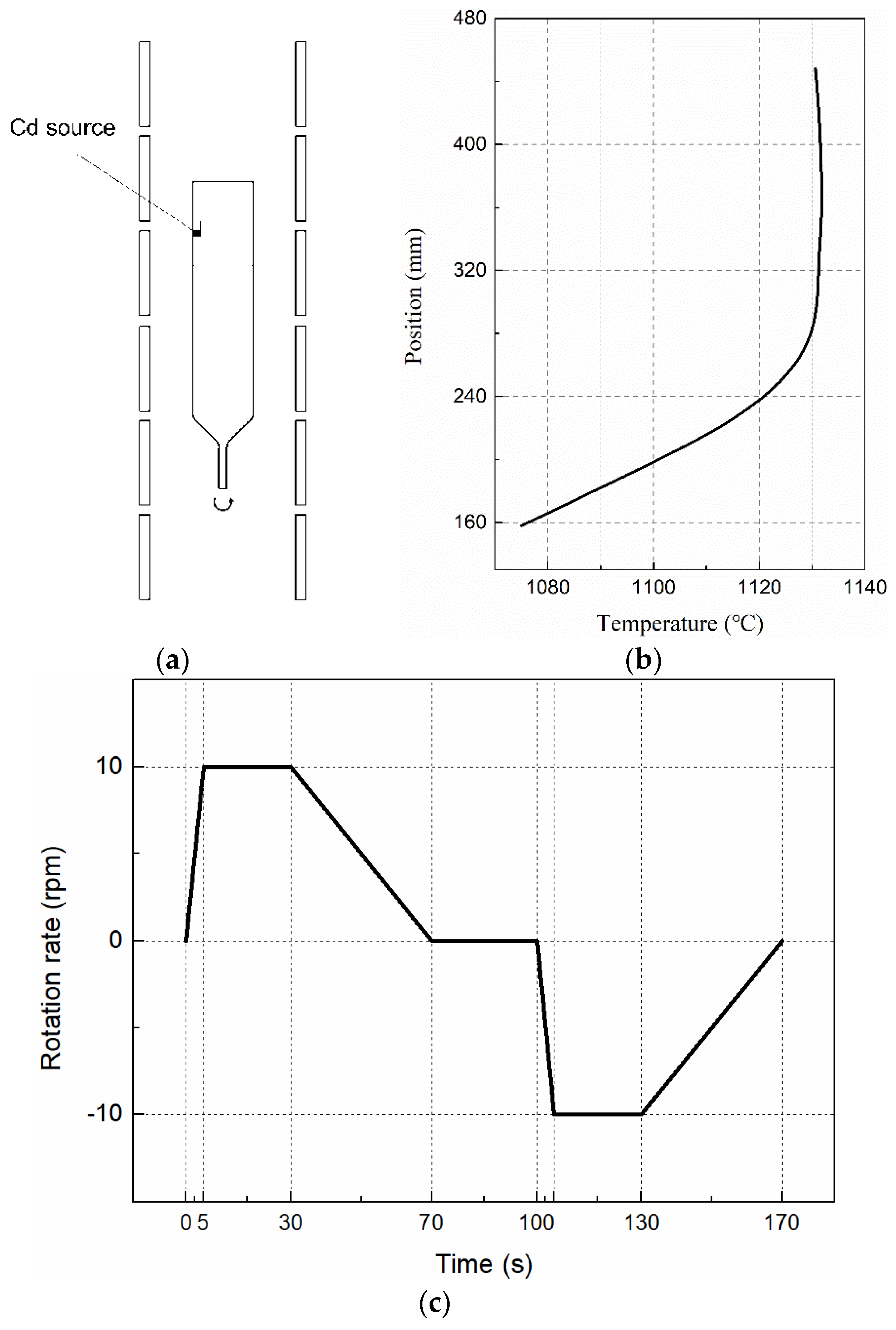
2.2. Crystal Growth and In-Situ Annealing

The additional Cd source was located away from the melt in an open capsule, as shown in Figure 1a. Figure 1b shows the experimental temperature field. The upper half of the temperature field, i.e., the high temperature zone, is nearly uniform at 1130 °C, while the temperature in the lower half has a nearly constant gradient. The cavity zone of the ampoule was held at a constant temperature throughout the growth process. Therefore, we can calculate the required quantity of Cd from the cavity volume V in the ampoule and the required vapor pressure while using the ideal gas law,
p V = n R T ,
where T is temperature, which was approximately 1403 K. The gas constant R is 8.314 J/(mol·K). The cadmium vapor pressure p is 1.3 atm, which is approximately the partial pressure of Cd0.9Zn0.1Te at this temperature, according to the P-T phase diagram [13]. n is the number of moles of Cd. Figure 1c shows the ACRT rotation sequence that was used during growth, where we used fast accelerating and slow decelerating steps. This method is effective in preventing Te accumulation at the growth interface, both at the center and near the ampoule’s inner wall [14].
Growth proceeded for approximately 10 days with 1 mm/h pulling rate followed by annealing at 850 °C for 72 h. At this temperature, Te has maximum solid solubility in CZT [13]. Therefore, annealing at this temperature causes the formation of more Te anti-sites, which ensures that the bulk resistivity is high [15]. The furnace was powered off once the annealing was completed.

2.3. Crystal Growth Results

Figure 2a shows three as-grown CZT ingots, named CZT1, CZT2, and CZT3 (from left to right, respectively). CZT1 and CZT3 have the smallest and largest grain size, respectively, which results from the continuous promotion on growth parameters. Among them, CZT3 used the optimized temperature field that is shown in Figure 1b and the ACRT sequence in Figure 1c. Figure 2b shows a wafer cut from CZT3. The uniform brightness and color of CZT3 indicate that the ingots are single-crystalline, because different crystal orientations have different optical properties. The wafers were then etched in Everson solution (HNO3:HF:lactic acid = 1:4:20). Figure 2c shows the etched wafers. Several regions with different degrees of blackening are present on the wafer cut from CZT1. However, the etched wafer cut from CZT3 has uniform color without any blackening, which shows strong evidence that the wafer is totally single-crystalline. Two-inch Cd0.9Zn0.1Te single-crystal ingots without sub-grains or twins like CZT3 were grown after several runs with optimized growth parameters, including ACRT parameters and temperature fields, as shown in Figure 2.

3. Characterization of as-Grown Ingots and Discussion

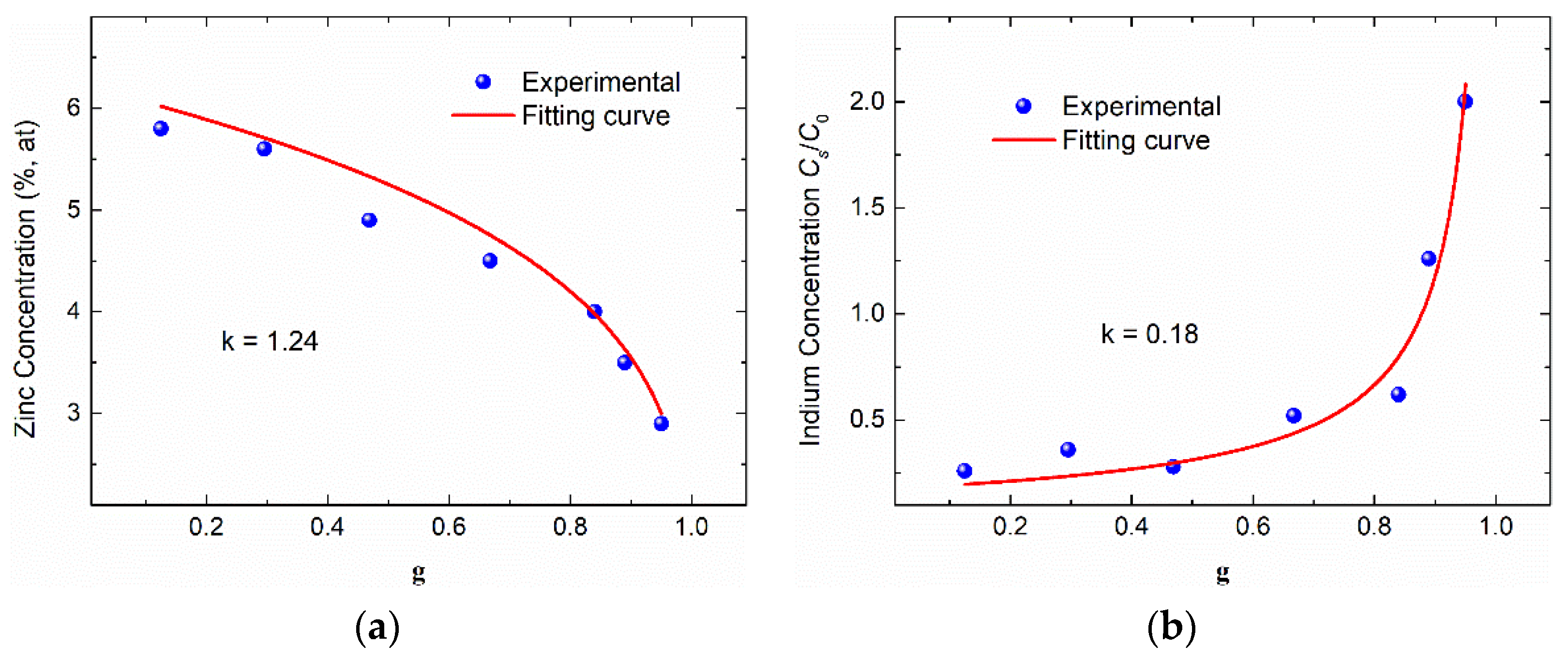
3.1. Concentration Segregation

The composition distribution of Zn and In is often used to evaluate the uniformity of the crystal. However, grain boundaries act as a region for impurity gathering [16], which will change the concentration distribution. The single crystal ingot provides more credible data for evaluating segregation during VB growth. Several 2.3 × 2.3 × 20 mm3 samples were cut from different positions along the growth direction of CZT3. Glow discharge mass spectrometry (GDMS) was used to determine the elemental concentration of Zn and In. Figure 3 shows the results, in which the following Scheil’s equation was used to fit the effective segregation coefficient [17]:
C s = C 0 k ( 1 g ) ( 1 k ) ,
where Cs is the elemental concentration at position g, C0 is the nominal concentration in the synthesized polycrystalline ingot, C0 = 5 at% for Zn, and k is the segregation coefficient. The Zn distribution that is shown in Figure 3a ranges from approximately 3 to 6 at%. The fitting curve shows that k = 1.24, which is very close to the reported value of 1.35 [18]. This indicates the melt concentration is nearly uniform during growth, because Equation (2) is based on the fully-mixed melt hypothesis. The normalized In concentration Cs/C0 in Figure 3b ranges from 0.28 to 2 with k = 0.18, whereas others reported k values that ranged from 0.04 to 0.2 [19,20,21].

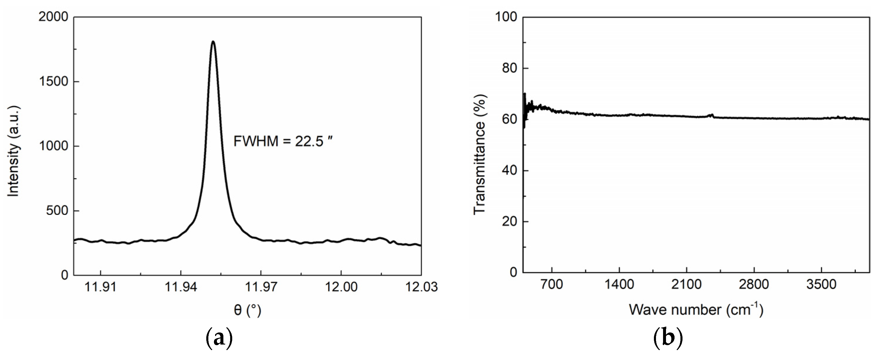
3.2. Crystallinity and Second Phase Characterizations

The crystallinity of CZT3 was investigated while using X-ray rocking curves and infrared transmittance measurements, which are shown in Figure 4. The X-ray rocking curve was measured using a Cu Kα1 X-ray source. Figure 4a shows a typical X-ray rocking curve that was gathered from CZT3, where the full width half maximum (FWHM) of the peak is approximately 22.5 ″. Figure 2c shows the radial zinc concentration in the wafer, which was indirectly measured to be approximately 4.5% to 5.0%. This range was estimated using the diffraction angles in the X-ray rocking curves and the relationship between the Zn concentration and lattice constant. The transmittance from 1000 to 4000 cm−1 wave number is approximately 61%, as shown in Figure 4b.
Te inclusion density and sizes were analyzed using IR transmission microscopy to determine the effectiveness of vapor pressure control using a Cd source during growth, and the results were compared with those from a sample without Cd source, named CZT4. IR transmission images were captured from several wafers cut from ingots CZT3 and CZT4, as shown in Figure 5. Inclusions appear to be uniformly distributed in both CZT4 and CZT3, but the inclusion sizes in CZT3 are obviously smaller than those in CZT4. Figure 5b,d show statistical data of inclusion counts and diameters. The average diameter of the inclusions in CZT4 is 23.4 μm with maximum size of approximately 40 μm, which were reduced to 13.4 μm and approximately 20 μm in CZT3, respectively. These results illustrate the effectiveness of using pressure control for controlling Te inclusions because Cd evaporation from the melt was balanced during growth, and the melt stoichiometry was maintained. The dislocations in CZT3 were also characterized by counting the etch pit density (EPD) on (111) oriented samples. The values of EPD were found to range from 1 × 10⁴ to 3 × 104 cm−2, which indicated that the sample is highly crystalline.

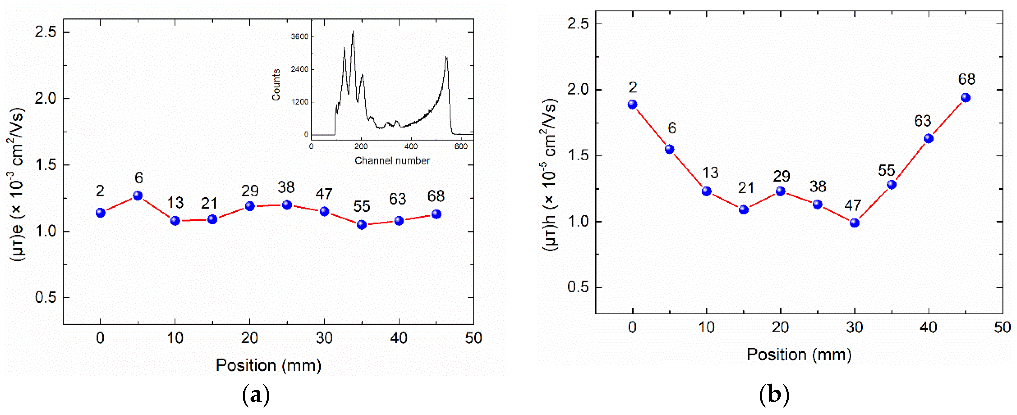
3.3. Radiation Response

The wafer in Figure 2b was fabricated into 69 parallel plane detectors (5 × 5 × 2 mm3), as shown in Figure 6a. Before measuring the radiation response, the resistivity of each detector was measured. All of the detectors had resistivity greater than 1 × 10¹⁰ Ω·cm. The radiation responses from the detectors were tested using 241[email protected] keV near the cathode. The bias voltage was set to 300 V and the shaping time was set to 5 μs. Figure 6b shows the energy resolution of all detectors, which ranges from 5.9% to 7.2%, indicating the electrical properties of the wafer are uniform. However, the peak-to-valley ratio decreased from approximately 9.5 at the wafer edge to approximately 5.9 at the center, as shown in Figure 6c.
A line of detectors from the same column in Figure 6a were selected to study the distribution of electron and hole mobility-lifetime products (μτ) values. These data were fit to the Hecht equation, which relates the bias voltages to the charge collection efficiency of the detector’s resolution response. The radiation source was located near the cathode for measuring (μτ)e for electrons, and the source was placed near the anode for hole measurements (μτ)h. These results in Figure 7a show (μτ)e ranges from 1.05 to 1.27 × 10⁻³ cm2/(V·s), and Figure 7b shows (μτ)h ranges from 0.99 to 1.94 × 10⁻⁵ cm2/(V·s). It is seen that the (μτ)e values are quite high with small deviation, but the (μτ)h values are higher near the wafer edge and lower at the wafer center. Lower (μτ)h values at the wafer center mean significant peak tailing, which decrease the peak-to-valley ratios [22]. We consider non-uniform (μτ)h values to be the reason for the non-uniform peak-to-valley ratios that are shown in Figure 6c. One of the possible explanations might be the different concentrations of Cd vacancies and Te interstitials, which are lower near the edge of the ingot and higher in the center. These defects are acceptors and they are known to act as hole traps [23,24].

4. Conclusions

In this work, we successfully grew single-crystal Cd0.9Zn0.1Te ingots while using the VB method with ACRT and Cd source for vapor pressure control. The entire ingot was free of grain boundaries and twins. The segregation coefficients of Zn and In were determined to be 1.24 and 0.18, respectively. The average diameter of Te inclusions was 13.4 μm with a maximum value of approximately 20 μm. The FWHM of an X-ray rocking curve was approximately 22.5 ″, IR transmittance was approximately 61%, and the EPD value is less than 3× 104 cm−2. The detectors’ response to 59.5 keV gamma ray from 241Am shows a uniform response with energy resolution that ranged from 5.9% to 7.6%. The peak-to-valley ratio decreases from 9.5 at the wafer edge to 5.9 at the center. The (μτ)e values were found to range from 1.05 to 1.27 × 10⁻³ cm2/V·s, and (μτ)h ranged from 0.99 to 1.94 × 10⁻³ cm2/V·s.

Author Contributions

F.Y. proposed the growth method, analyzed and investigated the experimental results, and wrote the manuscript. W.J. supported resources, funded the research and revised the manuscript. M.W. processed part of the experimental data and did some growth simulations. X.S. optimized the growth methods and prepared for growth. N.J. processed and analyzed part of the experimental data. L.Y. modeling and simulations of growth. B.Z. helped analyzing the results. T.W. funded and led the project, optimized the growth method and revised the manuscript. All authors have read and agreed to the published version of the manuscript.

Funding

This work was funded by the National Natural Science Foundation of China (Grant No.51672216, Grant No.51702271), the National Key R&D Program of China (Grant No.2016YFB0402405, 2016YFF0101301), the Fundamental Research Funds for the Central Universities (Grant No.3102019ghxm015) and the Research Fund of the State Key Laboratory of Solidification Processing (NPU), China (Grant No.2019-TS-05).

Conflicts of Interest

The authors declare no conflict of interest.

References

  1. Eisen, Y.; Shor, A.; Mardor, I. CdTe and CdZnTe gamma ray detectors for medical and industrial imaging systems. J. Cryst. Growth 1999, 428, 158–170. [Google Scholar] [CrossRef]
  2. Carini, G.A.; Arnone, C.; Bolotnikov, A.E.; Camarda, G.S.; De Wames, R.; Dinan, J.H.; Markunas, J.K.; Raphothamachar, B.; Sivananthan, S.; Smith, R.; et al. Material quality characterization of CdZnTe Substrates for HgCdTe epitaxy. J. Electron. Mater. 2006, 35, 1495–1502. [Google Scholar] [CrossRef] [Green Version]
  3. Schwenkenbecher, K.; Rudolph, P. Investigation of convection in the solution zone at the growth of CdTe by THM. Cryst. Res. Technol. 1985, 20, 1609–1613. [Google Scholar] [CrossRef]
  4. Rudolph, P.; Muhlberg, M. Basic problems of vertical Bridgman growth of CdTe. Mater. Sci. Eng. B 1993, 16, 8–16. [Google Scholar] [CrossRef]
  5. Shcherbak, L.; Feychuk, P.; Plevachuk, Y.; Dong, C.; Kopach, O.; Panchuk, O.; Siffert, P. Structure rearrangement of the Cd1-xZnxTe (0 < x < 0.1) melts. J. Alloys Compd. 2004, 371, 186–190. [Google Scholar]
  6. Chen, H.; Awadalla, S.A.; Iniewski, K.; Lu, P.H.; Harris, F.; Mackenzie, J.; Hasanen, T.; Chen, W.; Redden, R.; Bindley, G. Characterization of large cadmium zinc telluride crystals grown by travelling heater method. J. Appl. Phys. 2008, 103, 014903. [Google Scholar] [CrossRef] [Green Version]
  7. Zappettini, A.; Zambelli, N.; Benassi, G.; Calestani, D.; Pavesi, M. Live-monitoring of Te inclusion laser-induced thermo-diffusion and annealing in CdZnTe crystal. Appl. Phys. Lett. 2014, 104, 252105. [Google Scholar] [CrossRef]
  8. Szeles, C.; Cameron, S.E.; Soldner, S.A.; Ndap, J.; Reed, M.D. Development of the high-pressure electro-dynamic gradient crystal-growth technology for semi-insulationg CdZnTe growth for radiation detector applications. J. Electron. Mater. 2004, 33, 742–751. [Google Scholar] [CrossRef]
  9. Franc, J.; Sedivy, L.; Belas, E.; Bugar, M.; Zazvorka, J.; Pekarek, J.; Uxa, S.; Hoschl, P.; Fesh, R. Mealt growth and post-grown annealing of semiinsulating (CdZn)Te by vertical gradient freeze method. Cryst. Res. Technol. 2013, 48, 214–220. [Google Scholar] [CrossRef]
  10. Azoulay, M.; Zilber, R.; Shusterman, S.; Goldgirsh, A.; Zontag, I. Growth and characterization of CdTe and CdZnTe crystals for substrate application. Proc. SPIE 2003, 4820, 790–808. [Google Scholar]
  11. Wang, T.; Ai, X.; Yin, Z.; Zhao, Q.; Zhou, B.; Yang, F.; Xu, L.; Zha, G.; Jie, W. Study on a co-doped CdZnTe crystal containing Yb and In. Cryst. Eng. Comm. 2019, 21, 2620–2625. [Google Scholar] [CrossRef]
  12. Rudolph, P.; Koh, H.J.; Schafer, N.; Fukuda, T. The crystal perfection depends on the superheating of the mother phase too-experimental facts and speculations on the “melt structure” of semiconductor compounds. J. Cryst. Growth 1996, 166, 578–582. [Google Scholar] [CrossRef]
  13. Greenberg, J.H. P-T-X phase equilibrium and vapor pressure scanning of non-stoichiometry in the Cd-Zn-Te system. Prog. Cryst. Growth Charact. Mater. 2003, 47, 196–238. [Google Scholar] [CrossRef]
  14. Yin, L.; Jie, W.; Wang, T.; Zhou, B.; Yang, F.; Nan, R. The effects of ACRT on the growth of ZnTe crystal by the temperature gradient solution growth technique. Crystals 2017, 7, 82. [Google Scholar] [CrossRef] [Green Version]
  15. Babentsov, V.; Franc, J.; Hoeschl, P.; Fiederle, M.; Benz, K.; Sochinskii, N.; Dieguez, E.; James, R. Characterization of compensation and trapping in CdTe and CdZnTe: Recent advances. Cryst. Res. Technol. 2009, 44, 1054–1058. [Google Scholar] [CrossRef]
  16. Heffelfinger, J.R.; Medlin, D.L.; James, R.B. Structural and chemical analysis of grain boundaries and tellurium precipitates in commercial Cd1-xZnxTe. Proc. SPIE 1998, 3446, 49–54. [Google Scholar]
  17. Sheil, E. Bemerkungen zur schichtkristallbildung. Z. Metallkd 1942, 34, 70–72. [Google Scholar]
  18. Tanaka, A.; Masa, Y.; Seto, S.; Kawasaki, T. Zinc and selenium co-doped CdTe substrates lattice matched to HgCdTe. J. Cryst. Growth 1989, 94, 166–170. [Google Scholar] [CrossRef]
  19. Yokota, K.; Nakai, H.; Satoh, K.; Katayama, S. Segregation coefficients and activation of indium in cadmium telluride grown from tellurium-rich melt by the Bridgman technique. J. Cryst. Growth 1991, 112, 723–728. [Google Scholar] [CrossRef]
  20. Weigel, E.; Muller-Vogt, G.; Steinbach, B.; Wendl, W.; Stadler, W.; Hofmann, D.M.; Meyer, B.K. Defects and electrical properties of doped and undoped CdTe single crystals from tellurium-rich solutions. Mater. Sci. Eng. B 1993, 16, 17–22. [Google Scholar] [CrossRef]
  21. Fochuk, P.; Panchuk, O.; Feychuk, O.; Shcherbak, L.; Savitskyi, A.; Parfenyuk, O.; Ilashchuk, M.; Hage-Ali, M.; Siffert, P. Indium dopant behavior in CdTe single crystals. Nucl. Instr. Meth. Phys. Res. Sect. A 2001, 458, 104–112. [Google Scholar] [CrossRef]
  22. Parnham, K.; Szeles, C.; Prettyman, T.H.; Smith, M.; Stahle, C.; Parker, B.H.; Wang, L.L. Further studies on the modified two-terminal electrode geometry for CdZnTe detectors. Nucl. Instr. Meth. Phys. Res. Sect. A 2001, 458, 334–338. [Google Scholar] [CrossRef]
  23. Huang, Z.C.; Eissler, E.; Wie, C.R. Role of cadmium vacancy-related defects in CdTe nuclear detectors. Nucl. Instr. Meth. Phys. Res. Sect. A 1995, 100, 507–510. [Google Scholar] [CrossRef]
  24. Carvalho, A.; Oberg, S.; Briddon, P.R. Intrinsic defect complexes in CdTe and ZnTe. Thin Solid Films 2011, 519, 7468–7471. [Google Scholar] [CrossRef]
Figure 1. (a) Ampoule with an additional Cd source, (b) axial distribution of the temperature field, and (c) accelerated crucible rotation technique (ACRT) sequence used during the growth process.
Crystals 10 00261 g001
Figure 2. (a)As-grown Cd1-xZnxTe (CZT) ingots, (b) single-crystalline wafer cut from ingot CZT3, and (c) wafer etched with the Everson solution; the major shows the wafer cut from CZT3, and the inset shows the wafer cut from CZT1.
Crystals 10 00261 g002
Figure 3. Elemental concentration along the growth direction measured using GDMS. (a) Zn distribution and (b) normalized In distribution. g is the normalized axial position in the ingot, where g = 0 corresponds to the tip of the ingot, and g = 1 is the tail of the ingot. The solid blue circles show experimental results and the red solid lines are fitting curves modeled using Equation (2).
Crystals 10 00261 g003
Figure 4. Crystallinity of CZT3: (a) X-ray rocking curve and (b) IR transmittance.
Crystals 10 00261 g004
Figure 5. (a) and (c) IRTM images of Te inclusions in CZT4 and CZT3, respectively; (b) and (d) statistical data showing inclusion numbers and diameters in CZT4 and CZT3, respectively.
Crystals 10 00261 g005aCrystals 10 00261 g005b
Figure 6. Detector properties under irradiation of 241[email protected] keV; (a) numbered detectors on a wafer, (b) energy resolution, and (c) peak-to-valley ratio.
Crystals 10 00261 g006
Figure 7. Mobility-lifetime products of detectors from the same column: (a) (μτ)e and (b) (μτ)h values. The inset in (a) shows a typical radiation response spectrum for detector No. 68. The numbers above the data points in the figures show the corresponding detector number in Figure 6a.
Crystals 10 00261 g007

