Abstract
The research on anti-reflection (AR) optical thin film has long sought to obtain high-performance reflection and transmission properties in photovoltaic and photonic devices. The study of multi-layer AR (M-AR) film with low- and high-refractive-index materials is essential to increase the selective transmittance and reflectance at visible light wavelengths. However, M-AR film exhibits low substrate adhesion and slow deposition rates. We developed a DC pulse sputter system incorporating an inductively coupled plasma (ICP) source of high density to obtain high-quality M-AR film. Six-layer AR optical thin film was simulated using SiOx as a low-refractive-index material and NbOx as a high-refractive-index material. The multi-layer AR film based on SiOx and NbOx (M-SiNb) was fabricated using DC pulse sputtering which incorporated an ICP source. M-SiNb film exhibited better properties than the optical simulation results at 550 nm (transmittance: 99.19%, reflectance: 0.87%). Similarly, the M-SiNb film fabricated using the ICP source had high transmittance and reflectance in the visible light region and excellent adhesion to the substrate notwithstanding the various mechanical tests it was subjected to. Consequently, the development of the DC pulse sputter system included the ICP source, and this study represents important research in the field of optical film.
1. Introduction
The transmittance and reflectance of optical thin film can be adjusted in a specific wavelength range according to its purpose [1,2,3]. In particular, an anti-reflection (AR) film reduces the reflection intensity and increases the quality of optical characteristics; hence, it plays an important role in the manufacturing of optical instruments such as lenses, solar cells, and flat panel displays [4]. The principle of AR film lies in the destructive interference of reflected light from the interface of the air and the film substrate. The amplitude of reflected light from the substrate surface should be matched by the amplitude of reflected light from the AR film surface. The choice of AR film material is an important factor in the destructive interference of reflected light. Common AR film consists of multi-layered film with alternating high- and low-refractive-index materials, typically making use of transparent materials such as SiO2, Nb2O5, TiO2, MgF2, and indium-tin oxide (ITO) [5,6]. Among these AR film materials, the visible light range has been studied most due to the specific properties exhibited here. SiOx is a refractive material, with excellent optical properties (refractive index: 1.46) among low-refractive-index materials. It is also inexpensive compared to other low-refractive-index materials. NbOx also has excellent optical properties (refractive index: 1.53) and a smaller absorption coefficient than other high-refractive-index materials [7,8,9,10,11].
Reactive radio frequency (RF) sputtering technology [12,13], one of the most accurate methods of depositing oxide thin films, can produce high-quality thin films from high melting-point materials. Moreover, the deposited AR film can easily attain the same chemical composition as that of its target. However, since the reactive RF sputtering technique has the disadvantages of having a slow deposition rate, poor step coverage, surface roughness, and poor substrate durability, it remains problematic for the production of high-quality optical thin film [14,15]. To solve this, plasma source antennas have been used for the deposition of high-quality AR film. One of the plasma sources, an inductively coupled plasma (ICP) source antenna, is coil-shaped, and when RF power is applied to the antenna, a current flows in it creating an induction field around the antenna. Because of these properties, the use of existing plasma sources has been reduced and interest in ICP plasma source methods has soared in the field of AR film deposition. The induction field is a factor that creates the high-density ICP source and maintains it. Furthermore, the AR film boasts a fast deposition rate and a uniform surface according to the increase in temperature of the electron beam [16,17,18,19,20,21]. Therefore, binary materials such as oxides (SiOx and NbOx) have poor hardness and wear resistance but this method reduces these properties. Additionally, it reduces defects such as scratches, residues, and peeling in various external environments, and can rapidly deposit high-density layers of AR film. Although it may be difficult to expect good interfacial adhesion due to the large lattice constant differences between the low- and high-refractive-index materials, the adhesion between the interfaces can be improved using the high-density ICP source.
In this study, we designed and manufactured a DC pulse sputter system with an ICP radical source. We fabricated a single-layer AR film using this DC pulse sputter system (with the ICP source) and observed a fast deposition rate and a uniformity of AR thin film with the ICP source, which exhibited better properties than without the ICP source. The multilayer AR film was designed using the properties of single-layer AR film [22]. SiOx and NbOx were used as the low- and high-refractive-index materials of the AR film, respectively. We measured the optical properties of SiOx and NbOx two-single-layer AR films at the visible region using UV-visible spectroscopy (UV-vis) and designed the multilayer AR film using these properties. Finally, we fabricated the high-quality multilayer AR film based on SiOx and NbOx (M-SiNb) using the DC pulse sputter system (with the ICP source). We compared the uniformity of the surface of the two single-layer AR films with the ICP source with AR films fabricated without the ICP source. The hardness of the SiOx and NbOx was 1.1 and 1.5 times stronger, respectively, than without the ICP source. The M-SiNb with the ICP source also had better uniformity of surface compared to AR films fabricated without the ICP source. The M-SiNb fabricated with the ICP source maintained the durability and stability of the AR film without a change of refractive index after the constant temperature and humidity and saline spray tests. The results show that the fabricated sputter system and AR film can be used in optical lenses, camera lenses, smartphone displays, and solar cell applications.
2. Materials and Methods
2.1. Materials
Si and Nb targets (430 × 100 × 10 T/purity: 9.99 %) were purchased from Taewon Scientific Co., Ltd. (Seoul, South Korea) and O2 gas was purchased from Seonggwang Oxygen Co. (Gimhae, South Korea). They were used as deposition materials for the fabrication of M-SiNb film. Slide glass (Schott B270/50×25×1 T) was purchased from P&Tech (Cheongju, South Korea) and used as the substrate for the AR film. The Macleod software package (11.0.537, Thin Film Center Inc., Tucson, AZ, USA) is a program for optical thin film design and was used for the design of the M-SiNb film. The ICP source was purchased from UNIVAC (Gimhae, Korea) and was used for manufacturing the DC pulse sputter system with the ICP source.
2.2. Characteristics
UV-vis (Lambda 950, PerkimElmer, USA) was used to measure the transmittance and reflectance of the AR films, and the transmittance and reflectance indexes were used when the M-SiNb film was designed. The morphologies of both the SiOx and NbOx single-layer AR films and the M-SiNb film were investigated using field-emission secondary electron microscopy (FE-SEM; S-4300, Hitachi, Tokyo, Japan), and atomic force microscopy (AFM; XE-100, Park systems, Suwon, South Korea). The hardness of the SiOx and NbOx single layers were measured using a hardness tester (Nano indentation tester: NHT3, Anton Paar, Austria). A constant temperature and humidity tester (TH-ME-025, Jeio tech, Busan, Korea) and a saltwater spray tester (VT-ST 100, visiontec21, Daegu, Korea) were used for durability and stability tests of the M-SiNb film.
2.3. Fabrication of High-Quality Multi-Layers AR Film Based on SiOx and NbOx (M-SiNb)
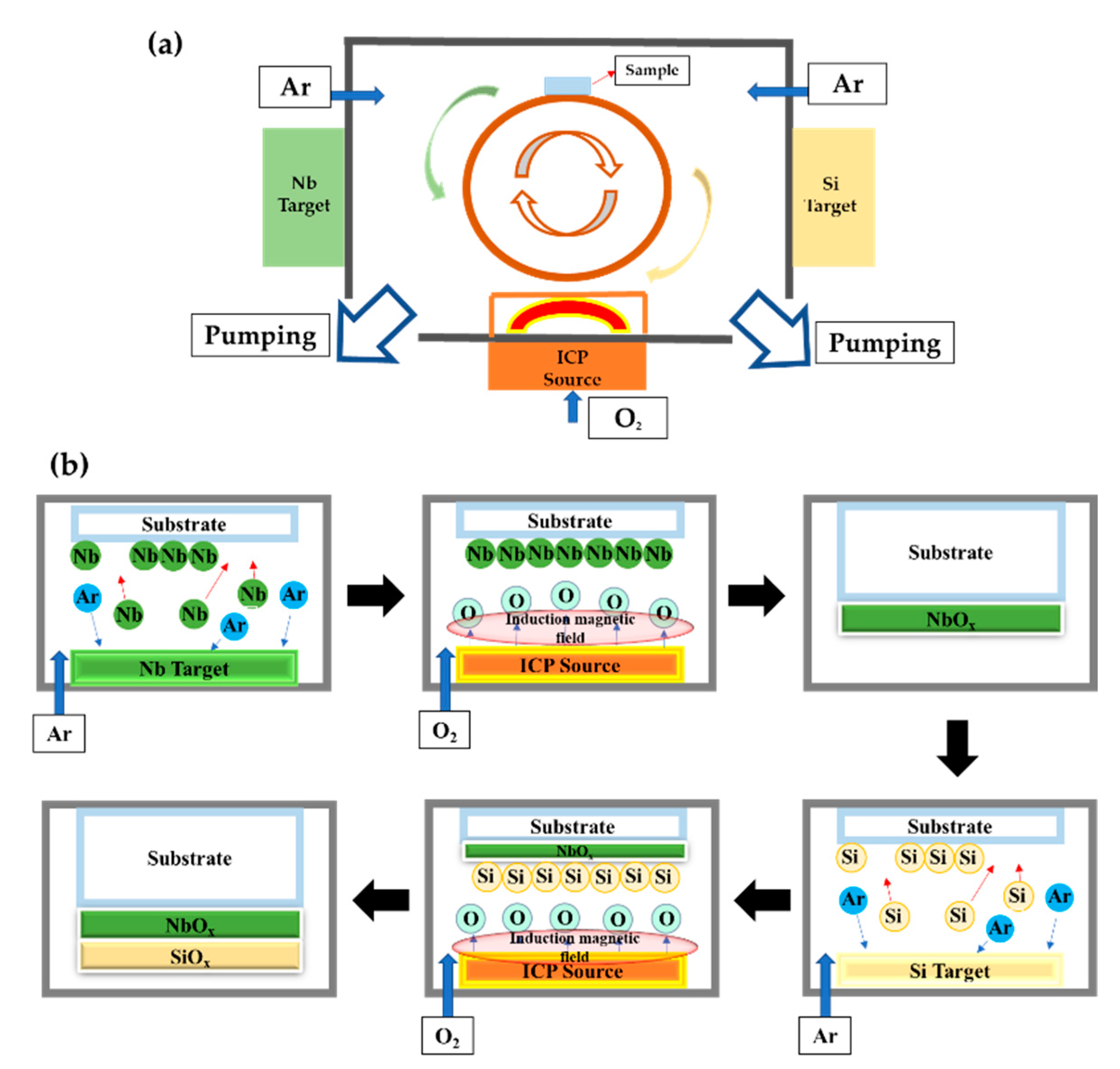
Figure 1a shows a schematic diagram of the DC pulse sputter system with the ICP source. For mass production of the AR film, we used a drum-type sample holder. The Si target was mounted on the right side of the chamber, the Nb target on the left side, and the ICP source was mounted on the door of the chamber. The O2 gas flowed at the point at which the ICP source was installed. A shutter was installed at each target to prevent the mixing of each of the target materials. The pumping system between the target and the ICP source played a target oxidation prevention role. The deposition process of the M-SiNb film using our manufactured DC pulse sputter system with the ICP source is shown in Figure 1b. The distance of target and substrate was 110 mm, and process temperature and power were 60 ℃ and 3000 W, respectively. The sample holder was turned clockwise when the SiOx film was deposited and turned counterclockwise when the NbOx film was deposited. First, when the NbOx film was deposited, the deposition pressure was 3 mTorr, and the flow rate of O2 and Ar gases was 200 and 100 sccm, respectively. And, when the SiOx film was deposited, the deposition pressure was 1 mTorr, and the flow rate of O2 and Ar gases was 150 and 100 sccm, respectively. Finally, the two AR films were deposited alternately, layer by layer, to fabricate the M-SiNb film.

Figure 1.
Schematic diagram of (a) the manufactured DC pulse sputter system with the inductively coupled plasma (ICP) source and (b) process of deposited M-SiNb using the ICP source.
3. Results
3.1. Characteristics of SiOx and NbOx Single Layer
We first measured the cross-sections of the SiOx and NbOx samples using FE-SEM to design the AR multilayer films based on SiOx and NbOx. Figure 2 shows the cross-sectional and top views of the SiOx and NbOx single-layer AR films with and without the ICP source. As seen in Figure 2a–d, the surface differences of SiOx are hard to observe. However, for the surface of NbOx using the ICP source, it was observed that it has a smoother surface than the surface of NbOx not using ICP source.
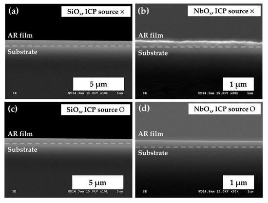
Figure 2.
Cross-sectional SEM mages SiOx and NbOx single-layer anti-reflection (AR) films; (c,d) without and (a,b) with the ICP source.
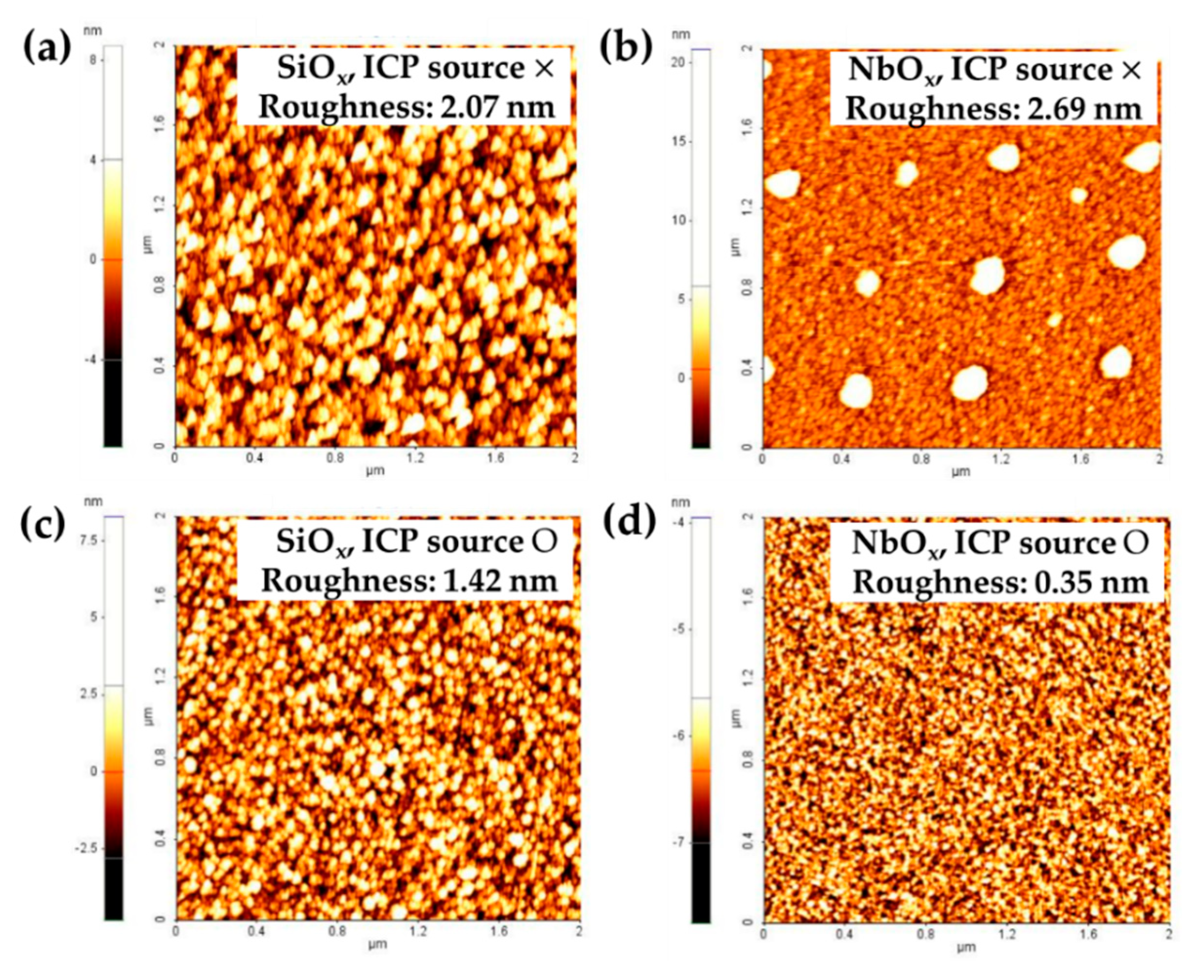
Moreover, the Figure 3a–d shows the surface roughness of AR coating films to observe clear differences of sample surfaces. The surface roughness of samples (SiOx: 1.42 nm, NbOx: 0.35 nm) using an ICP source is lower than the surface roughness of samples (SiOx: 2.07 nm, NbOx: 2.69 nm) not using an ICP source. Therefore, the AR films using the high-density radical source had a more uniform layer and smoother surface than the films not using it.

Figure 3.
AFM images of deposited SiOx and NbOx single-layer anti-reflection (AR) films; (c,d) without and (a,b) with the ICP source.
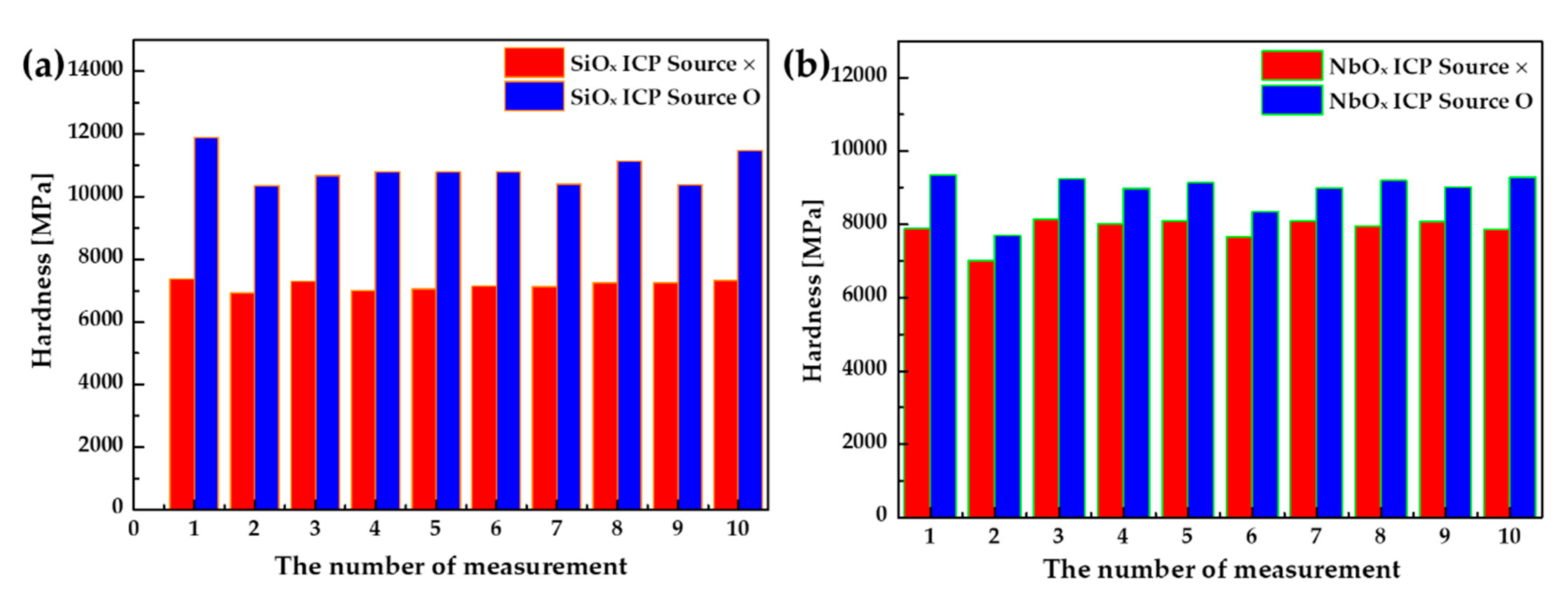
Figure 4 shows the single-layer hardness results of the SiOx and NbOx samples. The hardness of the deposited single-layer AR films using the ICP source was stronger than the deposited single-layer AR films not using it. The hardness difference of the SiOx and NbOx films using the ICP source was 1.5 times and 1.1 times higher, respectively, than not using the ICP source. Consequently, the deposited multilayer AR films using the ICP source were expected to have better durability than those not using the ICP source.
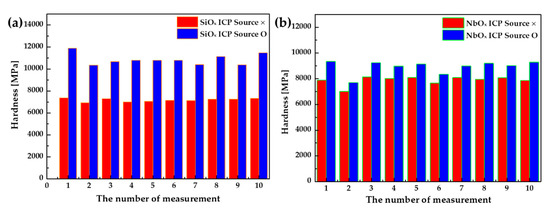
Figure 4.
Hardness of single-layer AR films according to the presence or absence of the ICP source; (a) SiOx and (b) NbOx.
In addition, we measured the transmission and reflectance of the SiOx and NbOx single-layer AR films using ultraviolet-visible spectrophotometry (UV-vis). The transmission and reflectance of SiOx and NbOx were used for the design of a multilayer AR film based on SiOx and NbOx (M-SiNb) using the Macleod software. The simulated M-SiNb film consisted of a total of six layers with alternating SiOx and NbOx on a glass substrate as shown in Figure 4a,b. Figure 4c,d show the transmission and reflectance of the designed M-SiNb film according to the presence or absence of the ICP source in the visible region using the Macleod simulation software. The reflectance and transmittance of the M-SiNb film using the ICP source was 0.2% lower and 0.28% higher, respectively, than without the ICP source at 550 nm. The results suggest that our manufactured DC pulse sputter system (incorporating the ICP source) produced excellent AR coatings for optical thin films.
3.2. Characteristics of the Multi-Layer AR Film Based on SiOx and NbOx (M-SiNb)
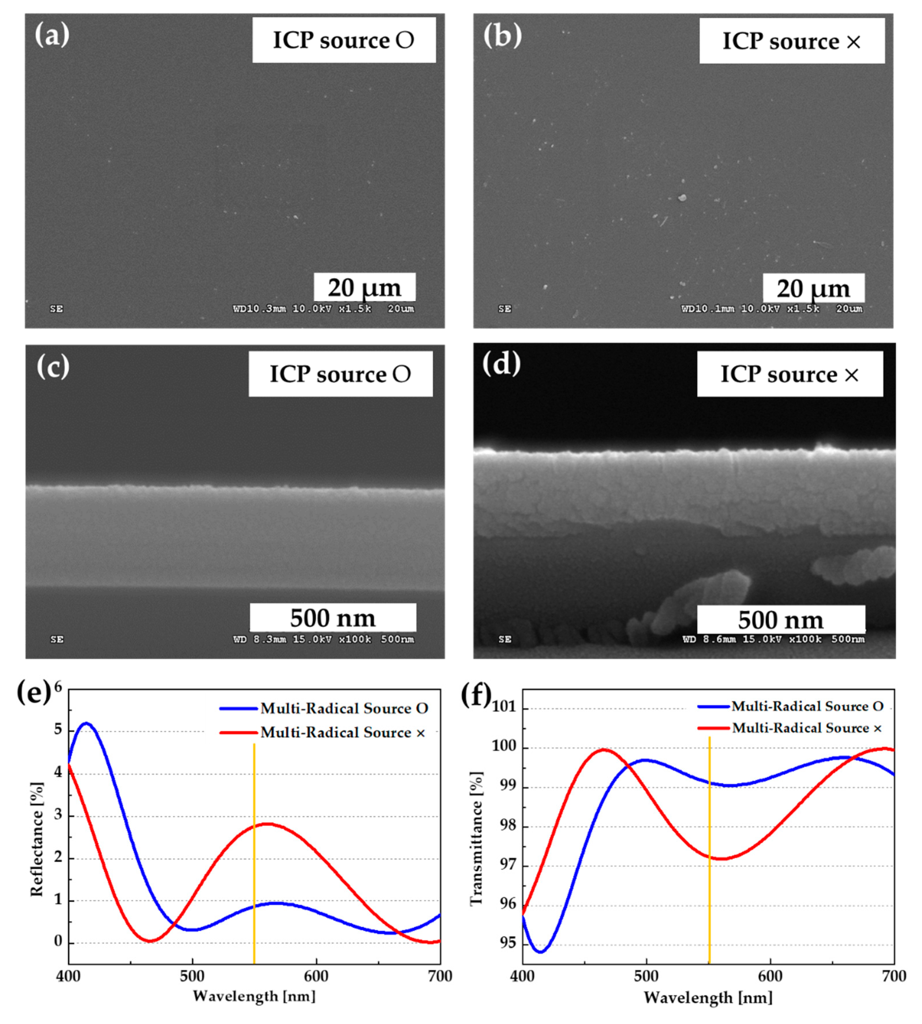
The designed six-layer M-SiNb film was subjected to a deposition experiment which differed depending on the presence or absence of the ICP source. Top views and cross-sections of the M-SiNb film were measured using FE-SEM to observe the morphology of the M-SiNb film. Figure 5a–d shows the top-view and cross-sectional images of the M-SiNb film according to the presence or absence of the ICP source. The deposited M-SiNb film using the ICP source had a more uniform surface and cross-section than the film not using the ICP source. We measured the transmittance and reflectance of the deposited M-SiNb film by DC pulse sputtering as shown in Figure 6e,f. The reflectance and transmittance of the M-SiNb film using the ICP source was about 0.87% and 99.19% at 550 nm, respectively. These values were about 1.89% lower (reflectance) and 1.95% higher (transmittance), respectively, compared with the deposited M-SiNb film not using the ICP source. Moreover, the reflectance and transmittance of the deposited M-SiNb film using the ICP source had 3.35% lower and 3.41% higher values compared with the simulated M-SiNb film (reflectance: 4.22%, transmittance: 95.78%), respectively.
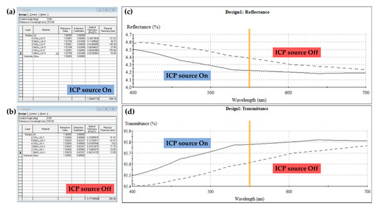
Figure 5.
The simulation results of M-SiNb (a) with and (b) without the ICP source. (c) Reflectance and (d) transmittance of the simulated M-SiNb according to the presence or absence of the ICP source.
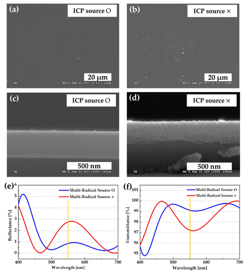
Figure 6.
Top-view and cross-sectional SEM images of deposited M-SiNb (a,c) using the ICP source and (b,d) not using the ICP source. (e) Reflectance and (f) transmittance of the deposited M-SiNb according to the presence or absence of the ICP source.
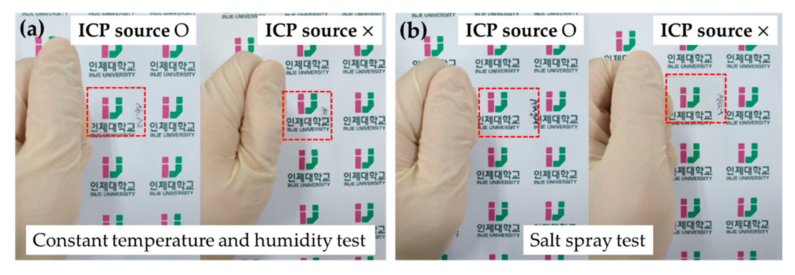
In addition, the constant temperature and humidity and salt spray tests of the M-SiNb film were performed to observe the durability of the optical thin film according to the presence or absence of the ICP source. Figure 7 shows the images of the M-SiNb film depending on the presence or absence of the ICP source after the constant temperature and humidity and salt spray tests. The M-SiNb samples were seen to be transparent regardless of the ICP source and the constant temperature and humidity and salt spray tests. Since any change of the thin film (according to the ICP source) could not be visually observed, the morphologies of samples were investigated using FE-SEM, and the refractive index was confirmed by measuring the transmittance and reflectance of the sample by means of UV-vis.
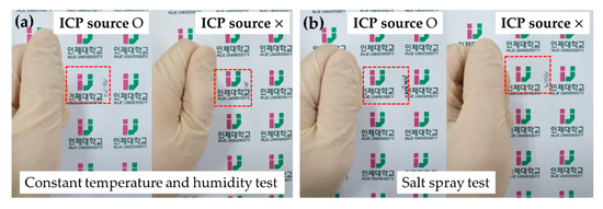
Figure 7.
Images of the M-SiNb film after testing; (a) constant temperature and humidity test and (b) saltwater test.
Figure 8 shows the SEM images of the M-SiNb film depending on the presence or absence of the ICP source after the constant temperature and humidity and salt spray tests. Top views of the M-SiNb film were measured using FE-SEM to observe the morphology and peeling phenomenon of the M-SiNb film. The deposited M-SiNb film using the ICP source had a more uniform surface than the film not using the ICP source and exhibited no peeling phenomenon. In particular, the morphologies of the sample with the ICP source maintained a smooth surface compared with the samples before constant temperature and humidity and salt spray tests of Figure 5. The results suggest that the availability of the DC pulse sputter system (incorporating the ICP source) proved to produce good multilayer AR coatings of optical thin films.

Figure 8.
The SEM images of the M-SiNb according to the presence or absence of the ICP source after testing; (a,b) constant temperature and humidity test and (c,d) saltwater test.
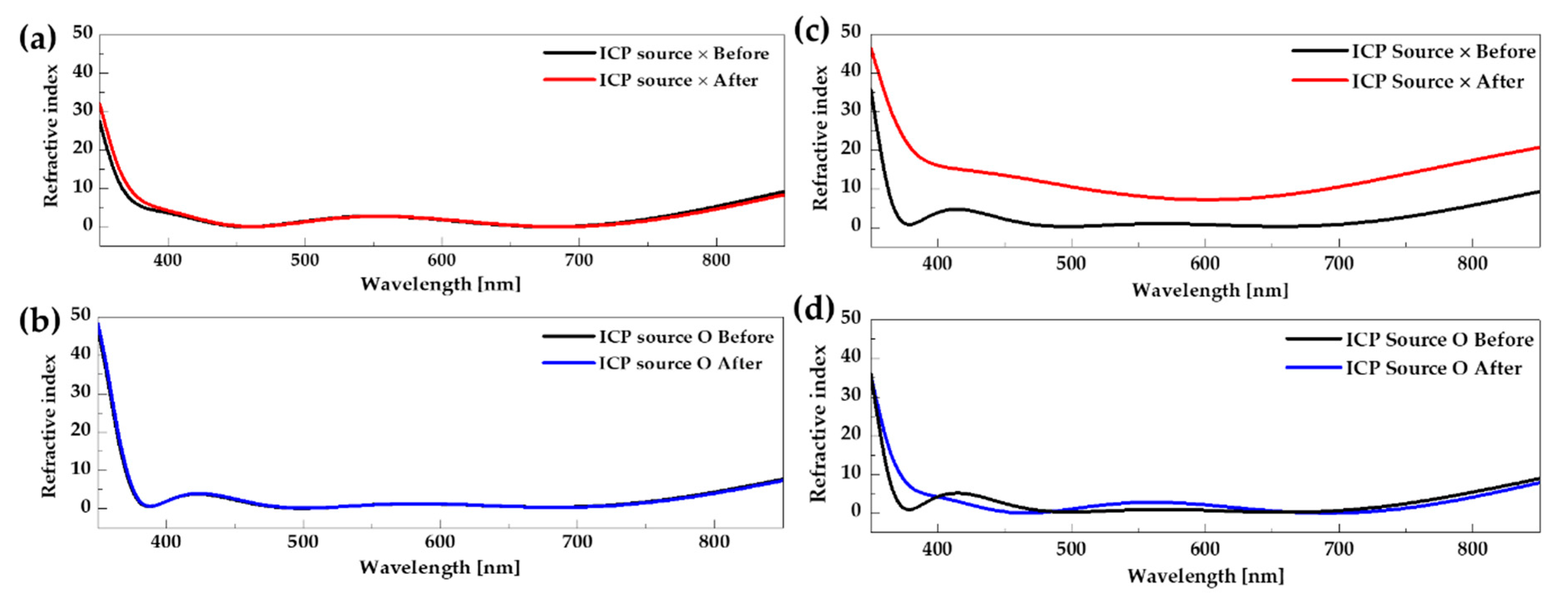
Figure 9a,b shows the refractive index before and after the constant temperature and humidity test of the M-SiNb film depending on the presence or absence of the ICP source. The refractive index of the M-SiNb film using the ICP source was compared before and after the constant temperature and humidity test, and it was confirmed that both M-SiNb films, regardless of the ICP source, had similar refractive index values. However, the refractive index of the M-SiNb films with and without the ICP source were about 1.03 and 2.75, respectively, which means that the M-SiNb film with the ICP source was deposited more uniformly than the M-SiNb film without the ICP source. The refractive index of the M-SiNb film, according to the presence or absence of the ICP sources before and after the salt spray test are shown in Figure 8c,d [23]. A comparison of the refractive index of the M-SiNb film before and after the salt spray test showed a change from 0.87 to 2.76 (ICP source O) and from 0.92 to 8.17 (ICP source ×), respectively, depending on the presence or absence of the ICP source. The M-SiNb film exhibited better durability overall in the constant temperature and humidity test than in the saltwater test. The M-SiNb film with the ICP source, exhibited good durability in both the constant temperature and humidity test and the saltwater test. Therefore, the results suggest that the ICP source created a superior AR coating of the optical thin film. The DC pulse sputter system with the ICP source was successfully developed, and the six-layer M-SiNb film did not peel from the substrate, demonstrating excellent durability in various environments.
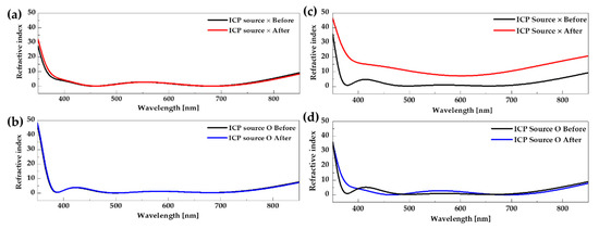
Figure 9.
The refractive index of the M-SiNb according to the presence or absence of the ICP source; (a,b) the constant temperature and humidity test and (c,d) saltwater test.
4. Conclusions
We successfully manufactured a DC pulse sputter system including an ICP source for the deposition of a six-layer AR optical film of high durability. The hardness values of the single-layer SiOx and NbOx films with the ICP source were 1.5 and 1.1 times stronger, respectively, than without the ICP source. The transmittance (95.78%) and reflectance (4.22%) values of the designed M-SiNb film using the ICP source were similar to the measured values (transmittance: 99.19%, reflectance: 0.87%) of the deposited M-SiNb film at 550 nm. The deposited M-SiNb film using the ICP source had a uniform surface despite the fast deposition rate. It also had a 2.7 and 3.0 times higher refractive index than the M-SiNb film not using the ICP source after the constant temperature and humidity and saltwater tests, respectively. The deposited M-SiNb film using the ICP source exhibited no peeling phenomenon throughout various tests (constant temperature and humidity, saline spray, and hardness). Consequently, the fabricated DC pulse sputter system and resultant M-SiNb film will have a positive effect on various optical film applications in the fields of, among others, optical lenses, camera lenses, smartphone displays, and solar cells.
Author Contributions
Formal analysis, H.L. and B.K.; investigation, B.K.; data curation, H.L. and M.P.; writing—original draft preparation, H.L.; writing—review and editing, M.P.; supervision, M.J.; project administration, M.J.; All authors have read and agreed to the published version of the manuscript.
Funding
This research was supported by Fostering Regional Flagship Industries Program through the Korea Institute for Advancement of Technology (KIAT) funded by the Ministry of SMEs and Startups (G02P02670035502).
Acknowledgments
This research was supported by Fostering Regional Flagship Industries Program through the Korea Institute for Advancement of Technology (KIAT) funded by the Ministry of SMEs and Startups (G02P02670035502).
Conflicts of Interest
The authors declare no conflict of interest.
References
- Kim, M.; Kang, T.W.; Kim, S.H.; Jang, E.H.; Park, H.H.; Seo, J.; Lee, S.J. Antireflective, self-cleaning and protective film by continuous sputtering of a plasma polymer on inorganic multilayer for perovskite solar cells application. Sol. Energy Mater. Sol. Cells 2019, 191, 55–61. [Google Scholar] [CrossRef]
- Castellón, E.; Zayat, M.; Levy, D. Sol-gel materials for electro-optical and optically active humidity-sensitive devices. J. Solgel Sci. Technol. 2019, 89, 56–61. [Google Scholar] [CrossRef]
- Ying, S.P.; Fu, H.K.; Hsieh, H.H.; Wu, J.H. Optical film design of low-glare LED panel light. Opt. Laser Technol. 2019, 111, 45–50. [Google Scholar] [CrossRef]
- Kim, J.; Song, S.; Kim, Y. A Basic Study on Anti-reflection Coating PV Technology for Reducing Reflected Sunlight on the Building Skin. Asia-pacific Journal of Convergent Research Interchange 2019, 5, 23–30. [Google Scholar] [CrossRef]
- Macleod, H.A. Thin-film Optical Filters, 5th ed.; CRC Press: Boca Raton, FL, USA, 2017; pp. 1–251. [Google Scholar]
- Kim, J.Y.; Han, Y.K.; Kim, E.R.; Suh, K.S. Two-layer hybrid anti-reflection film prepared on the plastic substrates. Curr. Appl. Phys. 2002, 2, 123–127. [Google Scholar] [CrossRef]
- Lee, J.H.; Jang, G.E.; Jun, Y.H. Investigation and evaluation of structural color of TiO2 coating on stainless steel. Ceram. Int. 2012, 38, S661–S664. [Google Scholar] [CrossRef]
- Jeong, S.H.; Kim, J.K.; Kim, B.S.; Shim, S.H.; Lee, B.T. Characterization of SiO2 and TiO2 films prepared using rf magnetron sputtering and their application to anti-reflection coating. Vacuum 2004, 76, 507–515. [Google Scholar] [CrossRef]
- Hassanien, A.S.; Akl, A.A. Optical characterizations and refractive index dispersion parameters of annealed TiO2 thin films synthesized by RF-sputtering technique at different flow rates of the reactive oxygen gas. Physica B Condens. Matter 2020, 576, 411718. [Google Scholar] [CrossRef]
- Coskun, Ö.D.; Demirela, S. The optical and structural properties of amorphous Nb2O5 thin films prepared by RF magnetron sputtering. Appl. Surf. Sci. 2013, 277, 35–39. [Google Scholar] [CrossRef]
- Xi, J.Q.; Kim, J.K.; Schubert, E.F.; Ye, D.; Lu, T.M.; Lin, S.Y.; Juneja, J.S. Very low-refractive-index optical thin films consisting of an array of SiO2 nanorods. Opt. lett. 2006, 31, 601–603. [Google Scholar] [CrossRef]
- Depla, D.; Mahieu, S. Reactive Sputter Deposition; Springer: Berlin, Germany, 2008; pp. 1–254. [Google Scholar]
- Wu, W.Y.; Chan, M.Y.; Chen, G.Z.; Liao, S.C.; Lee, C.H.; Lui, P.W. Structural properties of TiN thin films prepared by RF reactive magnetron sputtering. Surf. Coat. Technol. 2019, 362, 167–175. [Google Scholar] [CrossRef]
- Kwak, B.S.; Boyd, E.P.; Erbil, A. Metalorganic chemical vapor deposition of PbTiO3 thin films. Appl. phys. lett. 1988, 53, 1702–1704. [Google Scholar] [CrossRef]
- Ellmer, K.; Cebulla, R.; Wendt, R. Transparent and conducting ZnO (: Al) films deposited by simultaneous RF-and DC-excitation of a magnetron. Thin Solid Films 1998, 317, 413–416. [Google Scholar] [CrossRef]
- Meziani, T.; Colpo, P.; Rossi, F. Design of a magnetic-pole enhanced inductively coupled plasma source. Plasma Sources Sci. Technol. 2001, 10, 276–283. [Google Scholar] [CrossRef]
- Jiang, X.Z.; Li, W.L.; Wumaier, T.; Yao, H.B. Diagnostic study of argon and oxygen mixtures in dual-frequency capacitively coupled plasmas using quadrupole mass spectrometer. Chem. Phys. Lett. 2019, 730, 472–477. [Google Scholar] [CrossRef]
- Samukawa, S.; Sakamoto, K.; Ichiki, K. Generating high-efficiency neutral beams by using negative ions in an inductively coupled plasma source. J. Vac. Sci. Technol. A 2002, 20, 1566–1573. [Google Scholar] [CrossRef]
- Ashida, S.; Shim, M.R.; Lieberman, M.A. Measurements of pulsed-power modulated argon plasmas in an inductively coupled plasma source. J. Vac. Sci. Technol. A 1996, 14, 391–397. [Google Scholar] [CrossRef]
- Sukhinin, G.I.; Isupov, M.V.; Fedoseev, A.V.; Yudin, I.B. Development of a distributed ferromagnetic enhanced inductively coupled plasma source for plasma processing. J. Phys. Conf. Ser. 2019, 1243, 012004. [Google Scholar] [CrossRef]
- Vlassak, J.J.; Nix, W.D. A new bulge test technique for the determination of Young’s modulus and Poisson’s ratio of thin films. J. Mater. Res. 1992, 7, 3242–3249. [Google Scholar] [CrossRef]
- Cho, Y.; Parmar, N.S.; Nahm, S.; Choi, J.W. Essential Macleod Program (EMP) simulated fabrication of high quality Zn: SnO2/Ag/Zn: SnO2 multilayer transparent conducting electrode on flexible substrates. Ceram. Int. 2017, 43, 7216–7221. [Google Scholar] [CrossRef]
- Oliveira, J.C.; Cavaleiro, A.; Brett, C.M. Influence of sputtering conditions on corrosion of sputtered W–Ti–N thin film hard coatings: Salt spray tests and image analysis. Corros. Sci. 2000, 42, 1881–1895. [Google Scholar] [CrossRef]
© 2020 by the authors. Licensee MDPI, Basel, Switzerland. This article is an open access article distributed under the terms and conditions of the Creative Commons Attribution (CC BY) license (http://creativecommons.org/licenses/by/4.0/).

