Abstract
Solution-based printing approaches permit digital designs to be converted into physical objects by depositing materials in a layer-by-layer additive fashion from microscale to nanoscale resolution. The extraordinary adaptability of this technology to different inks and substrates has received substantial interest in the recent literature. In such a context, this review specifically focuses on the realization of inks for the deposition of ZnO, a well-known wide bandgap semiconductor inorganic material showing an impressive number of applications in electronic, optoelectronic, and piezoelectric devices. Herein, we present an updated review of the latest advancements on the ink formulations and printing techniques for ZnO-based nanocrystalline inks, as well as of the major applications which have been demonstrated. The most relevant ink-processing conditions so far explored will be correlated with the resulting film morphologies, showing the possibility to tune the ZnO ink composition to achieve facile, versatile, and scalable fabrication of devices of different natures.
Keywords:
printed electronics; ZnO; crystals; nanorods; thin films; sensors; ink transport; inkjet printing; nanocomposites 1. Introduction
The fabrication of electronic devices can be significantly boosted by the development of efficient, rational, high-throughput, and potentially scalable processing techniques. The manufacturing strategies for conventional silicon-based technologies are based on photolithographic and chemical processing steps, allowing for the realization of electronic circuits on wafers made of pure semiconducting material. Albeit well-established, these methods suffer from lack of flexibility, high costs, and a limited range of materials that can be processed [1]. In this regard, the employment of printing technologies constitutes an important alternative, due to the ease of fabrication, design flexibility, compatibility with flexible substrates, and excellent control of electrical, optical, and magnetic properties of the printed materials. Printed electronics plays a critical role in facilitating widespread use of flexible and stretchable electronics, allowing for the fabrication of new and complex architectures, and the possibility to transform materials or thin deposits, which are usually unusable for applications, to functional structures [2]. In general, printing technologies belong to the class of additive manufacturing techniques, i.e., a set of methodologies allowing the direct material addition or joining throughout onto a receiving surface, which have recently received wide acclaim in science and technology [3,4]. This approach benefits from ambient operative conditions, low material consumption, customizable deposition process [5], and does not require the use of masks or other costly and time-consuming processing equipment that are typical of conventional silicon-based photolithographic manufacturing techniques.
In this scenario, the formulation of inks containing conductive or semiconductive nanomaterials, (e.g., nanoparticles, nanowires, nanotubes, etc.) is of fundamental importance, since these systems constitute the building blocks of a plethora of electronics devices, allowing for complete exploitation of printing techniques for device fabrication. Another element of great importance is the method of deposition, given the immense variety of printing approaches, especially considering their rapidity, resolution, and the physicochemical characteristics of the inks [6,7,8,9,10,11,12], which can be enhanced by sintering [13]. Among the molecular systems that have been investigated so far, solution-processable organic semiconductors have been widely investigated and reviewed [14]. Organic semiconducting thin films of high crystallinity [15,16], as well as the formation of highly oriented polymer fibers have been obtained by inkjet printing [17]. However, the research interests are rapidly evolving towards the integration of different classes of materials [18]. In particular, inorganic inks and nanomaterials [19] may be advantageous in comparison to organic semiconductors, due to their higher durability and superior device performance. Nevertheless, the development of inorganic inks is still a matter of intense research, especially considering the upscaling for industrial purposes. Among the inorganic nanomaterials, in the last decades, ZnO has established itself as one of the most important and versatile electronic and photonic materials, and interest in the applications of ZnO based inks and related printing technologies has significantly increased as well (see the publication data plotted in Figure 1).
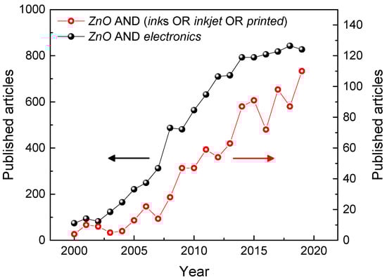
Figure 1.
Published articles from 2000 to 2019 on “ZnO” and “electronics” (closed black symbols), and on “ZnO” and “inks”, or “inkjet”, or “printed” (open red symbols). Data extracted from Scopus database on 20 March 2020.
The interest in the field of ZnO-based devices can be ascribed to its remarkable properties. ZnO is a semiconductor with a direct band gap value of 3.4 eV and a large exciton binding energy of 60 meV. ZnO crystallizes in the hexagonal wurtzite-type structure under ordinary conditions; the wurtzite structure of ZnO belongs to the space group P63mc. The synthesis of ZnO can be carried out in vapor or liquid phases, being extremely versatile in terms of the attainable morphologies [20], like nanorods [21], nanowires [22], nanospheres [23], nanotetrapods [24], 2D nanoflakes [25], and others. ZnO nanoparticles (NPs) have found immense applications in the sector of chemical sensors [26], due to their extremely large surface/area ratio, and are also reported as cytotoxic [27]. ZnO NP-based hybrids have also demonstrated to be effective nanocatalyst, with enhanced catalytic performance in comparison with other already reported systems [28]. By contrast, quasi-1D nanostructures have high piezoelectricity [29,30,31], electrochemical activity [32], remarkable biocompatibility, as reported by the Food and Drug Administration [33], suitability for cellular stimulation [34], intracellular sensing [32,35], and ease of surface functionalization [36].
From these outstanding physicochemical properties, it is clear that the possibility to print ZnO-based (nano)crystalline inks could be an important step for the integration of this material in the world of printed electronics devices [37]. This review aims to provide a critical and selected overview of the different ZnO-based ink formulations and printing approaches on solid surfaces from the last 15 years. The major applications of each printing technique will be investigated, with a focus on specific target applications, namely chemical and physical sensors, photocatalysis, solar cells, electronic devices, and other ones. The review is organized as follows. Section 2 deals with a brief introduction of the major printing techniques used for inks at different resolution (e.g., screen printing, flexographic printing, 3D printing, inkjet printing, and dip pen nanolithography). Section 3 summarizes the most relevant synthesis approaches for ZnO, focusing especially on wet chemistry approaches, considering their relevant role in the field of ink formulations. Section 4, Section 5, Section 6, Section 7, and Section 8 report on the application of different ZnO-based inks adapted for screen printing, flexographic printing, 3D printing, inkjet printing, and dip pen nanolithography techniques, respectively. Section 8 contains the Conclusions and Perspectives.
2. Printing Techniques: A Brief Overview
2.1. Screen Printing
Screen printing is among the most versatile and well-known printing techniques for printed devices fabrication [38]. The printing operation is carried out by spreading an ink paste across the screen by using a squeegee (rubber blade). The screen represents the mesh, normally made of porous fabric or stainless steel. This leads to a lower paste viscosity that, in turn, permits its spread through the substrate. The screen is peeled off, and the viscosity of the paste returns to the normal condition by passing the squeegee (Figure 2). The major factors that govern the process of the screen peel are the viscosity of the paste, the squeegee speed, the tension of the screen, the area of the print, and the snap-off distance between the screen and the sample. The capillary number (Ca) is typically used to represent the interplay of viscosity, surface tension and printing speed, and is defined as Ca= μU/γ, where μ is the ink’s viscosity, γ is the ink’s surface tension, and U is the printing speed (typically around ~1 mm·s−1). The screen printing process has been recently theoretically investigated by Kapur et al. [39]. They analyzed the importance of surface effects that take place when the printed liquid is pulled out of the mesh. Their model was validated against a wide range of model inks, demonstrating that the range of Ca involved in the screen printing process is common for all the printers and is of the order of 10, based on the typical ink viscosities of about 10 Pa·s, surface tension of 30 mN·m−1, and snap-off speed of 2 mm·s−1. For these reasons, the screen printing process is generally independent of many of the experimental set-up parameters.
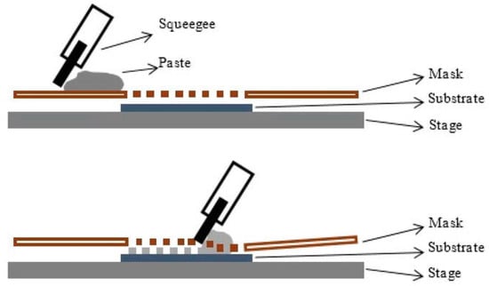
Figure 2.
Schematic representation of the screen-printing process, depicting a squeegee moving on the mask, allowing for patterned deposition of the paste on the substrate placed on a solid stage. Reprinted from Reference [41], distributed under the terms of the Creative Commons Attribution 3.0 License.
The typically employed inks cause the formation of a thick wet layer (10–500 μm), thereby resulting in thick films, which can be suitable for printing electrodes. The printing method is typically constrained by a low lateral resolution, typically hundreds of microns [40], and by the exposure of the ink to the atmosphere during printing. The critical aspect is to maintain the ink in a wet state whilst on the mask during the printing operation that can last several hours in case of industrial processes.
2.2. Gravure Printing
Gravure printing is among the most relevant technologies for the production of flexible and low-cost printed electronics, due to its high-speed, high-throughput, high-resolution deposition of functional materials and compatibility with roll-to-roll processes [42,43,44]. As depicted in Figure 3a, the technique relies on the transfer of ink from small engraved cells in the gravure cylinder to the flexible substrate in three steps: (1) filling (cavities are overfilled with ink by ink bath or chambered doctor blade); (2) wiping (removal of excess ink from the non-image areas using doctor blade); (3) transferring (the moving substrate contacts the free surface of the ink in the well, and ink is pulled from the well onto the substrate). The quality of the printing is governed by the wettability of the ink to the printing plate, doctor blade, and substrate [45]. These individual functions are linked by the capillary number. In order to realize high-resolution and high-fidelity processes, it is essential to accurately adjust the printing speed and pressure, ink viscosity, and surface tension. Moreover, the doctor blade angle and drying temperature can play a key role in the final print quality, as well as the engraved cylinder cell parameters such as tone, screen angle, line density, and stylus angle.
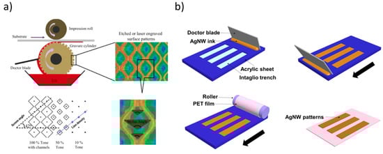
Figure 3.
(a) At the top, schematic representation of the gravure printing process, depicting engraved surface patterns. At the bottom, main parameters involved in the patterning process (tone, screen angle, line density and stylus angle). Reprinted from reference [45], Copyright (2013), with permission from Elsevier. (b) In the case of the inverse gravure printing, the patterns on a flat plate are transferred to the flexible substrate mounted onto a roller. Reprinted from reference [47] under a Creative Commons Attribution 4.0 International License.
To analyse and better understand the printing mechanism [46], Kitsomboonloha and coworkers introduced an “inverse direct gravure printing”, in which a flat plate is used to transfer patters to a substrate rather than using roll, allowing the direct imaging of the individual processes of filling and wiping. A resolution lower than 2 μm with a printing speed as high as ∼1 m/s was achieved. The interesting study from Huang and Zhu [47] pointed out the possibility to leverage this process to deposit inorganic conductive ink materials, such as silver nanowire inks onto flexible plastic substrates (see Figure 3b).
2.3. Flexographic Printing
Flexographic printing is a very popular printing technique which employs a flexible printing plate to deposit ink onto a receiving substrate [48,49]. As opposed to gravure printing, the ink in flexographic printing is transferred from a raised surface (relief printing) and not from carved micro cavities. The printing process can be described as follows. The inked plates bringing a raised image are wrapped around cylinders on a web press and rotate at high speeds for transferring the ink through small holes from the anilox roll to the substrate (Figure 4). The printing process can be adapted to different materials (e.g., paper, carton board, metal, flexible packaging), and is compatible with a wide range of inks, including water-based inks. The pattern length scale and the eventual triggering of finger instabilities by flexographic printing can be tuned by printing velocity, fluid viscosity, and surface tension, and normally lies in the tens of microns. For rigid printing plates, the printing quality mainly depends upon the capillary number Ca = vη/σ, where v is the meniscus velocity, and η and σ are the viscosity and the surface tension of the liquid, respectively. The optimal range of Ca is typically comprised between 10−3 and 1. In fact, Ca has to be smaller than 1 in order to make negligible the viscous friction and to preserve the ink shape under rotation flexographic printing. However, the smaller the Ca, the higher would be the wavelength of capillary fingering instabilities, as expressed by the equation λ∝Ca−1/2 [50]. For this reason, Ca should not be lower than 10−3, as reported by the same authors. Interestingly, in the case of elastic flexographic printing plates, an emerging role is played by the elastocapillary number, defined by plate elasticity and surface tension [50]. In particular, the extensional elasticity of the printed ink during the separation of the printing plate and the inked substrate can play an important role in flexographic printing. To this aim, it is possible to introduce the adimensional elastocapillary number to quantify the interplay between viscosity, surface tension, and elasticity in determining the possible instabilities of ink printing, as Ec = λEσ/ηl where λE is the fluid characteristic relaxation time for the elastocapillary thinning action, η is the shear viscosity, and l is the appropriate length scale for viscous instability. As observed by Morgan and coworkers [51], the increase of ink elasticity can greatly affect the uniformity of the printed pattern, decreasing the overall relative size of the printed finger features, as a consequence of the extensional elasticity on the ink filamentation during the separation of the printing plate and the inked substrate. Recent developments have allowed the engineering of nanoporous stamps made by carbon nanotubes (CNTs), permitting micrometer-scale lateral resolution and nanoscale thickness (about 50 nm) to be achieved [52].
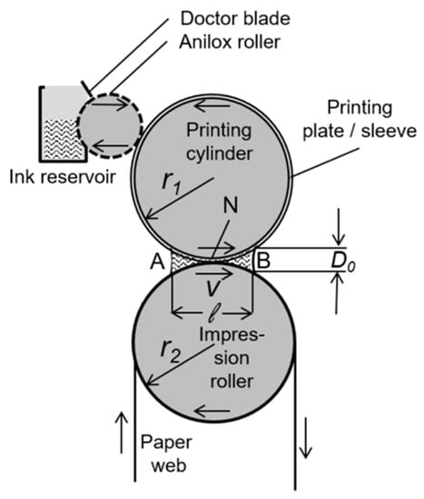
Figure 4.
Sketch of a flexographic printing unit. The zones A and B represent the incoming and outgoing ink meniscus, respectively, N is the printing nip, D0 is the meniscus height, ℓ is the width of the wetted zone. Reprinted from Reference [50], under the terms and conditions of the Creative Commons Attribution (CC BY) License (http://creativecommons.org/licenses/by/4.0/).
2.4. Three-Dimensional (3D) Printing
Three-dimensional (3D) printing, or additive manufacturing (AM), is an emerging manufacturing technology for the creation of customizable patterns in three dimensions, offering new opportunities for the formation of a new class of multifunctional nanocomposites [53]. This technology allows reconfigurable objects to be printed by means of computer-aided design (CAD) software, permitting the design and the 3D structure to be optimized in a sequence of layers (Figure 5). Three-dimensional printing is based on the extrusion of continuous filaments (inks) in a layer-by-layer sequence by using the CAD tools. This method allows the fabrication of structures with features typically at the microscale (0.1–100 μm) and mesoscale (>100 μm), as a function of the nozzle diameter. Notably, the ability to fabricate a variety of structures necessitates the control of the formulation and the rheological behavior of the inks and of the major printing parameters (e.g., velocity of the printing, pressure extrusion). Along with polymers and biomolecular systems, these techniques have been applied also for ceramics, by tuning process control, post-treatments, and energy source–material interactions [54].
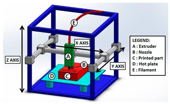
Figure 5.
Scheme of a representative fused deposition modeling (FDM) setup. FDM consists of an extruder (A), which allows the ink to be driven towards the nozzle (B) for the fluid ejection to form the printed object (C). The process is carried out by forming the printed item on a hot plate (D) to control the temperature and the resulting ink fluidity. The ink is generally a highly viscous fluid obtained by heating a thermoplastic material, and it is deposited through the extruder/nozzle system as a continuous filament of well-defined dimensions (E). Reprinted from Ref. [55] under the Creative Commons Attribution (CC BY) License (http://creativecommons.org/licenses/by/4.0/).
2.5. Inkjet Printing
Inkjet printing is among the most widespread micropatterning techniques in the context of ZnO inks due to its adaptability to inks with different physicochemical properties and the inherently low cost of the instrumentation. Inkjet printed droplets are typically in the 10–100 microns lateral scale range, being directly related to the nozzle size from which the droplet is ejected. During droplet formation, energy is distributed among viscous flow, drop surface tension, and drop kinetic energy [4]. In turn, this leads to a liquid jet resolving into a droplet hitting the substrate surface. This technique has been implemented mainly following the continuous inkjet (CIJ) printing, and the drop-on-demand (DOD) inkjet printing. In the CIJ case, the ink is subjected to a high pressure which forces it through the nozzle, resulting in a jet which breaks up into a stream of droplets through the Rayleigh instability. The droplets formed are electrically charged, so they can be properly guided by an external electric field. In the DOD approach, the droplets are generated only when required, by a series of pressure pulses inducing the droplet ejection when needed [56]. In turn, the DOD method can be divided, according to the mechanism of drop formation, into four subclasses, namely, thermal, piezoelectric, electrostatic, and acoustic [57]. The thermal and the piezoelectric jetting modes are the most employed. In the piezoelectric printing approach, the system employs a piezoelectric crystal, such as lead zirconate titanate (PZT). As the voltage is applied, the PZT piezoelectric transducer creates acoustic waves, forcing the ink out of the chamber through the nozzle, resulting in droplet formation (see Figure 6). Notably, it is possible to integrate the hardware with automated translation stages, allowing precise pattern placement and registration to prepare multilayered patterns with different materials. Inkjet printing has found many applications in the field of direct patterning of many different materials, such as colloidal silver nanoparticles [58], oil droplets [8], biomolecular systems [59,60,61].
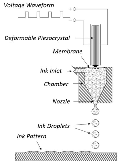
Figure 6.
Schematic illustration of piezoelectric inkjet printer. Diagram of the operation of a piezo drop-on-demand (DOD) ink-jet print head. The applied voltage waveform induces the piezocrystal deformation, which generates a pressure wave in the fluid ink inside the microfluidic chamber. The pressure pulse determines the formation of the droplets and their ejection through the nozzle onto the solid support for the pattern formation. Reprinted from Reference [62], Copyright (2004), with permission from Elsevier.
Notably, the rheological properties of the ink play a fundamental role in the printing process. Indeed, a careful optimization of the physicochemical characteristics of the ink is necessary. In this regard, a common strategy to evaluate the jettability of the ink formulation is by means of the Derby plot (see Figure 6), which illustrates the different regimes of inkjet printing by plotting the Weber number, We = (ρν2L)/σ, against the Reynold number, Re = (ρνL)/μ, where ρ is the liquid density, σ is the surface tension, L is the characteristic length scale, i.e., the droplet diameter, v is the velocity of the fluid, and μ is the dynamic viscosity of the fluid. Notably, the droplet diameter is usually similar or slightly larger than the size of the nozzle. However, some reports have shown that it is possible to reduce its size by adapting waveform [61] or by employing satellite printing [63].
The ideal ink composition lies within the “Printable Fluid” regime (green dot in Figure 7), whereas a fluid at low viscosity lies in the “Satellites” regime, due to the possibility of generating satellites upon jetting. Another commonly employed parameter that helps to predict the jettability of an ink, is the Fromm number (Z), which is defined as the inverse of the Ohnesorge number Oh = μ/(ρσL)0.5, i.e., Z = 1/Oh. For a fluid to be printable and to avoid the formation of satellites, this number has to be in the range comprised between 1 and 10. The ink rheological properties are generally tuned by adding additives such as glycerol, ethylene glycol, with the aim to increase the viscosity and also reduce the material aggregation within the nozzle microchannels. The high-throughput capability of the piezoelectric inkjet printing is among the most relevant features of this technology. In fact, in order to increase the printing speed, it would be possible to simultaneously use multiple nozzles, thereby enabling the inkjet printing technology for large scale industrial applications [64].
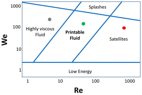
Figure 7.
Derby plot giving information on the fluid printability regimes as a function of Weber (We) and Reynolds (Re) numbers. The coordinate system illustrates the physicochemical combination of fluid properties that determine a good quality inkjet printing process. The area containing the red dot represents experimental conditions corresponding to satellite-forming inks, the grey dot labels the regime of high-viscosity inks, while the green dot represents a well-printable ink regime. At the lowest and highest values of We, the printability of the inks is generally reduced for lack of energy needed to induce the drop formation and ejection, and because of splashing phenomena after the impact of the drops with the solid interface, respectively.
2.6. Dip Pen Nanolithography
Among the available printing approaches, scanning probe lithography techniques constitute an important class of direct-write nanolithographic methods, enabling nanoscale material patterning, with resolutions below 10 nm, bypassing the diffraction limit. The first technique worth mentioning is dip pen nanolithography (DPN). The discovery of this method dates back to 1999, when the group of Mirkin leveraged an atomic force microscopy (AFM) tip as a “micro-pen”, a gold solid substrate as a “paper”, and molecules loaded on the tip as an “ink”, for the development of an innovative and direct-writing setup [65] (see Figure 8). In particular, the DPN printing process consists of the direct-writing of the ink solution, loaded on the probe, from the tip onto the support surface. The deposition of material occurs as the tip is mechanically brought in contact with the solid interface, leading to the formation of a spot on the surface. DPN allows for patterning a wide variety of materials, both soft and hard, with high accuracy and lateral resolution ranging from few microns to sub-100 nm [66]. It has been demonstrated to be a useful tool for patterning of a plethora of different materials, from biomolecules, to synthetic polymers, to inorganic materials [67]. In order to figure out the transport mechanism of patterning in DPN in depth, it is fundamental to consider that the deposition of material from the tip onto the surface is a complex process involving physicochemical phenomena both at molecules/tip and molecules/support interfaces.
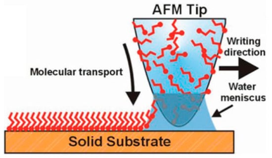
Figure 8.
Scheme of the mechanism for molecular ink deposition by dip pen nanolithography (DPN). The atomic force microscopy (AFM) tip loaded with the molecules to pattern is brought into contact with the solid substrate to induce the molecular transport process through the water meniscus in between the tip and the receiving surface. As sketched, molecules containing chemical moieties that strongly interact with the solid surface can be chosen, thereby inducing an ordered orientation of the chemical structures at the interface (e.g., self-assembled monolayers, SAM). Reproduced with permission from Reference [68] Copyright © 2019 WILEY-VCH.
First of all, it is possible to distinguish diffusive inks from liquid inks [67]. The former, also known as molecular inks, are characterized by a diffusion-driven transport mechanism of molecules from the tip to the surface. The deposition is carried out by dipping a bare probe into a well containing the ink of interest to load it on the tip surface. Then, the solvent evaporates leaving molecules physisorbed on the tip. As the loaded tip comes into contact with the support surface, a water meniscus forms and ink molecules diffuse towards the surface because of the concentration gradient. The tip-surface dwell time allows the spot size and the amount of deposited material to be controlled [68]. On the other hand, liquid inks are generally aqueous solutions that exhibit a transport mechanism mainly dependent on the bulk fluid flow, strongly affected by viscosity. They are kept in the liquid state over all the printing process and form dome-shaped features. In this case, the ink is loaded on the tip through capillary forces and it is deposited in liquid state on the support. As the liquid-loaded tip is in contact with the solid surface, a fluid flow arises and the transport of ink molecules to the surface can occur [68]. This flow is influenced by many parameters, including the Laplace pressure at the meniscus, the surface-free energy at the solid interface, and the ink dynamic viscosity. In principle, the formation of the water meniscus is not necessary for liquid inks to be deposited, but it is still present, therefore the composition of the released ink is affected by the relative humidity (RH) [69]. The resulting spot size is in the microscale. The experimental conditions are crucial for a successful and reproducible deposition in both transport mechanisms. The first factor to mention is certainly the RH in the deposition chamber, since it positively affects the ink transport on the substrate. The RH determines the spontaneous formation of the abovementioned water meniscus between the ink-coated tip and the substrate, a phenomenon which has been experimentally observed by environmental scanning electron microscopy (ESEM) [70], and which is fundamental for the material transport onto solid supports. Indeed, the increasing RH results in a larger water meniscus, which facilitates the ink deposition, especially in a diffusive mechanism. Another parameter increasing the transport rate is the temperature, which positively affects the fluidity of the ink, especially for liquid ones [68].
From a more technical point of view, it is interesting to notice the improvements also in terms of the architecture of the surface patterning tools (SPTs), which consist in the cantilever/tip system used for the deposition. As mentioned, the simplest SPT consists of an AFM-tip, but innovative architectures have also been developed. In this context, the micro-cantilever spotting (µCS) is a relevant example, as it shows the combination of the microfluidic fabrication technology with the DPN patterning tools [71,72]. More specifically, a µCS consists of a sharp tip crossed by a microfluidic channel, which constantly delivers liquid to the tip edge. This system offers the possibility to continuously refill the tip edge avoiding ink re-loading steps. Finally, it is important to highlight that printing speed and multiplexing capability, which represent the main DPN limitations, can be overcome by the use of multi-tip devices. In fact, DPN has been implemented for the multiple deposition of different chemicals, sequentially or in parallel, showing high multiplexing potentiality. Polymer pen (PP) represents a relevant example of DPN multiplexing [73]. It combines DPN and microcontact printing (µCP) features, by using an array of soft elastomeric tips (~106 pyramid-shaped tips), that can be brought into contact with the solid support and optically leveled for uniform patterning. Additionally, the possibility to control the relative position of the tip array with respect to the support by tilting has been demonstrated to be a powerful way to print gradient patterns of molecules [74]. A summary of the different printing methodologies reported in this review can be found in Table 1, which specifically lists ink properties, such as viscosity and surface tension, printing resolution, and process characteristics (speed, resolution range, typical thicknesses, etc.).

Table 1.
Main features of the printing methods relevant for ZnO-based inks printing reported in this review.
3. Zinc-Based Materials: Towards New Rational Synthesis
ZnO Synthesis Approaches
ZnO synthesis can be carried out by physical, wet chemistry, or biological approaches. For the development of ZnO inks, wet-chemistry based synthetic approaches are the most common [75,76,77,78]. Typically, ZnO NPs are synthesized by direct precipitation method using water-soluble zinc salts, such as zinc nitrate or zinc acetate, and alkaline agents, such as NaOH or KOH, as precursors. Usually, the result of the synthesis consists in the formation of a precipitate that is afterwards washed and calcined (400–500 °C) to obtain ZnO NPs with the desired morphology and crystallinity characteristics. A typical example of reaction used for the synthesis of ZnO NPs starting from zinc acetate precursor in the presence of a basic amine is the following:
Zn(CH3COO)2 → Zn2+ + 2 CH3COO−
R-NH2 + H2O → R-NH3+ + OH−
Zn2+ + 2 OH− → Zn(OH)2 → ZnO + H2O
Conversely, the synthesis of ZnO 1D materials by wet-chemistry is more challenging, especially as concerns their application in electronics, as well as their full integration into devices. In fact, conventional wet-chemistry synthetic methods for ZnO nanowires (NWs) typically lead to poor reproducibility, low density, and low length (few microns) [79]. A typical growth of ZnO in an equimolar zinc nitrate–hexamethylenetetramine (HMTA) solution, as discussed in detail by Zainelabdin et al. [79], involves the reactions:
(CH2)6N4 + 6H2O → 4NH3 + 6HCHO
NH3 + H2O → OH− + NH4+
Zn2+ + 2OH− ⇄ Zn(OH)2 ↓
Zn(OH)2 → ZnO + H2O
The role of HMTA is to decompose into ammonium ions, that can complex Zn ions (which are provided by the water-soluble zinc salt), and into OH−, that drive the formation of zinc hydroxides, and finally zinc oxide [22]. A detailed analysis of the solution chemical speciation of these precursors in presence of an aluminum substrate to form Zn/Al( layered double hydroxides was discussed in a paper by some of the present authors [80]. In a previous work, our group reported on a wet-chemistry fabrication method of ZnO NWs conceived by means of a rational design [81,82,83]. Numerical modelling was employed to find the optimal concentration of ethylenediamine (EDA), a zinc-binding molecule that permits to grow thin NWs at alkaline pHs and in presence of chloride ions to favor the stabilization of top-face of NWs. Notably, EDA is produced by the less harmful monoethanolamine (MEA). More specifically, as shown in Scheme 1, in the nutrient growth solution, Zn ions form complex species with ligands (i.e., ZnL, in which L is a generic zinc ligand molecule), which, in turn, can form a complex with the alcohol through association with one of the two unshared pairs of electrons of the oxygen atom (1), thus increasing the possibility that a good nucleophile, like ammonia, can displace the hydroxyl leaving group and forms EDA (2, and 3). Finally, the hydroxylated form of zinc complex gives back the initial ZnL specie (4) (see Scheme 1). The EDA formed in situ can modify the speciation of zinc in the nutrient growth solution employed for the synthesis of ZnO NWs (see Figure 9) by producing at pH 8.9–9 the species [Zn(EDA)2]2+ which is able to control the precipitation of ZnO by slowing down the homogenous growth in solution, and favoring the growth of ZnO NWs. This approach permits ZnO NWs to be produced with densities >8/μm2, record length (>15 μm), and aspect ratio (>200) onto flexible substrates.
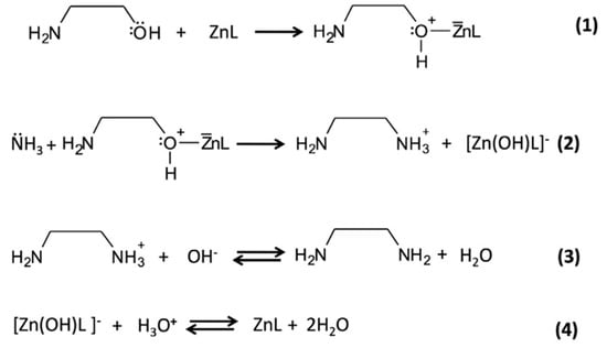
Scheme 1.
Formation of ethylenediamine (EDA) from monoethanolamine (MEA) in the presence of zinc ions forming complex species.
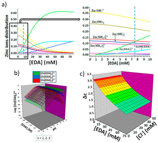
Figure 9.
Rational approach for the ZnO synthesis by reporting the ethylenediamine (EDA) assisted control on zinc speciation. (a) Effect of EDA concentration on the zinc ions distribution (b) Combined effects of EDA concentration and pH on the formation of complex species between zinc and EDA and (c) Combined effects of EDA and chloride ions concentration on the degree of supersaturation. Reprinted from Reference [82], Copyright (2018), with permission from Elsevier.
The synthesis routes reported above briefly account for the preparation of ZnO NPs and NWs, which are commonly used for ZnO inks based on the stable dispersion of ZnO nanomaterials. However, as far as inkjet printing is concerned, possible agglomeration of particles in the ink may cause clogging of the nozzles, thereby limiting the choice of particle size and nozzle diameter as well as that of ink concentration and viscosity [3,84]. In order to mitigate NP agglomeration, ink mixtures are often constantly agitated or surfactants are added to maintain the particles in dispersion. As an effective alternative to overcome such drawbacks, a different approach can be adopted. This consists in printing solution-based precursors containing zinc salts (e.g., zinc acetate and zinc nitrate), to obtain ZnO precursor patterning instead of printing already formed ZnO NPs. In this regard, in the same year Lloyd et al. [85] and Kwon et al. [86] reported on flexographic printing and inkjet printing, respectively, of Zn acetate precursor ink patterns to achieve selective hydrothermal ZnO local growth. In more recent works, Güell et al. [87] and Zhang et al. [88] reported on spatially controlled growth of ZnO nanowires and nanorods, respectively, by printing Zn precursor inks based on zinc nitrate. In all cases, thermal decomposition of the dried Zn precursors was leveraged to form a seed layer of ZnO nanocrystals for the growth of ZnO NWs [89]. Zinc acetate decomposition is a multistep process, as comprehensively reported in previous works [90,91]. Briefly, after dehydration, anhydrous zinc acetate decomposes at a temperature of about 237 °C to form basic zinc acetate from the loss of acetic anhydride:
Above 300 °C (300–330 °C) basic zinc acetate decomposes to its oxide due to decarboxylation, leading to the formation of Zn nanocrystallites:
Thermal decomposition of zinc nitrate based precursor inks to form ZnO NP seeds can be more simply summarized as follows [91]:
In Reference [87] this reaction was completed at 450 °C to form ZnO nanocrystallites.
4. ZnO-Based Screen-Printed Devices
Screen printing, due to its large processing capability and high throughput, is vastly used for the production of low-cost and sustainable electronic devices, such as transistors, solar cells, varistors, sensors, etc. Ismail et al. studied the structural properties of screen-printed ZnO thick films on glass followed by annealing [92]. Inks were formulated from ZnO and zinc chloride powder mix with the addition of propylene glycol as a binder, while the viscosity was adjusted by paraffin. Printed films were reported to have granular porous morphology, with roughness within 100–200 nm, and no specific crystallographic orientation. It is believed that the grain size and pores of the films affected electrical properties. Suchat et al. compared ZnO screen-printed films with films obtained by spray pyrolysis [93]. The screen-printed ZnO thin films showed an amorphous morphology and low percentage of transmittance in the visible range and slightly higher sheet resistance in comparison to films obtained by spray pyrolysis (about 100 Ω square−1 vs. 90 Ω square−1). These findings clearly paved the way for the use of screen-printed films in solar cells and sensing applications. Indeed, Zargar et al. demonstrated an example of using a ZnO ink to print films for antireflection coating of solar cells [94]. They used an ink formulated with ZnO powder and ZnCl2, with ethylene glycol as a binder. X-ray diffraction (XRD) and scanning electron microscopy (SEM) characterizations revealed that the printed films, annealed at 550 °C, had a polycrystalline structure and consisted of agglomeration of small crystallites to form spindle-, dumb bell-, and cuboidal-shaped particles and fused clusters. The dark direct current (DC) conductivity measurements detected a significant activation energy of 0.27 eV, suggesting that the conduction process of charge carriers was thermally activated. Hence, screen-printed films were suitable for optoelectronc devices and solar cells. Sarkar et al. investigated the use of diblock copolymers in ink formulation, in order to direct the shape and morphology of metal oxide nanostructures in thin films, where the sol–gel-based metal oxide formation was combined with the assembly of hydrophilic metal oxide precursor sols within the hydrophilic domain of self-assembled amphiphilic diblock copolymer mesophases [95]. They further investigated this approach in order to obtain several-micron-thick films containing tailored ZnO nanostructures required for dye-sensitized solar cell (DSSC) applications [96]. In their work, the sol–gel solution was first used to synthesize ZnO NPs of different sizes, which were then used to prepare the screen-printing paste containing poly(styrene-block-ethylene oxide) polymers. The ZnO nanoparticles were presynthesized by a sol-gel route and then added to the pastes for screen printing at different weight fractions of the ZnO precursor and characterized by XRD, optical microscopy and SEM, revealing their crystallinity and granular morphology (see Figure 10). Subsequently, the authors leveraged the screen-printed ZnO prepared films for preparing dyes sensitized solar cells with good performances, in particular obtaining a power conversion efficiency of 0.71% for a single printed layer containing 0.075% of zinc precursors.
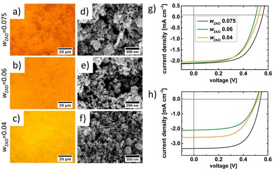
Figure 10.
Applications in dye-sensitized solar cells (DSSCs): (a–c) optical microscope images and (d–f) SEM images of screen-printed films prepared from pastes obtained from sol-gel ZnO nanoparticles using 0.075, 0.06, 0.04 weight fractions of the ZnO precursor respectively. (g,h) J–V characteristics for DSSCs fabricated from different ZnO nanoparticles-based pastes with two different film thicknesses of the active layer. Reproduced with permission from Reference [96] Copyright 2015, WILEY-VCH.
Such a formulation approach allows screen printing for DSSC production, and can also be extended to other inorganic semiconducting materials that follow the diblock-copolymer-assisted sol–gel synthesis approach. One of the main challenges of screen-printing is to obtain good compaction of the films. To improve the film compaction De La Rubia Lopez suggested preparing inks from the mixture of 60% powder by 95.5 mol% ZnO, 1.5 mol% Sb2O3 (or Zn7Sb2O12 orthorhombic spinel phase.), 0.5 mol% Bi2O3 (or Bi38ZnO58 sillenite phase), 0.5 mol% Co3O4, 1.25 mol% NiO, and 0.75 mol% MnO, with 40 wt.% of organic vehicle, comprising terpineol, ethylcellulose, and [2-(2-butoxi-etoxi-ethyl)] [97]. They showed that inks with spinel and sillenite phase produced thick films with high density exhibiting varistor properties with good electrical response after being annealed at 900 °C, whereas annealing at higher temperatures led to Bi volatilization and its removal from the varistor microstructure due to high area-volume ratio.
Electrolyte-gated transistors (EGTs) have attracted great interest for flexible electronics and biosensing applications over the last decade because of the large capacitance of the electrolyte, which allows charge accumulation into the semiconductor at low gate-source voltages, and high sensitivity to the ionic species that may contact or exist in the electrolyte. Carvalho et al. demonstrated fully printed and flexible EGTs on paper and glass, based on an interconnected ZnO nanoparticle matrix, arranged in a staggered-top gate architecture [98]. In their work, ethyl cellulose (EC) was empoyed as a binder in the developed ink to disperse ZnOs, thereby providing the necessary rheological properties for screen printing and good layer formation at a maximum annealing temperature of 150 °C. These devices exhibit low operation voltages, with a subthreshold slope of 0.21 V dec−1, a turn-on voltage of 1.90 V, saturation mobility of 0.07 cm2 V−1 s−1, and an Ion/Ioff ratio of more than three orders of magnitude. Further investigation into sustainable and eco-friendly ink formulations may allow fabrication of electrolyte gating for transistor-based technology. Nanostructured ZnO is also a known as a chemoresistive and ultraviolet (UV) light-sensing material [99,100]. Recently, Manjunath et al. suggested preparation of thixotropic pastes by mixing solution combustion synthesized ZnO powder as a functional material with a Na-carboxy-methyl cellulose binder in water, in order to fabricate a gas sensor for ammonia, ethanol, Cl2, H2S, and liquefied petroleum gas (LPG) [101]. They revealed that non-stoichiometric, phase pure, and adhered thick films with optical band gap around 3.17–3.25 eV conferred gas sensing properties due to the recombination of electron–hole pairs at intrinsic defects. ZnO films obtained from glycine-fuel system showed a high response to UV irradiation for exposing time of 90 s, and exhibited good gas sensitivity of ~8, 5, 3, and 10 at operating temperatures of 50, 100, 200, and 100 °C while being exposed to 100 ppm of NH3, C2H5OH, Cl2, and 50 ppm of H2S, respectively, with faster response and recovery speed. In turn, high sensitivity of ~6 was obtained with 100 ppm of LPG at 350 °C in ZnO films from citric acid fuel-system. Such results clearly indicate that dual-function sensors can be fabricated by carefully tailoring the ZnO ink formulation. Another example of a screen-printed UV photodetector was demonstrated by Figueira et al. by screen printing ink using ethylcellulose as a binder and 80:20 toluene/ethanol solution as a solvent [102]. Films were printed onto a flexible cork sheet substrate into top-electrode architecture using mild temperatures. Such devices allowed for a fast response to UV irradiation, with a τrise < 5 s and τfall < 2 s, which remained stable for more than one month without any encapsulation or special storage conditions. The findings suggest that eco-friendly ink combined with low-cost and sustainable cork substrate represents great potential for wearable applications.
5. ZnO-Based Gravure and Flexographic Printed Devices
Some reports have investigated the possibility to realize ZnO thin films by gravure printing for applications in organic solar cells (OSCs). In this regard, Vilkman et al. [103] developed a ZnO nanoparticle ink that could be used as a hole-blocking layer in inverted P3HT:PCBM OSCs. The authors demonstrate the possibility to achieve a good power conversion efficiency (PCE) of 2.9%. In an excellent work, Zhang et al. used gravure printing [104] to deposit high-quality ZnO thin film as the electron transport layer (ETL) for P3HT:PCBM-based and PTB7-Th:PC71BM-based inverted OSCs. They optimized the ZnO film deposition by gravure printing by tuning the web tension and the printing parameters (the web speed is fixed at 0.2 m/min, and the printing roller speed is controlled at specified values between 0.6 and 2.4). The authors found that it was possible to obtain a very uniform thin film (about 50 nm in thickness) by increasing the printing roller speed up to 2.4. The PCE of the resulting P3HT:PCBM-based device is similar to the spin-coated ZnO thin film as the ETL, being 2.4% and 2.8%, respectively.
Some applications of flexographic printed ZnO devices can be found in the field of sensors. In particular, Lloyd et al. [85] used flexographic printing to deposit zinc acetate precursors on silicon/polyamide substrates to form ZnO seeds for the growth of ZnO NWs by wet chemistry. Importantly, the authors demonstrated the possibility to achieve printable line of <60 µm in width. The resulting ZnO NWs (diameter between 40 and 60 nm) were characterized by energy-dispersive X-ray spectroscopy and using XRD, showing a 1:1 (zinc to oxygen) stoichiometric ratio and a remarkable c-axis crystal orientation, highlighting the high-quality crystalline structure. The authors leveraged these interfaces for the realization of a resistive sensor for oxygen. A more insightful application in the field of sensing was provided in the study of Assaifan et al. [105] who developed non-faradaic biosensors based on electrochemical impedance spectroscopy (EIS) to detect the pp65-antigen of the human cytomegalovirus. The authors optimized the fabrication of a ZnO nanotexturing of the film surface through a 150 °C drying process between multiple prints of zinc acetate precursor. They characterized the obtained films by a series of techniques (XRD, X-ray photoelectron spectroscopy (XPS), SEM, and AFM) to verify the conversion to ZnO. The ZnO surface was functionalized with antibody for the pp65-antigen by standard (3-aminopropyl)triethoxysilane (APTES)/ glutaraldehyde chemistry, finally obtaining a low limit of detection of 5 pg/mL (see Figure 11).
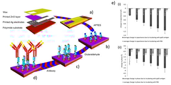
Figure 11.
Applications in EIS sensors. Schematic illustration of the printed biosensor (a) and its fabrication, and of the functionalization steps (b) covalent linkage of (APTES) to ZnO, (c) modification of APTES layer with glutaraldehyde, (d) antibodies linkage via aldehyde groups of glutaraldehyde. (e) Biosensor pp65-antigen sensing recorded in presence/absences of pp65-antigen in phosphate-buffered saline (PBS) at 50 mHz (i) change in capacitance and (ii) change in phase. Reprinted with permission from Reference [105]; Copyright 2016 American Chemical Society.
6. ZnO-Based Formulations for 3D Printing
Three-dimensional printing methodologies have also been applied for the direct fabrication of ZnO-based structures at the micronscale. Tubìo et al. designed ZnO inks suitable for such deposition techniques [106] by combining ZnO powder (0.7 microns size) 44–52 wt%, ammonium salt of poly(acrylic acid)(PAA) (Darvan 821A) 2 wt%, a viscosifier agent (hydroxypropyl methylcellulose, HPMC) 0.074 wt%, a gelation agent poly(ethylenimine, PEI, MW = 2000) 0.1 wt%. The authors found that the additives allowed to stabilize the ink against sedimentation. They characterized the ink rheology, highlighting a remarkable pseudoplastic behavior in accordance with the power-law model (shear-thinning) behavior, in which the apparent viscosity decreases with the increasing of the shear rate. The inks had excellent printing characteristics for the 3D printing process, as they could realize uniform and well-shaped lattices, resulting from the high quality of the ZnO ink (48 vol%). A further improvement of the mechanical strength was obtained by sintering the structures at temperatures between 900 °C and 1500 °C, reaching a compressive strength up to 11.09 MPa. In a more recent report, Som et al. developed a 3D-printed architecture reporting on ZnO-based hierarchical structures for enhanced photocatalytic performance [107]. They formulated a ZnO ink based on 20-40 nm sized ZnO NPs. These were combined for obtaining mixture of 50 wt% ZnO NPs (20–40 nm size) and 50 wt% ABS (acrylonitrile butadiene styrene). After sonication, the resulting resin was used to make the filament for 3D printer using an extruder at 210 °C. After that, they used the fused deposition modelling to obtain a 3D-backbone structure by using the extruded filament. In the subsequent steps, ZnO NPs were dip-coated on the 3D-backbone in order to produce a seed layer that was subsequently used to synthesize ZnO nanorods (NRs) or ZnO nanoflowers (NFs). The synthesized structures were then characterized by transmission electron microscopy (TEM) and XRD, and their photocatalytic properties were tested by degradation of the organic pollutant methylene blue, which was monitored by ultraviolet–visible (UV–Vis) spectroscopy. Intriguingly, Som et al. observed that the methylene blue dye solution was most rapidly degraded by the ZnO NF hierarchical structure on the 3D-backbone (methylene blue was completely decomposed after about 120 min), in comparison to the ZnO NRs, as more reactive photocatalytic performance is related to a large active area which allows for a more activated photocatalytic reaction (see Figure 12).
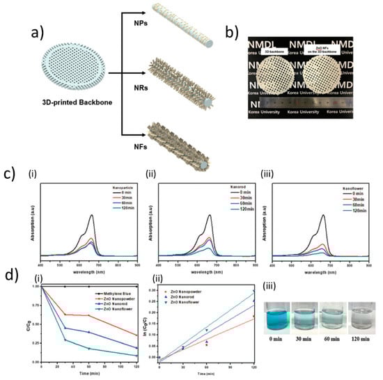
Figure 12.
Applications in photocatalysis. (a) Schematic representation of ZnO nanoparticles (NPs), nanorods (NRs), and nanoflowers (NFs) on the 3D backbone and (b) images of the 3D backbone (ABS + ZnO) and ZnO-NFs hierarchical structure on the 3D-backbone. Degradation of methylene blue (MB) dye solution. (c) Ultraviolet–visible (UV–Vis) absorption of MB photodegraded by ZnO (i) NPs, (ii) NRs, and (iii) NFs on 3D-backbones. (d) Graphs showing the (i) kinetics of methylene blue degradation and (ii) pseudo-first order rate constants of time. The photographs in (iii) show the MB degradation by ZnO-NFs on the 3D backbone. Reproduced with permission from the Royal Society of Chemistry, from Reference [107]; permission conveyed through Copyright Clearance Center, Inc.
7. ZnO-Based Formulations for Inkjet Printing and Related Devices
Inkjet printing represents among the most investigated printing approaches and, in fact, many studies deal with the application of this technique for the fabrication of a wide plethora of devices. Some recent studies have reported on inkjettable ZnO-based formulations, and fabrication of patterned ZnO films onto solid surfaces. In this regard, it is important to cite the in depth investigation of the physicochemical parameters governing the jettability of ZnO based inks carried out by Sharma et al. [108]. They showed a robust synthesis method by a top-down wet milling route to obtain ZnO NPs in the range comprised between 75 nm and 150 nm. Subsequently, they tested the jettability of different ZnO inks based on mixtures with glycerol and ethyleneglycol, thereby finding optimal values for inks based on ethyleneglycol that were characterized by a Z-number between 1 and 10. These inks also showed good colloidal stability against sedimentation up to a month.
Similarly, Gebauer et al. developed inkjettable inks for metal oxide NPs (ZnO, TiO2, CuO, SnO2, and In2O3), with high crystallinity and narrow size distribution, fabricated by chemical vapor synthesis [109]. These NPs were stable (maintaining their lateral size constant at about 20–40 nm) for about 200 days in ethyleneglycol; their stability was also confirmed by DLVO simulations. The resulting ZnO ink was printable by a commercial inkjet printer device onto Kapton and silicon surfaces. Another interesting example is from Suganthi et al. [110]. They prepared ZnO NPs by precipitation (particle sizes ranging from 15 nm to 40 nm). The particles were then used to prepare inks based on ethyeleneglycol. The minimum concentration of ZnO NPs to obtain continuous films was equal to 4%. Interestingly, they observed that the ink viscosity was decreased by the presence of the ZnO NPs, as a result of the formation of hydrogen bonds between the NPs and the glycol molecules, and disturbance in the native hydrogen bonding network of glycol. Research has also focused on printing ZnO seeds by using soluble precursors constituted by zinc acetate, or directly by ZnO NPs. Both methods allowed to achieve seed layers usable for the subsequent synthesis of ZnO NWs. For example, Kitsomboonloha et al. [91] produced inkjet-printed spots containing patterned zinc acetate precursors that were converted into ZnO crystallites which, in turn, permitted the growth of ZnO NWs in a bath containing zinc acetate and HMTA. The authors demonstrated the possibility to control the width (0.1–1 µm) and the length (up to 10 µm) of the ZnO NWs simply by tuning the concentration of the zinc acetate precursor (0.1–1 M) and the reaction time (up to 20 hours). Kwon et al. [86] characterized the effect of temperature on the size of printed seed layer spots of zinc acetate grown onto silicon or glass wafers. They observed that the substrate heating (room temperature, 30 °C, 40 °C, 50 °C, 60 °C, and 70 °C) permits the drying rate to accelerate, and increases the contact line receding rate. The receding contact line leads to a smaller pattern that, in turn, leads to a reduced size of the grown ZnO nanowire array (1 to 3 μm, with 100 to 150 nm in diameter). Alongside the control on the lateral size of the seed layer, the authors demonstrated preliminary applications as n-type accumulation device and UV sensor. Tsangarides et al. used zinc acetate seed printing to produce ZnO NWs (2–4 µm in height, and 300–600 nm in width) onto silicon surface. They demonstrated the possibility to finely control the thermocapillary effects by increasing the temperature of the substrate during inkjet printing up to 60 °C, finally allowing the uniform coverage of the printed spots or of continuous printed lines [111].
Many reports also show the possibility to directly formulate ZnO NP inks. For instance, Ko et al. demonstrated the possibility to print ZnO NP dispersions onto flexible substrates [112], in order to produce a low-temperature (<95 °C) process for the growth of high-aspect ratio NWs (>100). Precisely controlled patterns at the micronscale were obtained by Laurenti et al. who compared photolithography and inkjet printing [113] for the ZnO seed layer patterning. Intriguingly, they found that in both cases well-aligned ZnO NWs with hexagonal section were grown. The XRD measurements showed that highly c-axis oriented NWs were obtained on both kinds of patterned seeded substrates. However, Raman spectroscopy revealed that the NWs grown on the inkjetted seeds had more defects in comparison to those grown on the seed layer patterned by photolithography. The authors ascribed this result to the lower thickness of the seed layer at the borders of the patterned areas. Güell et al. [87] compared the crystal quality of ZnO NWs grown by a catalyst-free vapor–solid (VS) process at 900 °C onto Si or SiO2/Si substrates seeded with ZnO thin films prepared by conventional reactive sputtering or inkjet-printed patterned precursor islands. By means of high-resolution TEM (HRTEM), Raman, and microphotoluminescence characterizations, they demonstrated that the ZnO NWs by the inkjet-printed islands had a better quality in comparison to those obtained on the thin film seeding layer. In particular, the three techniques consistently indicated a reduced structural quality and a more pronounced tensile stress for the NWs grown on the thin film seeding layer, with the Zn precursor islands being more effective seeds in promoting the growth of strain-free ZnO NWs. As a matter of fact, a worsening of the crystal quality is expected as the thickness of the seeding film is reduced [113,114], and we can reasonably guess that the differences reported by Güell and coworkers could be reasonably ascribed to the very thin (about 150 nm in thickness) ZnO sputtered seed film. Sun et al. characterized the effect of the temperature of the receiving indium tin oxide (ITO) substrate on the morphology of the ZnO NWs grown onto printed zinc acetate ink seed layer [115]. At high temperatures (60 °C), the resulting seed layer was homogeneous, whereas lower temperatures (20–40 °C) triggered coffee ring effects. Interestingly, the ZnO NWs grown on the homogeneous seed layer exhibited a higher field emission property, showing a lower turn-on field (Eto = 3.6 V/μm) than those with coffee rings (Eto = 4.7 V/μm), where Eto is defined as the field at the emission current density of 10 μA/cm2. The authors explained this effect as a consequence of the redistribution of the seed layer grains on the printed spot.
A recently intriguing example of the versatility of inkjet printing of ZnO inks has been shown by Cook et al. [116], who prepared a colloidal ZnO quantum dots (QDs) ink suitable to be printed onto graphene films deposited by chemical vapor deposition (CVD) grown on Si/SiO2. The result was a pixelated photodetector that was characterized at different wavelengths in the ultraviolet− visible− near-infrared spectra, obtaining a remarkable responsivity of 97.5 A/W (24.4 A/W·V), and an external quantum efficiency (EQE) of 35580%. The authors compared these devices with the standard ZnO/PbS/graphene tandem structure, and observed that the pixelated inkjet-printed photoconductor ZnO showed higher responsivity and faster response time in comparison to the standard tandem technology. They ascribed this result to the inefficient charge transfer between different QD layers in the standard tandem structure. In addition, a great advantage of the inkjet-printed systems is the lower cost of fabrication, along with the compatibility to current conventional complementary metal oxide semiconductor devices (Figure 13).
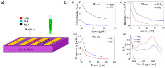
Figure 13.
Inkjet-printed ZnO-based photodetectors. (a) Schematic representation of printing of ZnO quantum dots (QDs), PbS QDs, and FeS2 NCs on graphene channels confined by Au electrodes on SiO2 (500 nm)/Si substrates. (b) Photoresponsivity as a function of power is depicted in (i), (ii), and (iii) along with the normalized spectral curve shown in (iv). As evident, the best performances were obtained by the ZnO-based QDs. Reprinted from ref. [116] Copyright 2019 American Chemical Society.
ZnO-based inks can be leveraged also for important applications in the field of strain sensors, given the outstanding piezoelectrical properties of the ZnO NPs [117], which have also been very recently used in inkjet printed graphene-cellulose electrodes [118]. For instance, Hassan et al. [119] investigated upon the realization of graphene flakes/ZnO composite inks to be inkjetted onto a micro-random ridged-type polydimethylsiloxane (PDMS) substrate. They leveraged the microridges on the PDMS to fabricate the cracks that are needed to produce the piezoresistive effect in the composite material. Interestingly, they observed that the optimal sensitivity of the resulting strain sensor was obtained at a graphene flakes/ZnO NPs ratio equal to 1:0.5, as a result of the optimal composite morphology at the micronscale. The strain sensor was characterized as a wearable bending sensor for finger motion detection (Figure 14). In a more recent work, Gardner et al. engineered an Al-doped ZnO (AZO) inkjet-printed piezoelectric field-effect transistor (FET) array to realize a pressure gradient mapping device. Albeit not providing details about the ZnO ink, they thoroughly characterized the pressure sensor [120], and discovered that it exhibited a linear I-V curve, indicating that each node acts as a resistor in absence of mechanical strain. The application of strain imposed an increase of current, that was quantified to be in the tenths of nA, and by gradually increasing the pressure the current grew proportionally.
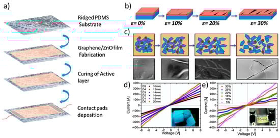
Figure 14.
Applications in strain sensors (a) Schematic representation of the fabrication steps for the ZnO/PDMS strain sensor. (b) Schematic explanation of the phenomenon that shows the tracks to remain conductive for large deformations under 0%, 10%, 20%, and 30% stretching. (c) Schematic explanations of the active layer over substrate with roughness of r = 0.34. On stretching, the gap changing between graphene flakes are increased, and then the electrical resistance of composite film is also increased. (d) Current-Voltage curves under bending with different diameters of strain sensor. (e) I-V curves under different stretching. Reprinted from Ref. [119] Copyright (2018), with permission from Elsevier.
For many years, ZnO has also proven of paramount importance as an effective platform for chemical sensing and UV radiation detection, and, in turn, many applications based on ZnO inkjet printing have been triggered in these fields. In a seminal work by Shen et al. [121] ZnO inks were prepared by sol-gel techniques and were printed using a commercial printer to fabricate gas-sensing thin films. Interestingly, they found that by changing the film thickness (i.e., the number print repetitions), the film morphology and electrical properties could be changed. Similarly, the effect of Pd, Ag, and ZrO2 dopant inks on resistivity and sensitivity was evaluated. Response curves were measured to 180 ppm acetone vapor at operating temperatures between 300 °C and 450 °C. For all the evaluated dopants, the measured sensitivity was more than doubled with respect to the non-doped printed ZnO thin films, with the maximum effect observed if the dopant ink was printed over the pure ZnO thin film. A gas-sensing platform to oxidizing gases (namely, NO2) based on ZnO NRs selectively grown on a well-defined inkjet patterned seed layer was developed by Chang et al. [122]. The fabricated gas sensor could respond to 750 ppb NO2 at 100 °C. A colloid ZnO NP solution served as the seed solution, inkjet printed by a custom-made inkjet deposition apparatus. A vertical jetting trajectory and straight ligament were achieved by adding 1% surfactant, and the resulting surface tension and viscosity of the seed solution were 22 mN/m and 1.1 cps, respectively. In a further work, Ryzhikov et al. [123] reported on improved tunable gas-sensing selectivity to different reduction gases (namely, CO, C3H8, and NH3) by means of ZnO thin films featuring different morphologies, printed with ZnO inks containing NRs, isotropic NPs, or cloud-like (CL) structures synthetized by an organometallic route. In the challenging field of chemosensors for NH3 diagnostic of breath analysis, Wu et al. [124] very recently formulated a graphene-ZnO functional ink for the development of a sensing platform integrated onto miniaturized complementary metal–oxide–semiconductor (CMOS) microhotplates (μHPs) via inkjet printing. ZnO and graphene synergistically contribute to an amplified responsivity compared to that by pure ZnO. Inkjet deposition provided a high-precision, material-efficient, and scalable technique, as well as excellent device-to-device reproducibility. The authors optimized active material and ink formulation, and developed an unprecedented temperature modulation algorithm which allowed to outperform conventional NH3 sensors in many aspects such as reproducibility, performance, power consumption, recovery time, and responsivity. Graphene-ZnO inks with different graphene loadings were directly printed onto the Au interdigitated electrodes (IDEs) of the CMOS μHPs (Figure 15a,b). Interestingly, polyvinylpyrrolidone (PVP) was used to both improve liquid-phase exfoliation (LPE) and stabilization of the ink precursors, and it also improved wetting and jetting properties of the inks. In order to remove PVP after deposition, the graphene-ZnO films on the μHPs were annealed at 400 °C for 2 h in Ar atmosphere. SEM images showed that film morphology significantly changed after annealing, with enhanced areas of exposure for the ZnO NPs and LPE graphene flakes. Device response to NH3 was dramatically enhanced by means of a temperature modulation scheme, showing (in pure NH3) responsivity of 1500% at 10 ppm, sensitivity of 125%/ppm, almost zeroed baseline drift, fast response and recovery times (τres of 28 s and τrec of 43 s, respectively), a signal to noise ratio of 5600, and excellent reproducibility (Figure 15c). Another important application of inkjet-printed ZnO based chemical sensors is by Beduk et al. [125], who developed a paper-based all inkjet-printed poly(3,4-ethylenedioxythiophene) polystyrene sulfonate (PEDOT:PSS)/ZnO sol-gel hydrazine sensor. They printed three layers of PEDOT:PSS on commercial paper, followed by two layers of ZnO sol-gel, and finally one layer of Nafion to encapsulate the sensing area (Figure 15d). ZnO treatment enhanced surface area by increasing roughness (Figure 15e). The crystallinity of the ZnO layer was demonstrated by XRD analysis of the ZnO modified PEDOT-PSS electrode (Figure 15f). The sensitivity toward hydrazine was measured by cyclic voltammetry (CV) (Figure 15g) as well as chronoamperometry. The authors demonstrate that the presence of ZnO NPs significantly improved sensing stability, selectivity, and reproducibility.
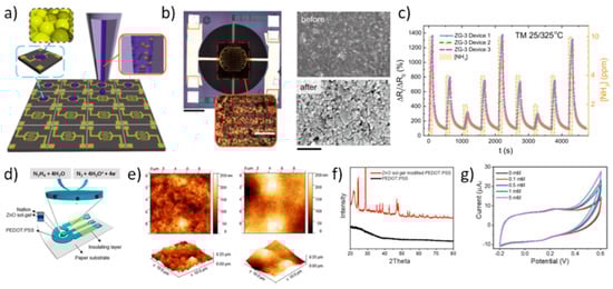
Figure 15.
Applications in chemosensors. (a) Schematic representation of the graphene-ZnO inkjet printing deposition process over multiple CMOS μHPs. (b) Optical micrograph of a single inkjet-printed device (scale bar 200 μm), and magnification of the graphene-ZnO NP film over the Au interdigitated electrodes (IDEs, scale bar 20 μm) (left panel); scanning electron microscope (SEM) image of the graphene-ZnO composite film before and after thermal annealing (right panel). (c) Device response curves by the temperature-modulation scheme upon nine pure NH3 injection cycles (10, 4, and 2 ppm) (3 wt% graphene sample, ZG-3). Reprinted from reference [124] under a Creative Commons Attribution 4.0 International License. (d) All inkjet-printed PEDOT:PSS/ZnO sensor for hydrazine detection, schematic structure. (e) AFM images of PEDOT:PSS/ZnO (left panel), and PEDOT:PSS (right panel) electrode surfaces. (f) X-ray diffraction (XRD) spectra of PEDOT:PSS/ZnO (red) and PEDOT:PSS (black line) electrodes. (g) CV response of the PEDOT:PSS/ZnO electrode sensor in the presence of different concentrations of hydrazine (0 mM to 5 mM). Reprinted from Reference [125], Copyright (2020), with permission from Elsevier.
As far as the fabrication of UV photodetectors based on printed ZnO ink formulations is concerned, in the last decade different approaches have been proposed to improve detector performance, as well as integration on flexible substrates. In particular, some intriguing studies reported on enhanced photoresponse of inkjetted ZnO thin films by embedding other NPs to improve interfacial charge transfer. Wu and coworkers [126] demonstrated that the photoconductivity of ZnO NP thin films fabricated by DOD inkjet printing (treated at 400 °C to achieve crystallization) and then capped with CdS NPs, was improved by three orders of magnitude under UV irradiation, with respect to the pure ZnO film (Figure 16a–d). The decay time was also reduced to ~4 ms. Capping with CdS, whose deposition followed inkjet printing of ZnO NPs, suppressed passivation of the ZnO film and improved interfacial charge transfer, thereby reducing carrier recombination. More recently, Cook et al. [127] enhanced interfacial charge transfer by leveraging a nanocomposite ink formed by graphene nanoplatelets (GnP) incorporated in a ZnO precursor (ZnOPr) solution to print UV photodetectors. A network of bulk heterojunctions of ZnO/ GnP was then formed during the ZnO crystallization process in the post-annealing after inkjet printing. An UV responsivity of 2.2 A/W (incident UV power of 2.2 μW, 5 V bias) was achieved at the optical GnP concentration of 20 mM. In a previous work, Cook et al. [128] also reported on a nanocomposite ink formulated with ZnOPr and crystalline ZnO QDs, which allowed for inkjet printing of high-performance photodetectors exhibiting UV responsivity of 383.6 A/W and on/off ratio of 2470. The embedded QDs promoted both nanoporous structure of the ZnO printed film with improved crystallinity, thereby reducing the growth of defects and impurities.
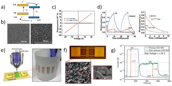
Figure 16.
Applications in ultraviolet (UV) photodetection. (a) Sketch of the energy diagram of the CdS/ZnO nanocomposite indicating interfacial charge-transfer. (b) Top-view SEM micrograph of the pure ZnO film (left panel) and of the CdS NP dip-coated film (right panel) (precursor of 0.0125 M concentration, 5 dip cycles). (c) Current-voltage characteristics of CdS/ZnO film (CdS precursor concentration of 0.0125 M, 5 dip cycles) under dark and UV irradiation conditions (black and red symbols, respectively). (d) Photoresponse vs. time under UV irradiation “on” and “off” conditions for the CdS capped ZnO device compared to pure ZnO film and CdS film (left panel; blue, red, and black symbols, respectively). Magnification of the decay process for the CdS/ZnO nanocomposite and ZnO films (right panel). Reprinted with permission from Reference [126]. Copyright 2010 American Chemical Society. (e) Schematic diagram of the aerosol jet deposition head as printing the device architecture on the PET substrate: the conductive Ag contacts, and the ZnO active layer (left panel). Optical image of the whole flexible substrate patterned with an array of printed thin film ZnO photodetector elements (right panel). (f) Microscopic image of the device and SEM image of the ZnO films at different magnifications. (g) Photocurrent vs. time under switched “on” and “off” 252 nm UV light irradiation from printed photodetectors with porous and non-porous ZnO film. Reprinted with permission from Reference [131]. Copyright 2018 American Chemical Society.
The mild conditions afforded by inkjet printing made it particularly suited for printing ZnO thin film as an active layer in flexible substrates for UV radiation detection and monitoring [129,130]. In these works all inkjet-printed flexible UV photodetector arrays were fabricated by patterning both conductive material for electrodes (typically, Ag) and the ZnO NP active layer on flexible plastic substrates, such as Kapton polyimide film [129] and polyethylene terephthalate (PET) [130]. Similar behavior upon UV irradiation was reported, with light on/off ratio >103 and good reproducibility over long-term repeated bending cycles. A different technological approach was proposed by Gupta et al. [131] who fabricated all printed high-performance nanoporous ZnO UV detectors by aerosol-jet printing. In this process, an aerosol gas stream containing the functional ink to be printed is focused to the surface by an inert sheath gas, thus reducing the sprayover. Both Ag contacts and ZnO nanocrystals were printed over a PET substrate forming the final detector array (Figure 16e). A relatively low temperature annealing procedure at 150 °C in N2 atmosphere followed the material deposition to remove residual solvent, which favourably made the developed methodology compatible with flexible, inexpensive substrates. As demonstrated by SEM analysis, the ZnO film morphology was a well-connected polycrystalline porous network with high surface to volume ratio (Figure 16f). The devices showed a light on/off ratio as high as 106 and short response times (Figure 15g).
ZnO NP inks have been leveraged for a number of applications in the field of inkjet printing of electronic and optoelectronic devices, which has experienced a tremendous growth in the last decades [132,133,134]. In particular, ink-jet printing has emerged as an attractive patterning approach for various organic electronic materials, conducting NP solutions, UV-curable adhesives, and even biomaterials such as DNA [132]. All-polymer thin-film transistor (TFT) circuits were successfully demonstrated overcoming limitations in resolution of inkjet printing due to statistical variations of the flight direction of droplets and their spreading on the substrate [135]. Thereafter, researchers reported on inkjet printing of contacts and interconnects based on metal- and metal oxide-containing inks for printed electronics [136,137]. Printed TFT devices based on inkjetted ZnO NPs have been reported in recent years. Liu et al. [138] followed a low-cost, mask-free approach to fabricate bottom-gate, top-contact TFTs where both the gate dielectric and the active channel were ink-jet printed by using ZnO NP and poly(4-viylphenol) (PVP) polymer matrix-based inks, respectively. However, this device exhibited relatively poor performance, with a current on/off ratio of 4 × 101, a carrier mobility of 0.69 cm2/Vs, and a threshold voltage of 25.5 V. Better results were achieved by Lim et al. [139] who also reported on a bottom-gate n-channel ZnO TFT, where a ZnO suspension of nanorods was inkjet-printed to pattern the ZnO active channel. They used a tetraethyl orthosilicate (TEOS) silicon oxide (SiO2) by plasma-enhanced CVD (300 nm thick) for the gate dielectric. A smooth and uniform ZnO thin film was fabricated with a resolution of 200 dpi and using droplets of 50 μm diameter and 35 pL volume (Figure 17a). Interestingly the authors report on the beneficial effect of annealing treatment (150 °C, 1 h) which improved both film crystallinity and electrical performance (Figure 17b,c). The former exhibited a marked predominance of the (002) diffraction peak (at around 34.4°), thereby indicating a wurtzite crystalline structure with a preferential orientation along the c-axis for the annealed film. As for the latter, the on/off current ratio, carrier mobility, and threshold voltage were 106, 3.03 cm2/Vs, and –3.3 V, respectively. Significantly higher performance was reported for TFTs using inkjet-printed ZnO based materials such as amorphous indium-gallium-zinc-oxide (a-IGZO) and amorphous indium zinc oxide (a-IZO). In particular, high mobility ink-jet printed IGZO TFTs with bottom-gate architecture and using a solution processed Sr-doped Al2O3 (SAO) gate dielectric were fabricated by Choi et al. [140], and exhibited on/off ratio and saturation field-effect mobility as high as 2.5 × 10⁶ and 30.7 cm2/Vs, respectively. Behera et al. [141] demonstrated high performance printed a-IZO FETs with field-effect mobility exceeding 27.5 cm2/Vs, well comparable to device mobility by inkjet printed a-IZO TFTs reported in previous works [142,143].
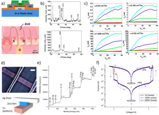
Figure 17.
Applications in electronic devices. (a) Bottom-gate architecture of an inkjet printed ZnO nanorod based thin-film transistor (TFT, upper panel), and optical micrograph of the device top-view. (b) XRD patterns of the inkjet printed ZnO film, RT-dried (upper panel) and after annealing at 150 °C for 1 h in oxygen. (c) Drain current – drain voltage characteristics of the ZnO nanorod based TFT dried for 10 and 60 min (upper panels, left and right, respectively), and annealed at 150 °C for 10 and 60 min (lower panels, left and right, respectively). Reproduced from Reference [139] Copyright (2014) The Japan Society of Applied Physics. (d) All inkjet printed ZnO NP based memristor device: optical microscopy image of one memristive pixel (upper panel, scale bar 100 μm), and schematic representation added to illustrate device elements (lower panel). (e) X-ray photoelectron spectroscopy (XPS) analysis of a printed ZnO NP film. (f) Semi-log plot of current-voltage sweeps (1st, 100th, and 500th sweeps) from one of the 9 memristor pixels. The bistable memristive behavior with the resistive switching to the low-resistance state (LRS) and to the high-resistance state (HRS) is indicated (sweep direction is indicated by arrows). Reproduced from Reference [145]. Copyright (2013), with permission from Elsevier.
Inkjet-printed ZnO has also been used to improve the performance of electronic devices as a support material. For instance, n-type organic TFTs are usually very difficult to achieve, and perform well below the p-type counterpart. This is mainly due to limited electronic injection between electrodes and organic semiconductor. Taking advantage of the superior features offered by inkjet printing, Roh et al. [144] demonstrated how the use of an inkjet-printed ZnO NP thin film as electron injection layer in an all-solution processed n-type organic field-effect transistor (OFET) could overcome these challenges; 2 wt% in density, ~1 cPs in viscosity ZnO NP ink was inkjet-printed onto Ag source and drain electrodes, followed by annealing at 100 °C in N2 atmosphere. The printed ZnO acted as an electrode-semiconductor interfacial layer, and the electrical performance of the engineered n-type OFET was dramatically improved with respect to the same device with spin-coated ZnO, and, even more, to that without the ZnO electron injection layer.
ZnO NP inks have also been leveraged by Muhammad et al. [145] for a novel, exciting application in all printed resistive-memory devices. By means of an electrohydrodynamic inkjet printing process at room temperature (RT) a 3 × 3 memristor array (i.e., a 9-bit memristor) was fabricated, based on a metal-insulator-metal structure made of printed Ag and Cu crossbars (top and bottom electrodes, respectively) and a ZnO nano-layer sandwiched between them (Figure 17d). A ZnO NP ink 10 wt.% in NP concentration and 6.25 cps in viscosity was prepared, electrosprayed through a 410 μm in inner diameter metallic nozzle over a 1 cm2 area over the bottom electrodes, and then sintered at 500 °C for 5h. The authors report a thorough characterization procedure based on XRD, X-ray photoelectron spectroscopy (XPS), and SEM techniques. In particular, the result of XPS analysis (Figure 17e) was that the ZnO active layer of the memristor device, printed at room conditions, had a good purity, except for some residuals (i.e., C peaks) from the acetate solution of the ink precursor. A composition of Zn:O:C = 28:64:8 was estimated. The current-voltage measurements clearly revealed the typical memristive hysteresis with a resistive switching phenomenon (Figure 17f), with an ON/OFF ratio relevant to the bipolar resistive switching of 1 × 10³, which was maintained with excellent reproducibility over the evaluated 500 sweeps.
Ink-jet printing of ZnO inks is also being intriguingly applied in photovoltaics, and in particular in the emerging field of organic solar cells (OSCs). Indeed, inkjet printing is increasingly recognized as a very promising technique for industrial-scale production of OSCs due the possibility of locally deposit small volumes of functional inks without a mask, low cost, simple and environmentally friendly fabrication process, and the reduction of material wasting. It has also proven effective in fabrication of all-inkjet-printed OSCs, which is an appealing perspective for both industry and research. Due to the good electron mobility and the transparency in the whole visible region, inkjet-printed ZnO has attracted a lot of interest as the ETL in conventional as well as in the higher performance inverted polymer solar cell (PSCs), mostly based on the widely preferred bulk-heterojunction (BHJ) structure with P3HT:PCBM blends as photoactive layer. For instance, Jung et al. [146] demonstrated for the first time all-inkjet-printed, all-air-processed OSCs with an average PCE of 2%, based on the structure glass substrate/PEDOT:PSS/ poly[N-9′- heptadecanyl-2,7-carbazole-alt-5,5-(4′,7′-di-2-thienyl-2′,1′,3′-benzothiadiazole)]:[6,6]-phenyl-C71-butyric acid methyl ester (PCDTBT:PC70BM)/ZnO/Ag (Figure 18a–c). The ZnO NP layer served as ETL, as well as to protect the photoactive layer from the solvent of the Ag NP ink. A single nozzle homebuilt inkjet printer with a piezoelectric MJ-A print head was used for OSC fabrication and the active area of the single device was about 0.5 cm2. Interestingly, two types of ZnO nanoparticle inks in methanol were synthetized, based on ZnO nanorods and ZnO quantum dots. Different PCEs of 2.05% and 0.76% were found for the all printed solar cells fabricated with ZnO QD and ZnO NR inks, respectively. Although referred to structures whose printing process was not-fully optimized, the surprisingly lower PCE exhibited by the ZnO NR-based OSC was reasonably ascribed to inefficient ordering of printed ZnO NRs in the ETL causing a higher trap density. ZnO NPs synthetized by hydrothermal condensation of Zn(acetate) were used by Eggenhuisen et al. [147] who reported on larger area (>1 cm2) fully inkjet printed solar cells produced by an environmental friendly approach avoiding the use of chlorinated solvent mixtures in the deposition of functional layers. OSCs with the structure high-conductive (HC) PEDOT/ZnO NPs/photoactive layer/PEDOT were fabricated using an industrial printhead and non-halogenated solvents only. Using P3HT:PC60BM as the photoactive layer, an average PCE of 1.7% was achieved, which increased up to 4.1% when a more expensive ActivInk PV2000 photoactive layer was employed. Further reports have demonstrated the use of inkjetted ZnO NPs in higher-performance inverted PSCs.
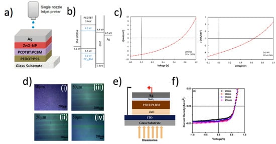
Figure 18.
Applications in photovoltaics. (a) Device architecture and (b) schematic energy level diagram of a Glass/PEDOT:PSS/PCDTBT:PC70BM/ZnO-NP/Ag all-inkjet-printed solar cell. (c) J-V characteristics under illumination of the organic solar cells (OSCs) based on ZnO ETL fabricated with ZnO quantum dots (left panel) and nanorods (right panel). The respective PCEs are indicated. Reproduced with permission from Reference [146]. Copyright © 2014 WILEY-VCH. (d) Optical micrographs of ZnO inkjet-printed films with 50 μm drop spacing using inks of viscosity (i) 2.07 cP, (ii) 2.43 cP, (iii) 2.90 cP, and (iv) 4.70 cP. (e) Architecture of the inverted OSC device structure, and (f) J-V characteristics under illumination of OSC devices with ink-jet printed P3HT:PC61BM blend active layer, and ZnO ETL of different thickness. Reproduced from Reference [148]. Copyright (2016), with permission from Elsevier.
A thorough investigation upon the mechanism of ink-jet printed ZnO film formation and the influence of printing parameters on the film growth was reported by Singh et al. [148]. They studied both the jetting behavior as a function of ink viscosity and the influence of surface treatment, ink concentration, drop spacing, substrate temperature during printing, and annealing temperature. Optimal parameters were a drop spacing of 40–50 μm and an ink viscosity of 4.70 cP, with the substrate held at room temperature. The formation of continuous ZnO thin films with controlled thickness was then demonstrated (Figure 18d). Investigations by AFM confirmed the nanocrystalline structure of the films with different roughness (0.8 ± 0.1 nm, ZnO annealed at 175 °C; 1.2 ± 0.1 nm, ZnO annealed at 250 °C). These results highlighted the fact that too high annealing temperature increased film roughness, thereby reducing light transmission and leading to higher trap density. Inverted PSCs based on printed ZnO films were fabricated with the structure Glass/ITO/ZnO/P3HT:PC61BM/MoO3/Ag (Figure 18e,f), which showed a maximum PCE of ~3.5% for spin coated photoactive blend film on printed ZnO, and 3.2% for the fully printed solar cell. In a further work, Sanchez et al. [149] reported on inverted PSCs with the architecture ITO/inkjet-printed ZnO/PTB7-Th:PC70BM/V2O5/Ag with PCE of 7.47%. The authors studied different recombination mechanisms in solar cells whose ZnO ETL was made by inkjet printing, spin coating, and thermal evaporation, showing how the different deposition approaches induce a variation of the band structure of the active layer deposited over the zinc oxide. In another report, Ganesan et al. [150] prepared by inkjet printing ZnO ETL and P3HT:ICBA photoactive blends in a Glass/ITO/ZnO/P3HT:ICBA/MoO3/Ag structure exhibiting a PCE of 4.7%.
8. ZnO-Based Nanolithography Printed Devices
ZnO inks have also been developed for printing by DPN. Herein, some examples of DPN patterning of ZnO inks are shown, for applications in fields like printed electronics and chemical sensing. The first step for ZnO deposition by DPN is the ink formulation. In fact, ZnO inks can be prepared through a sol-gel synthesis starting from a zinc salt precursor in an alkaline solution, e.g., zinc acetate dihydrate (Zn(CH3OO)2·2H2O) in isopropyl alcohol and monoethanolamine [151]. Glycerol is generally introduced as cosolvent in order to tune the physicochemical properties of the ink [152]. The resulting fluid can be deposited as liquid ink on virtually any kind of solid substrate. However, in most cases an annealing step is required after the ZnO deposition, a technical aspect which can lead to a limitation in terms of the possible materials to use as substrates. In particular, some polymeric supports, but also ceramic and metallic materials, can be thermos-sensitive, or result in being modified after curing. In order to overcome this limitation, a DPN-based protocol has been developed, which involves a first step of ZnO ink patterning by DPN on glass, a substrate stable even at high temperature. After annealing (500 °C) on glass, the ZnO pattern was physically transferred on a polyethylene naphthalate (PEN) support by applying a 75 kPa pressure and heating at 190 °C [151]. Alternatively, it is also possible to print by DPN colloidal suspensions of ZnO nanostructures. For instance, S. Santra et al. deposited ZnO nanorods on a silicon on insulator (SOI) CMOS micro electro mechanical system (MEMS) μHP substrate [153]. They demonstrated the feasibility to use this system as a cheap sensor for ethanol detection and quantification in gaseous phase (Figure 19). In particular, the measured resistance of the system is highly sensitive to the composition of the gas mixture at the interface. Then, it was possible to detect the presence of ethanol at very low concentration (25–1000 ppm). Noteworthy, this ZnO-based gas sensor showed that the resistance measurement in this kind of setup is importantly affected by the relative humidity, a fundamental aspect to take into account for real life application [153]. Other elongated ZnO nanostructures have also been used for the fabrication of interesting devices by DPN. In particular, an n-type FET has been developed exploiting the high spatial control in positioning ZnO pattern to a precision of a few nanometers [154]. Employing a ZnO precursor solution as liquid ink, fluid lines of ink have been deposited on a sapphire grid on which nanometric edges (1.3 nm) are present [153]. After annealing at 1200 °C aligned ZnO nanowires were obtained for application as transistor. The systems obtained by DPN are of tremendous technological relevance as the high accuracy and resolution in positioning nanostructures is a key point for technological advances and improvements in device performance.
Figure 19.
Applications in ethanol sensors. Ethanol sensor based on ZnO deposited by DPN. (a) Schematic diagram of the CMOS micro electro mechanical system (MEMS) micro-hotplate cross section, where the different components and their relative positions are depicted; (b) optical micrograph of the fabricated ethanol sensor (dimensions 1 mm × 1 mm). (c) Sensor response to the presence of gaseous ethanol in the range of 0–1000 ppm is also reported, showing the high sensitivity of the ZnO printed device. Republished with permission from the Royal Society of Chemistry, from Reference [153]; permission conveyed through Copyright Clearance Center, Inc.
9. Conclusions
Printing processes offer unique large-area processing capability and high throughput fabrication for the integration of (nano)crystalline materials in functional devices under mild operative, low-cost, and often environmentally friendly conditions, permitting to reduce materials wastage. This review intends to provide an unprecedented view on ZnO-based ink printing, highlighting the different ink formulations and the most relevant printing approaches so far explored in the literature (namely, screen printing, flexographic printing, 3D printing, inkjet printing, and dip pen nanolithography). In the current scenario, the researchers often have to carefully formulate the “printing inks” by tuning the most relevant physicochemical properties (e.g., viscosity, precursor concentration, surface tension, printing speed) in order to fit the requirements of each methodology. Typically, this results in preparing ZnO-based inks (based on the stable dispersion of ZnO nanomaterials) that are stable enough during the printing process, leading to the formation of continuous, ordered and often crystalline films of thickness ranging from nano- to micro-scale. Many reports also show, as an alternative, the possibility to print solution-based precursors (containing a soluble zinc salt and an additive) leading to the formation of ZnO nano- to microstructures onto solid surfaces after heating. This approach has the advantage of using soluble precursors that do not lead to aggregation issues of the ZnO nanomaterials in the ink. In the review, we have offered a rapid overview of the most relevant applications based on printable ZnO-based inks. The extraordinary versatility and the large number of properties of ZnO result in a very broad range of applications of the resulting printed devices, including chemical and physical sensors, photocatalysis, solar cells, thin film transistors, memristors and other ones. Among the methods herein explored, inkjet printing seems to provide the highest number of applications, likely due to the higher number of printable formulations, its lower cost, excellent lateral resolution, and low material consumption. This study does not intend to offer the reader all the literature currently available, however, we hope to have reviewed the most relevant aspects of this emerging-research field, with the ultimate goal to highlight the importance of printing technologies in the sustainable fabrication of ZnO-based devices.
Author Contributions
Methodology, G.A., Y.A., V.F., R.P.; writing—original draft preparation, G.A., G.P.; writing—review and editing, G.A. and G.P.; supervision, G.A., G.P., B.P. and P.G.M. All authors have read and agreed to the published version of the manuscript.
Funding
The work was financially supported by the University of Palermo and by the project Tyre Recycling for Clean Seas (Ty.Re.C.S), CUP:E86C18002290002.
Acknowledgments
We acknowledge the Advanced Technologies Network (ATeN) Center, Università degli Studi di Palermo, Ed. 18, V.le delle Scienze, 90128 Palermo, Italy, for hospitality and support and Mauro Tomassetti for fruitful discussion.
Conflicts of Interest
The authors declare no conflict of interest.
References
- Marques, G.C.; Rasheed, F.; Aghassi-Hagmann, J.; Tahoori, M.B. From silicon to printed electronics: A coherent modeling and design flow approach based on printed electrolyte gated FETs. In Proceedings of the 2018 23rd Asia and South Pacific Design Automation Conference (ASP-DAC), Jeju, Korea, 22–25 January 2018; IEEE: Jeju, Korea, 2018; pp. 658–663. [Google Scholar]
- Michel, B.; Bernard, A.; Bietsch, A.; Delamarche, E.; Geissler, M.; Juncker, D.; Kind, H.; Renault, J.P.; Rothuizen, H.; Schmid, H.; et al. Printing meets lithography: Soft approaches to high-resolution patterning. IBM J. Res. Dev. 2001, 45, 697–719. [Google Scholar] [CrossRef]
- Aleeva, Y.; Pignataro, B. Recent advances in upscalable wet methods and ink formulation for printed electronics. J. Mater. Chem. C 2014, 2, 6436–6453. [Google Scholar] [CrossRef]
- Arrabito, G.; Pignataro, B. Solution Processed Micro- and Nano-Bioarrays for Multiplexed Biosensing. Anal. Chem. 2012, 84, 5450–5462. [Google Scholar] [CrossRef] [PubMed]
- Kim, J.; Kumar, R.; Bandodkar, A.J.; Wang, J. Advanced Materials for Printed Wearable Electrochemical Devices: A Review. Adv. Electron. Mater. 2017, 3, 1600260. [Google Scholar] [CrossRef]
- Arrabito, G.; Pignataro, B. Inkjet Printing Methodologies for Drug Screening. Anal. Chem. 2010, 82, 3104–3107. [Google Scholar] [CrossRef]
- Arrabito, G.; Cavaleri, F.; Montalbano, V.; Vetri, V.; Leone, M.; Pignataro, B. Monitoring few molecular binding events in scalable confined aqueous compartments by raster image correlation spectroscopy (CADRICS). Lab Chip 2016, 16, 4666–4676. [Google Scholar] [CrossRef]
- Arrabito, G.; Errico, V.; De Ninno, A.; Cavaleri, F.; Ferrara, V.; Pignataro, B.; Caselli, F. Oil-in-Water fL Droplets by Interfacial Spontaneous Fragmentation and Their Electrical Characterization. Langmuir 2019, 35, 4936–4945. [Google Scholar] [CrossRef]
- Gandor, S.; Reisewitz, S.; Venkatachalapathy, M.; Arrabito, G.; Reibner, M.; Schröder, H.; Ruf, K.; Niemeyer, C.M.; Bastiaens, P.I.H.; Dehmelt, L. A Protein-Interaction Array Inside a Living Cell. Angew. Chem. Int. Ed. 2013, 52, 4790–4794. [Google Scholar] [CrossRef] [PubMed]
- Arrabito, G.; Schroeder, H.; Schröder, K.; Filips, C.; Marggraf, U.; Dopp, C.; Venkatachalapathy, M.; Dehmelt, L.; Bastiaens, P.I.H.; Neyer, A.; et al. Configurable Low-Cost Plotter Device for Fabrication of Multi-Color Sub-Cellular Scale Microarrays. Small 2014, 10, 2870–2876. [Google Scholar] [CrossRef]
- Anderson, D.M. Imbibition of a liquid droplet on a deformable porous substrate. Phys. Fluids 2005, 17, 87104. [Google Scholar] [CrossRef]
- Zhang, F.; Wei, M.; Viswanathan, V.V.; Swart, B.; Shao, Y.; Wu, G.; Zhou, C. 3D printing technologies for electrochemical energy storage. Nano Energy 2017, 40, 418–431. [Google Scholar] [CrossRef]
- Huang, Q.; Zhu, Y. Printing Conductive Nanomaterials for Flexible and Stretchable Electronics: A Review of Materials, Processes, and Applications. Adv. Mater. Technol. 2019, 4, 1800546. [Google Scholar] [CrossRef]
- Matsui, H.; Takeda, Y.; Tokito, S. Flexible and printed organic transistors: From materials to integrated circuits. Org. Electron. 2019, 75, 105432. [Google Scholar] [CrossRef]
- Minemawari, H.; Yamada, T.; Matsui, H.; Tsutsumi, J.; Haas, S.; Chiba, R.; Kumai, R.; Hasegawa, T. Inkjet printing of single-crystal films. Nature 2011, 475, 364–367. [Google Scholar] [CrossRef] [PubMed]
- Kang, B.J.; Oh, J.H. Control of the crystalline structure of inkjet-printed semiconductor layers using overlap condition and surface wettability. J. Micromech. Microeng. 2015, 25, 055011. [Google Scholar] [CrossRef]
- Rödlmeier, T.; Marszalek, T.; Held, M.; Beck, S.; Müller, C.; Eckstein, R.; Morfa, A.J.; Lovrincic, R.; Pucci, A.; Lemmer, U.; et al. Controlled Molecular Orientation of Inkjet Printed Semiconducting Polymer Fibers by Crystallization Templating. Chem. Mater. 2017, 29, 10150–10158. [Google Scholar] [CrossRef]
- Khan, Y.; Thielens, A.; Muin, S.; Ting, J.; Baumbauer, C.; Arias, A.C. A New Frontier of Printed Electronics: Flexible Hybrid Electronics. Adv. Mater. 2019, 1905279. [Google Scholar] [CrossRef]
- Wu, W. Inorganic nanomaterials for printed electronics: A review. Nanoscale 2017, 9, 7342–7372. [Google Scholar] [CrossRef]
- Tseng, Y.-K.; Chuang, M.-H.; Chen, Y.-C.; Wu, C.-H. Synthesis of 1D, 2D, and 3D ZnO Polycrystalline Nanostructures Using the Sol-Gel Method. J. Nanotechnol. 2012, 2012, 1–8. [Google Scholar] [CrossRef]
- Ravirajan, P.; Peiró, A.M.; Nazeeruddin, M.K.; Graetzel, M.; Bradley, D.D.C.; Durrant, J.R.; Nelson, J. Hybrid Polymer/Zinc Oxide Photovoltaic Devices with Vertically Oriented ZnO Nanorods and an Amphiphilic Molecular Interface Layer. J. Phys. Chem. B 2006, 110, 7635–7639. [Google Scholar] [CrossRef]
- Errico, V.; Arrabito, G.; Plant, S.R.; Medaglia, P.G.; Palmer, R.E.; Falconi, C. Chromium inhibition and size-selected Au nanocluster catalysis for the solution growth of low-density ZnO nanowires. Sci. Rep. 2015, 5, 12336. [Google Scholar] [CrossRef]
- Garces, H.F.; Espinal, A.E.; Suib, S.L. Tunable Shape Microwave Synthesis of Zinc Oxide Nanospheres and Their Desulfurization Performance Compared with Nanorods and Platelet-Like Morphologies for the Removal of Hydrogen Sulfide. J. Phys. Chem. C 2012, 116, 8465–8474. [Google Scholar] [CrossRef]
- Lei, Y.; Luo, N.; Yan, X.; Zhao, Y.; Zhang, G.; Zhang, Y. A highly sensitive electrochemical biosensor based on zinc oxide nanotetrapods for l-lactic acid detection. Nanoscale 2012, 4, 3438–3443. [Google Scholar] [CrossRef]
- Vabbina, P.K.; Kaushik, A.; Pokhrel, N.; Bhansali, S.; Pala, N. Electrochemical cortisol immunosensors based on sonochemically synthesized zinc oxide 1D nanorods and 2D nanoflakes. Biosens. Bioelectron. 2015, 63, 124–130. [Google Scholar] [CrossRef]
- Chaudhary, S.; Umar, A.; Bhasin, K.; Baskoutas, S. Chemical Sensing Applications of ZnO Nanomaterials. Materials 2018, 11, 287. [Google Scholar] [CrossRef] [PubMed]
- Pandurangan, M.; Kim, D.H. In vitro toxicity of zinc oxide nanoparticles: A review. J. Nanopart Res. 2015, 17, 158. [Google Scholar] [CrossRef]
- Massaro, M.; Casiello, M.; D’Accolti, L.; Lazzara, G.; Nacci, A.; Nicotra, G.; Noto, R.; Pettignano, A.; Spinella, C.; Riela, S. One-pot synthesis of ZnO nanoparticles supported on halloysite nanotubes for catalytic applications. Appl. Clay Sci. 2020, 189, 105527. [Google Scholar] [CrossRef]
- Falconi, C. Piezoelectric nanotransducers. Nano Energy 2019, 59, 730–744. [Google Scholar] [CrossRef]
- Wang, Z.L.; Song, J. Piezoelectric Nanogenerators Based on Zinc Oxide Nanowire Arrays. Science 2006, 312, 242. [Google Scholar] [CrossRef]
- Nour, E.S.; Bondarevs, A.; Huss, P.; Sandberg, M.; Gong, S.; Willander, M.; Nur, O. Low-Frequency Self-Powered Footstep Sensor Based on ZnO Nanowires on Paper Substrate. Nanoscale Res. Lett. 2016, 11, 156. [Google Scholar] [CrossRef]
- Asif, M.H.; Ali, S.M.U.; Nur, O.; Willander, M.; Brännmark, C.; Strålfors, P.; Englund, U.H.; Elinder, F.; Danielsson, B. Functionalised ZnO-nanorod-based selective electrochemical sensor for intracellular glucose. Biosens. Bioelectron. 2010, 25, 2205–2211. [Google Scholar] [CrossRef] [PubMed]
- Bhat, S.S.; Qurashi, A.; Khanday, F.A. ZnO nanostructures based biosensors for cancer and infectious disease applications: Perspectives, prospects and promises. TRAC Trends Anal. Chem. 2017, 86, 1–13. [Google Scholar] [CrossRef]
- Zhu, G.; Wang, A.C.; Liu, Y.; Zhou, Y.; Wang, Z.L. Functional Electrical Stimulation by Nanogenerator with 58 V Output Voltage. Nano Lett. 2012, 12, 3086–3090. [Google Scholar] [CrossRef] [PubMed]
- Asif, M.; Danielsson, B.; Willander, M. ZnO Nanostructure-Based Intracellular Sensor. Sensors 2015, 15, 11787–11804. [Google Scholar] [CrossRef]
- Xu, C.; Wu, J.; Desai, U.V.; Gao, D. Multilayer Assembly of Nanowire Arrays for Dye-Sensitized Solar Cells. J. Am. Chem. Soc. 2011, 133, 8122–8125. [Google Scholar] [CrossRef]
- Rong, P.; Ren, S.; Yu, Q. Fabrications and Applications of ZnO Nanomaterials in Flexible Functional Devices-A Review. Crit. Rev. Anal. Chem. 2019, 49, 336–349. [Google Scholar] [CrossRef]
- Krebs, F.C. Fabrication and processing of polymer solar cells: A review of printing and coating techniques. Sol. Energy Mater. Sol. Cells 2009, 93, 394–412. [Google Scholar] [CrossRef]
- Kapur, N.; Abbott, S.J.; Dolden, E.D.; Gaskell, P.H. Predicting the Behavior of Screen Printing. IEEE Trans. Compon. Packag. Manufact. Technol. 2013, 3, 508–515. [Google Scholar] [CrossRef]
- Wen, Y.; Liu, Y.; Guo, Y.; Yu, G.; Hu, W. Experimental Techniques for the Fabrication and Characterization of Organic Thin Films for Field-Effect Transistors. Chem. Rev. 2011, 111, 3358–3406. [Google Scholar] [CrossRef]
- Seigo, I. (Ed.) Abdullah Uzum Non-Vacuum Process for Production of Crystalline Silicon Solar Cells. In New Research on Silicon; IntechOpen: Rijeka, Croatia, 2017; Chapter 5. [Google Scholar]
- Scheideler, W.J.; Smith, J.; Deckman, I.; Chung, S.; Arias, A.C.; Subramanian, V. A robust, gravure-printed, silver nanowire/metal oxide hybrid electrode for high-throughput patterned transparent conductors. J. Mater. Chem. C 2016, 4, 3248–3255. [Google Scholar] [CrossRef]
- Noh, J.; Yeom, D.; Lim, C.; Cha, H.; Han, J.; Kim, J.; Park, Y.; Subramanian, V.; Cho, G. Scalability of Roll-to-Roll Gravure-Printed Electrodes on Plastic Foils. IEEE Trans. Electron. Packag. Manufact. 2010, 33, 275–283. [Google Scholar] [CrossRef]
- Kang, H.; Kitsomboonloha, R.; Jang, J.; Subramanian, V. High-Performance Printed Transistors Realized Using Femtoliter Gravure-Printed Sub-10 μm Metallic Nanoparticle Patterns and Highly Uniform Polymer Dielectric and Semiconductor Layers. Adv. Mater. 2012, 24, 3065–3069. [Google Scholar] [CrossRef] [PubMed]
- Yang, J.; Vak, D.; Clark, N.; Subbiah, J.; Wong, W.W.H.; Jones, D.J.; Watkins, S.E.; Wilson, G. Organic photovoltaic modules fabricated by an industrial gravure printing proofer. Sol. Energy Mater. Sol. Cells 2013, 109, 47–55. [Google Scholar] [CrossRef]
- Kitsomboonloha, R.; Morris, S.J.S.; Rong, X.; Subramanian, V. Femtoliter-Scale Patterning by High-Speed, Highly Scaled Inverse Gravure Printing. Langmuir 2012, 28, 16711–16723. [Google Scholar] [CrossRef]
- Huang, Q.; Zhu, Y. Gravure Printing of Water-based Silver Nanowire ink on Plastic Substrate for Flexible Electronics. Sci. Rep. 2018, 8, 15167. [Google Scholar] [CrossRef] [PubMed]
- Liu, X.; Guthrie, J.T. A review of flexographic printing plate development. Surf. Coat. Int. Part B Coat. Trans. 2003, 86, 91–99. [Google Scholar] [CrossRef]
- Mogg, B.T.; Claypole, T.; Deganello, D.; Phillips, C. Flexographic printing of ultra-thin semiconductor polymer layers. Transl. Mater. Res. 2016, 3, 015001. [Google Scholar] [CrossRef]
- Brumm, P.; Sauer, H.; Dörsam, E. Scaling Behavior of Pattern Formation in the Flexographic Ink Splitting Process. Colloids Interfaces 2019, 3, 37. [Google Scholar] [CrossRef]
- Morgan, M.L.; Holder, A.; Curtis, D.J.; Deganello, D. Formulation, characterisation and flexographic printing of novel Boger fluids to assess the effects of ink elasticity on print uniformity. Rheol. Acta 2018, 57, 105–112. [Google Scholar] [CrossRef]
- Kim, S.; Sojoudi, H.; Zhao, H.; Mariappan, D.; McKinley, G.H.; Gleason, K.K.; Hart, A.J. Ultrathin high-resolution flexographic printing using nanoporous stamps. Sci. Adv. 2016, 2, e1601660. [Google Scholar] [CrossRef]
- Campbell, T.A.; Ivanova, O.S. 3D printing of multifunctional nanocomposites. Nano Today 2013, 8, 119–120. [Google Scholar] [CrossRef]
- Chen, Z.; Li, Z.; Li, J.; Liu, C.; Lao, C.; Fu, Y.; Liu, C.; Li, Y.; Wang, P.; He, Y. 3D printing of ceramics: A review. J. Eur. Ceram. Soc. 2019, 39, 661–687. [Google Scholar] [CrossRef]
- Mazzanti, V.; Malagutti, L.; Mollica, F. FDM 3D Printing of Polymers Containing Natural Fillers: A Review of their Mechanical Properties. Polymers 2019, 11, 1094. [Google Scholar] [CrossRef]
- Derby, B. Bioprinting: Inkjet printing proteins and hybrid cell-containing materials and structures. J. Mater. Chem. 2008, 18, 5717–5721. [Google Scholar] [CrossRef]
- Li, J.; Macdonald, J. Lab on a Chip Inkjet printing for biosensor fabrication: Combining chemistry and technology for Inkjet printers. Lab Chip 2015, 15, 2538–2558. [Google Scholar] [CrossRef]
- Miccichè, C.; Arrabito, G.; Amato, F.; Buscarino, G.; Agnello, S.; Pignataro, B. Inkjet printing Ag nanoparticles for SERS hot spots. Anal. Methods 2018, 10, 3215–3223. [Google Scholar] [CrossRef]
- Ferrara, V.; Zito, G.; Arrabito, G.; Cataldo, S.; Scopelliti, M.; Giordano, C.; Vetri, V.; Pignataro, B. Aqueous Processed Biopolymer Interfaces for Single-Cell Microarrays. ACS Biomater. Sci. Eng. 2020. [Google Scholar] [CrossRef]
- Arrabito, G.; Galati, C.; Castellano, S.; Pignataro, B. Luminometric sub-nanoliter droplet-to-droplet array (LUMDA) and its application to drug screening by phase I metabolism enzymes. Lab Chip 2013, 13, 68–72. [Google Scholar] [CrossRef]
- Arrabito, G.; Cavaleri, F.; Porchetta, A.; Ricci, F.; Vetri, V.; Leone, M.; Pignataro, B. Printing Life-Inspired Subcellular Scale Compartments with Autonomous Molecularly Crowded Confinement. Adv. Biosyst. 2019, 3, 1900023. [Google Scholar] [CrossRef]
- Sanjana, N.E.; Fuller, S.B. A fast flexible ink-jet printing method for patterning dissociated neurons in culture. J. Neurosci. Methods 2004, 136, 151–163. [Google Scholar] [CrossRef] [PubMed]
- Zhang, Y.; Li, D.; Liu, Y.; Wittstock, G. Printing with Satellite Droplets. Small 2018, 14, 1802583. [Google Scholar] [CrossRef] [PubMed]
- Huang, T.-T.; Wu, W. Scalable nanomanufacturing of inkjet-printed wearable energy storage devices. J. Mater. Chem. A 2019, 7, 23280–23300. [Google Scholar] [CrossRef]
- Piner, R.D.; Zhu, J.; Xu, F.; Hong, S.; Mirkin, C.A. “Dip-Pen” Nanolithography. Science 1999, 283, 661–663. [Google Scholar] [CrossRef] [PubMed]
- Arrabito, G.; Reisewitz, S.; Dehmelt, L.; Bastiaens, P.I.; Pignataro, B.; Schroeder, H.; Niemeyer, C.M. Biochips for Cell Biology by Combined Dip-Pen Nanolithography and DNA-Directed Protein Immobilization. Small 2013, 9, 4243–4249. [Google Scholar] [CrossRef] [PubMed]
- Urtizberea, A.; Hirtz, M.; Fuchs, H. Ink transport modelling in Dip-Pen Nanolithography and Polymer Pen Lithography. Nanofabrication 2016, 2. [Google Scholar] [CrossRef]
- Liu, G.; Hirtz, M.; Fuchs, H.; Zheng, Z. Development of Dip-Pen Nanolithography (DPN) and Its Derivatives. Small 2019, 15, 1900564. [Google Scholar] [CrossRef]
- Brown, K.A.; Eichelsdoerfer, D.J.; Liao, X.; He, S.; Mirkin, C.A. Material transport in dip-pen nanolithography. Front. Phys. 2014, 9, 385–397. [Google Scholar] [CrossRef]
- Weeks, B.L.; Vaughn, M.W.; DeYoreo, J.J. Direct Imaging of Meniscus Formation in Atomic Force Microscopy Using Environmental Scanning Electron Microscopy. Langmuir 2005, 21, 8096–8098. [Google Scholar] [CrossRef]
- Hirtz, M.; Feng, W.; Fuchs, H.; Levkin, P.A. Click-Chemistry Immobilized 3D-Infused Microarrays in Nanoporous Polymer Substrates. Adv. Mater. Interfaces 2016, 3, 1500469. [Google Scholar] [CrossRef]
- Arrabito, G.; Ferrara, V.; Ottaviani, A.; Cavaleri, F.; Cubisino, S.; Cancemi, P.; Ho, Y.P.; Knudsen, B.R.; Hede, M.S.; Pellerito, C.; et al. Imbibition of Femtoliter-Scale DNA-Rich Aqueous Droplets into Porous Nylon Substrates by Molecular Printing. Langmuir 2019, 35, 17156–17165. [Google Scholar] [CrossRef]
- Huo, F.; Zheng, Z.; Zheng, G.; Giam, L.R.; Zhang, H.; Mirkin, C.A. Polymer Pen Lithography. Science 2008, 321, 1658–1660. [Google Scholar] [CrossRef] [PubMed]
- Kumar, R.; Urtizberea, A.; Ghosh, S.; Bog, U.; Rainer, Q.; Lenhert, S.; Fuchs, H.; Hirtz, M. Polymer Pen Lithography with Lipids for Large-Area Gradient Patterns. Langmuir 2017, 33, 8739–8748. [Google Scholar] [CrossRef] [PubMed]
- Naveed Ul Haq, A.; Nadhman, A.; Ullah, I.; Mustafa, G.; Yasinzai, M.; Khan, I. Synthesis Approaches of Zinc Oxide Nanoparticles: The Dilemma of Ecotoxicity. J. Nanomater. 2017, 2017, 1–14. [Google Scholar] [CrossRef]
- Fragalà, M.E.; Aleeva, Y.; Malandrino, G. ZnO nanorod arrays fabrication via chemical bath deposition: Ligand concentration effect study. Superlattices Microstruct. 2010, 48, 408–415. [Google Scholar] [CrossRef]
- Fragalà, M.E.; Aleeva, Y.; Malandrino, G. Effects of Metal-Organic Chemical Vapour Deposition grown seed layer on the fabrication of well aligned ZnO nanorods by Chemical Bath Deposition. Thin Solid Film 2011, 519, 7694–7701. [Google Scholar] [CrossRef][Green Version]
- Basinova, N.; Cernohorsky, O.; Grym, J.; Kucerova, S.; Faitova, H.; Yatskiv, R.; Vanis, J.; Vesely, J.; Maixner, J. Highly Textured Seed Layers for the Growth of Vertically Oriented ZnO Nanorods. Crystals 2019, 9, 566. [Google Scholar] [CrossRef]
- Zainelabdin, A.; Zaman, S.; Amin, G.; Nur, O.; Willander, M. Deposition of Well-Aligned ZnO Nanorods at 50 °C on Metal, Semiconducting Polymer, and Copper Oxides Substrates and Their Structural and Optical Properties. Cryst. Growth Des. 2010, 10, 3250–3256. [Google Scholar] [CrossRef]
- Prestopino, G.; Arrabito, G.; Generosi, A.; Mattoccia, A.; Paci, B.; Perez, G.; Verona-Rinati, G.; Medaglia, P.G. Emerging switchable ultraviolet photoluminescence in dehydrated Zn/Al layered double hydroxide nanoplatelets. Sci. Rep. 2019, 9, 11498. [Google Scholar] [CrossRef]
- Arrabito, G.; Falconi, C.; Errico, V.; Han, W. Zinc Oxide Nanowires on Printed Circuit Boards. In Proceedings of the Sensors; Compagnone, D., Baldini, F., Di Natale, C., Betta, G., Siciliano, P., Eds.; Springer International Publishing: Cham, Switzerland, 2015; pp. 271–275. [Google Scholar]
- Arrabito, G.; Errico, V.; Zhang, Z.; Han, W.; Falconi, C. Nanotransducers on printed circuit boards by rational design of high-density, long, thin and untapered ZnO nanowires. Nano Energy 2018, 46, 54–62. [Google Scholar] [CrossRef]
- Errico, V.; Arrabito, G.; Fornetti, E.; Fuoco, C.; Testa, S.; Saggio, G.; Rufini, S.; Cannata, S.; Desideri, A.; Falconi, C.; et al. High-Density ZnO Nanowires as a Reversible Myogenic–Differentiation Switch. ACS Appl. Mater. Interfaces 2018, 10, 14097–14107. [Google Scholar] [CrossRef]
- Lee, A.; Sudau, K.; Ahn, K.H.; Lee, S.J.; Willenbacher, N. Optimization of Experimental Parameters to Suppress Nozzle Clogging in Inkjet Printing. Ind. Eng. Chem. Res. 2012, 51, 13195–13204. [Google Scholar] [CrossRef]
- Lloyd, J.S.; Fung, C.M.; Deganello, D.; Wang, R.J.; Maffeis, T.G.G.; Lau, S.P.; Teng, K.S. Flexographic printing-assisted fabrication of ZnO nanowire devices. Nanotechnology 2013, 24, 195602. [Google Scholar] [CrossRef]
- Kwon, J.; Hong, S.; Lee, H.; Yeo, J.; Lee, S.S.; Ko, S. Direct selective growth of ZnO nanowire arrays from inkjet-printed zinc acetate precursor on a heated substrate. Nanoscale Res. Lett. 2013, 8, 489. [Google Scholar] [CrossRef] [PubMed]
- Güell, F.; Martínez-Alanis, P.R.; Khachadorian, S.; Zamani, R.R.; Franke, A.; Hoffmann, A.; Wagner, M.R.; Santana, G. Spatially controlled growth of highly crystalline ZnO nanowires by an inkjet-printing catalyst-free method. Mater. Res. Express 2016, 3, 025010. [Google Scholar] [CrossRef][Green Version]
- Zhang, B.; He, J.; Li, J.; Wang, L.; Li, D. Microscale electrohydrodynamic printing of in situ reactive features for patterned ZnO nanorods. Nanotechnology 2019, 30, 475301. [Google Scholar] [CrossRef] [PubMed]
- Greene, L.E.; Law, M.; Tan, D.H.; Montano, M.; Goldberger, J.; Somorjai, G.; Yang, P. General Route to Vertical ZnO Nanowire Arrays Using Textured ZnO Seeds. Nano Lett. 2005, 5, 1231–1236. [Google Scholar] [CrossRef]
- Plakhova, T.V.; Shestakov, M.V.; Baranov, A.N. Effect of textured seeds on the morphology and optical properties of solution- and vapor-grown ZnO nanorod arrays. Inorg. Mater. 2012, 48, 469–475. [Google Scholar] [CrossRef]
- Kitsomboonloha, R.; Baruah, S.; Myint, M.T.Z.; Subramanian, V.; Dutta, J. Selective growth of zinc oxide nanorods on inkjet printed seed patterns. J. Cryst. Growth 2009, 311, 2352–2358. [Google Scholar] [CrossRef]
- Ismail, B.; Abaab, M.; Rezig, B. Structural and electrical properties of ZnO films prepared by screen printing technique. Thin Solid Film 2001, 383, 92–94. [Google Scholar] [CrossRef]
- Suchat, S.; Potisart, J.; Supprakob, S.; Gitgeatpong, G.; Prachopchok, P. Comparison of ZnO film prepared by spray pyrolysis and screen printing methods. J. Metals Mater. Miner. 2019, 29, 58–69. [Google Scholar]
- Zargar, R.A.; Chackrabarti, S.; Joseph, S.; Khan, M.S.; Husain, R.; Hafiz, A.K. Synthesis and characterization of screen printed ZnO films for solar cell applications. Optik 2015, 126, 4171–4174. [Google Scholar] [CrossRef]
- Sarkar, K.; Rawolle, M.; Herzig, E.M.; Wang, W.; Buffet, A.; Roth, S.V.; Müller-Buschbaum, P. Custom-Made Morphologies of ZnO Nanostructured Films Templated by a Poly(styrene-block-ethylene oxide) Diblock Copolymer Obtained by a Sol-Gel Technique. ChemSusChem 2013, 6, 1414–1424. [Google Scholar] [CrossRef]
- Sarkar, K.; Braden, E.V.; Bonke, S.A.; Bach, U.; Müller-Buschbaum, P. Screen-Printing of ZnO Nanostructures from Sol–Gel Solutions for Their Application in Dye-Sensitized Solar Cells. ChemSusChem 2015, 8, 2696–2704. [Google Scholar] [CrossRef]
- de la Rubia López, M.A.; Peiteado, M.; Fernández, J.F.; Caballero, A.C.; Holc, J.; Drnovsek, S.; Kuscer, D.; Macek, S.; Kosec, M. Thick film ZnO based varistors prepared by screen printing. J. Eur. Ceram. Soc. 2006, 26, 2985–2989. [Google Scholar] [CrossRef]
- Carvalho, J.; Dubceac, V.; Grey, P.; Cunha, I.; Fortunato, E.; Martins, R.; Clausner, A.; Zschech, E.; Pereira, L. Fully Printed Zinc Oxide Electrolyte-Gated Transistors on Paper. Nanomaterials 2019, 9, 169. [Google Scholar] [CrossRef] [PubMed]
- Rai, P.; Kim, Y.-S.; Song, H.-M.; Song, M.-K.; Yu, Y.-T. The role of gold catalyst on the sensing behavior of ZnO nanorods for CO and NO2 gases. Sens. Actuators B Chem. 2012, 165, 133–142. [Google Scholar] [CrossRef]
- Candidato, R.T.; Ontolan, J.P.; Carpio, P.; Pawłowski, L.; Vequizo, R.M. Effects of precursor composition used in solution precursor plasma spray on the properties of ZnO coatings for CO2 and UV light sensing. Surf. Coat. Technol. 2019, 371, 395–400. [Google Scholar] [CrossRef]
- Manjunath, G.; Pujari, S.; Patil, D.R.; Mandal, S. A scalable screen-printed high performance ZnO-UV and Gas Sensor: Effect of solution combustion. Mater. Sci. Semicond. Process. 2020, 107, 104828. [Google Scholar] [CrossRef]
- Figueira, J.; Gaspar, C.; Carvalho, J.T.; Loureiro, J.; Fortunato, E.; Martins, R.; Pereira, L. Sustainable Fully Printed UV Sensors on Cork Using Zinc Oxide/Ethylcellulose Inks. Micromachines 2019, 10, 601. [Google Scholar] [CrossRef]
- Vilkman, M.; Apilo, P.; Välimäki, M.; Ylikunnari, M.; Bernardi, A.; Po, R.; Corso, G.; Hast, J. Gravure-Printed ZnO in Fully Roll-to-Roll Printed Inverted Organic Solar Cells: Optimization of Adhesion and Performance. Energy Technol. 2015, 3, 407–413. [Google Scholar] [CrossRef]
- Zhang, C.; Luo, Q.; Wu, H.; Li, H.; Lai, J.; Ji, G.; Yan, L.; Wang, X.; Zhang, D.; Lin, J.; et al. Roll-to-roll micro-gravure printed large-area zinc oxide thin film as the electron transport layer for solution-processed polymer solar cells. Org. Electron. 2017, 45, 190–197. [Google Scholar] [CrossRef]
- Assaifan, A.K.; Lloyd, J.S.; Samavat, S.; Deganello, D.; Stanton, R.J.; Teng, K.S. Nanotextured Surface on Flexographic Printed ZnO Thin Films for Low-Cost Non-Faradaic Biosensors. ACS Appl. Mater. Interfaces 2016, 8, 33802–33810. [Google Scholar] [CrossRef] [PubMed]
- Tubío, C.R.; Guitián, F.; Gil, A. Fabrication of ZnO periodic structures by 3D printing. J. Eur. Ceram. Soc. 2016, 36, 3409–3415. [Google Scholar] [CrossRef]
- Son, S.; Jung, P.-H.; Park, J.; Chae, D.; Huh, D.; Byun, M.; Ju, S.; Lee, H. Customizable 3D-printed architecture with ZnO-based hierarchical structures for enhanced photocatalytic performance. Nanoscale 2018, 10, 21696–21702. [Google Scholar] [CrossRef]
- Sharma, S.; Pande, S.S.; Swaminathan, P. Top-down synthesis of zinc oxide based inks for inkjet printing. RSC Adv. 2017, 7, 39411–39419. [Google Scholar] [CrossRef]
- Gebauer, J.S.; Mackert, V.; Ognjanović, S.; Winterer, M. Tailoring metal oxide nanoparticle dispersions for inkjet printing. J. Colloid Interface Sci. 2018, 526, 400–409. [Google Scholar] [CrossRef]
- Suganthi, K.S.; Harish, K.; Nair, N.M.; Swaminathan, P. Formulation and optimization of a zinc oxide nanoparticle ink for printed electronics applications. Flex. Print. Electron. 2018, 3, 015001. [Google Scholar] [CrossRef]
- Tsangarides, C.P.; Ma, H.; Nathan, A. ZnO nanowire array growth on precisely controlled patterns of inkjet-printed zinc acetate at low-temperatures. Nanoscale 2016, 8, 11760–11765. [Google Scholar] [CrossRef]
- Ko, S.H.; Lee, D.; Hotz, N.; Yeo, J.; Hong, S.; Nam, K.H.; Grigoropoulos, C.P. Digital Selective Growth of ZnO Nanowire Arrays from Inkjet-Printed Nanoparticle Seeds on a Flexible Substrate. Langmuir 2012, 28, 4787–4792. [Google Scholar] [CrossRef]
- Laurenti, M.; Verna, A.; Fontana, M.; Quaglio, M.; Porro, S. Selective growth of ZnO nanowires on substrates patterned by photolithography and inkjet printing. Appl. Phys. A 2014, 117, 901–907. [Google Scholar] [CrossRef]
- Shim, E.S.; Kang, H.S.; Kang, J.S.; Kim, J.H.; Lee, S.Y. Effect of the variation of film thickness on the structural and optical properties of ZnO thin films deposited on sapphire substrate using PLD. Appl. Surf. Sci. 2002, 3, 474–476. [Google Scholar] [CrossRef]
- Sun, L.; Yang, K.; Lin, Z.; Zhou, X.; Zhang, Y.; Guo, T. Effects of coffee ring via inkjet printing seed layers on field emission properties of patterned ZnO nanorods. Ceram. Int. 2018, 44, 10735–10743. [Google Scholar] [CrossRef]
- Cook, B.; Gong, M.; Ewing, D.; Casper, M.; Stramel, A.; Elliot, A.; Wu, J. Inkjet Printing Multicolor Pixelated Quantum Dots on Graphene for Broadband Photodetection. ACS Appl. Nano Mater. 2019, 2, 3246–3252. [Google Scholar] [CrossRef]
- Wang, Z.L. Nanostructures of zinc oxide. Mater. Today 2004, 7, 26–33. [Google Scholar] [CrossRef]
- Sinar, D.; Knopf, G.K. Disposable piezoelectric vibration sensors with PDMS/ZnO transducers on printed graphene-cellulose electrodes. Sens. Actuators A Phys. 2020, 302, 111800. [Google Scholar] [CrossRef]
- Hassan, G.; Bae, J.; Hassan, A.; Ali, S.; Lee, C.H.; Choi, Y. Ink-jet printed stretchable strain sensor based on graphene/ZnO composite on micro-random ridged PDMS substrate. Compos. Part A Appl. Sci. Manuf. 2018, 107, 519–528. [Google Scholar] [CrossRef]
- Gardner, S.D.; Haider, M.R.; Islam, M.T.; Alexander, J.I.D.; Massoud, Y. Aluminum-doped Zinc Oxide (ZnO) Inkjet-Printed Piezoelectric Array for Pressure Gradient Mapping. In Proceedings of the 2019 IEEE 62nd International Midwest Symposium on Circuits and Systems (MWSCAS), Dallas, TX, USA, 4–7 August 2019; pp. 1101–1104. [Google Scholar]
- Shen, W.; Zhao, Y.; Zhang, C. The preparation of ZnO based gas-sensing thin films by ink-jet printing method. Thin Solid Film 2005, 483, 382–387. [Google Scholar] [CrossRef]
- Chang, C.-J.; Hung, S.-T.; Lin, C.-K.; Chen, C.-Y.; Kuo, E.-H. Selective growth of ZnO nanorods for gas sensors using ink-jet printing and hydrothermal processes. Thin Solid Film 2010, 519, 1693–1698. [Google Scholar] [CrossRef]
- Ryzhikov, A.; Jońca, J.; Kahn, M.; Fajerwerg, K.; Chaudret, B.; Chapelle, A.; Ménini, P.; Shim, C.H.; Gaudon, A.; Fau, P. Organometallic synthesis of ZnO nanoparticles for gas sensing: Towards selectivity through nanoparticles morphology. J. Nanopart Res. 2015, 17, 280. [Google Scholar] [CrossRef]
- Wu, T.-C.; De Luca, A.; Zhong, Q.; Zhu, X.; Ogbeide, O.; Um, D.-S.; Hu, G.; Albrow-Owen, T.; Udrea, F.; Hasan, T. Inkjet-printed CMOS-integrated graphene–metal oxide sensors for breath analysis. npj 2d Mater. Appl. 2019, 3, 42. [Google Scholar] [CrossRef]
- Beduk, T.; Bihar, E.; Surya, S.G.; Castillo, A.N.; Inal, S.; Salama, K.N. A paper-based inkjet-printed PEDOT:PSS/ZnO sol-gel hydrazine sensor. Sens. Actuators B Chem. 2020, 306, 127539. [Google Scholar] [CrossRef]
- Wu, Y.; Tamaki, T.; Volotinen, T.; Belova, L.; Rao, K.V. Enhanced Photoresponse of Inkjet-Printed ZnO Thin Films Capped with CdS Nanoparticles. J. Phys. Chem. Lett. 2010, 1, 89–92. [Google Scholar] [CrossRef]
- Cook, B.; Gong, M.; Corbin, A.; Ewing, D.; Tramble, A.; Wu, J. Inkjet-Printed Imbedded Graphene Nanoplatelet/Zinc Oxide Bulk Heterojunctions Nanocomposite Films for Ultraviolet Photodetection. ACS Omega 2019, 4, 22497–22503. [Google Scholar] [CrossRef] [PubMed]
- Cook, B.; Liu, Q.; Gong, M.; Ewing, D.; Casper, M.; Stramel, A.; Wu, J. Quantum Dots-Facilitated Printing of ZnO Nanostructure Photodetectors with Improved Performance. ACS Appl. Mater. Interfaces 2017, 9, 23189–23194. [Google Scholar] [CrossRef]
- Tran, V.-T.; Wei, Y.; Yang, H.; Zhan, Z.; Du, H. All-inkjet-printed flexible ZnO micro photodetector for a wearable UV monitoring device. Nanotechnology 2017, 28, 095204. [Google Scholar] [CrossRef]
- Dong, Y.; Zou, Y.; Song, J.; Li, J.; Han, B.; Shan, Q.; Xu, L.; Xue, J.; Zeng, H. An all-inkjet-printed flexible UV photodetector. Nanoscale 2017, 9, 8580–8585. [Google Scholar] [CrossRef]
- Gupta, A.A.; Arunachalam, S.; Cloutier, S.G.; Izquierdo, R. Fully Aerosol-Jet Printed, High-Performance Nanoporous ZnO Ultraviolet Photodetectors. ACS Photonics 2018, 5, 3923–3929. [Google Scholar] [CrossRef]
- Menard, E.; Meitl, M.A.; Sun, Y.; Park, J.-U.; Shir, D.J.-L.; Nam, Y.-S.; Jeon, S.; Rogers, J.A. Micro- and Nanopatterning Techniques for Organic Electronic and Optoelectronic Systems. Chem. Rev. 2007, 107, 1117–1160. [Google Scholar] [CrossRef]
- Moonen, P.F.; Yakimets, I.; Huskens, J. Fabrication of Transistors on Flexible Substrates: From Mass-Printing to High-Resolution Alternative Lithography Strategies. Adv. Mater. 2012, 24, 5526–5541. [Google Scholar] [CrossRef]
- Thuau, D.; Kallitsis, K.; Santos, F.D.D.; Hadziioannou, G. All inkjet-printed piezoelectric electronic devices: Energy generators, sensors and actuators. J. Mater. Chem. C 2017, 5, 9963–9966. [Google Scholar] [CrossRef]
- Sirringhaus, H.; Kawase, T.; Friend, R.H.; Shimoda, T.; Inbasekaran, M.; Wu, W.; Woo, E.P. High-Resolution Inkjet Printing of All-Polymer Transistor Circuits. Science 2000, 290, 2123–2126. [Google Scholar] [CrossRef] [PubMed]
- Perelaer, J.; Smith, P.J.; Mager, D.; Soltman, D.; Volkman, S.K.; Subramanian, V.; Korvink, J.G.; Schubert, U.S. Printed electronics: The challenges involved in printing devices, interconnects, and contacts based on inorganic materials. J. Mater. Chem. 2010, 20, 8446. [Google Scholar] [CrossRef]
- Scheideler, W.; Subramanian, V. Printed flexible and transparent electronics: Enhancing low-temperature processed metal oxides with 0D and 1D nanomaterials. Nanotechnology 2019, 30, 272001. [Google Scholar] [CrossRef] [PubMed]
- Liu, C.-T.; Lee, W.-H.; Shih, T.-L. Synthesis of ZnO Nanoparticles to Fabricate a Mask-Free Thin-Film Transistor by Inkjet Printing. J. Nanotechnol. 2012, 2012, 1–8. [Google Scholar] [CrossRef]
- Lim, S.C.; Koo, J.B.; Park, C.W.; Jung, S.-W.; Na, B.S.; Lee, S.S.; Chu, H.Y. Device characteristics of inkjet-printed ZnO TFTs by solution process. Jpn. J. Appl. Phys. 2014, 53, 05HB10. [Google Scholar] [CrossRef]
- Choi, S.; Kim, K.-T.; Park, S.; Kim, Y.-H. High-Mobility Inkjet-Printed Indium-Gallium-Zinc-Oxide Thin-Film Transistors Using Sr-Doped Al2O3 Gate Dielectric. Materials 2019, 12, 852. [Google Scholar] [CrossRef]
- Behera, S.K.; Devabharathi, N.; Pradhan, J.R.; Mondal, S.K.; Dasgupta, S. Concurrent Subthermionic and Strong Thermionic Transport in Inkjet-Printed Indium Zinc Oxide/Silver Hybrid-Channel Field-Effect Transistors. Adv. Electron. Mater. 2019, 5, 1900401. [Google Scholar] [CrossRef]
- Vuttipittayamongkol, P.; Wu, F.; Chen, H.; Cao, X.; Liu, B.; Zhou, C. Threshold voltage tuning and printed complementary transistors and inverters based on thin films of carbon nanotubes and indium zinc oxide. Nano Res. 2015, 8, 1159–1168. [Google Scholar] [CrossRef]
- Kim, H.; Ng, T.N. Reducing Trap States in Printed Indium Zinc Oxide Transistors by Doping with Benzyl Viologen. Adv. Electron. Mater. 2018, 4, 1700631. [Google Scholar] [CrossRef]
- Roh, J.; Kim, H.; Park, M.; Kwak, J.; Lee, C. Improved electron injection in all-solution-processed n-type organic field-effect transistors with an inkjet-printed ZnO electron injection layer. Appl. Surf. Sci. 2017, 420, 100–104. [Google Scholar] [CrossRef]
- Muhammad, N.M.; Duraisamy, N.; Rahman, K.; Dang, H.W.; Jo, J.; Choi, K.H. Fabrication of printed memory device having zinc-oxide active nano-layer and investigation of resistive switching. Curr. Appl. Phys. 2013, 13, 90–96. [Google Scholar] [CrossRef]
- Jung, S.; Sou, A.; Banger, K.; Ko, D.-H.; Chow, P.C.Y.; McNeill, C.R.; Sirringhaus, H. All-Inkjet-Printed, All-Air-Processed Solar Cells. Adv. Energy Mater. 2014, 4, 1400432. [Google Scholar] [CrossRef]
- Eggenhuisen, T.M.; Galagan, Y.; Biezemans, A.F.K.V.; Slaats, T.M.W.L.; Voorthuijzen, W.P.; Kommeren, S.; Shanmugam, S.; Teunissen, J.P.; Hadipour, A.; Verhees, W.J.H.; et al. High efficiency, fully inkjet printed organic solar cells with freedom of design. J. Mater. Chem. A 2015, 3, 7255–7262. [Google Scholar] [CrossRef]
- Singh, A.; Gupta, S.K.; Garg, A. Inverted polymer bulk heterojunction solar cells with ink-jet printed electron transport and active layers. Org. Electron. 2016, 35, 118–127. [Google Scholar] [CrossRef]
- Sánchez, J.G.; Balderrama, V.S.; Garduño, S.I.; Osorio, E.; Viterisi, A.; Estrada, M.; Ferré-Borrull, J.; Pallarès, J.; Marsal, L.F. Impact of inkjet printed ZnO electron transport layer on the characteristics of polymer solar cells. RSC Adv. 2018, 8, 13094–13102. [Google Scholar] [CrossRef]
- Ganesan, S.; Gollu, S.R.; Alam khan, J.; Kushwaha, A.; Gupta, D. Inkjet printing of zinc oxide and P3HT:ICBA in ambient conditions for inverted bulk heterojunction solar cells. Opt. Mater. 2019, 94, 430–435. [Google Scholar] [CrossRef]
- Cronin, S.D.; Sabolsky, K.; Sabolsky, E.M.; Sierros, K.A. Dip pen nanolithography and transfer of ZnO patterns on plastics for large-area flexible optoelectronic applications. Thin Solid Film 2014, 552, 50–55. [Google Scholar] [CrossRef]
- Arrabito, G.; Musumeci, C.; Aiello, V.; Libertino, S.; Compagnini, G.; Pignataro, B. On the Relationship between Jetted Inks and Printed Biopatterns: Molecular-Thin Functional Microarrays of Glucose Oxidase. Langmuir 2009, 25, 6312–6318. [Google Scholar] [CrossRef]
- Santra, S.; De Luca, A.; Bhaumik, S.; Ali, S.Z.; Udrea, F.; Gardner, J.W.; Ray, S.K.; Guha, P.K. Dip pen nanolithography-deposited zinc oxide nanorods on a CMOS MEMS platform for ethanol sensing. RSC Adv. 2015, 5, 47609–47616. [Google Scholar] [CrossRef][Green Version]
- Son, J.Y.; Shin, Y.-S.; Shin, Y.-H. Formation of Semiconducting ZnO Nanowires Using Dip-Pen Nanolithography and Step Edge Decoration Approach. Electrochem. Solid-State Lett. 2011, 14, H397. [Google Scholar] [CrossRef]


© 2020 by the authors. Licensee MDPI, Basel, Switzerland. This article is an open access article distributed under the terms and conditions of the Creative Commons Attribution (CC BY) license (http://creativecommons.org/licenses/by/4.0/).