The Study of High Breakdown Voltage Vertical GaN-on-GaN p-i-n Diode with Modified Mesa Structure


 ,
, 
Abstract
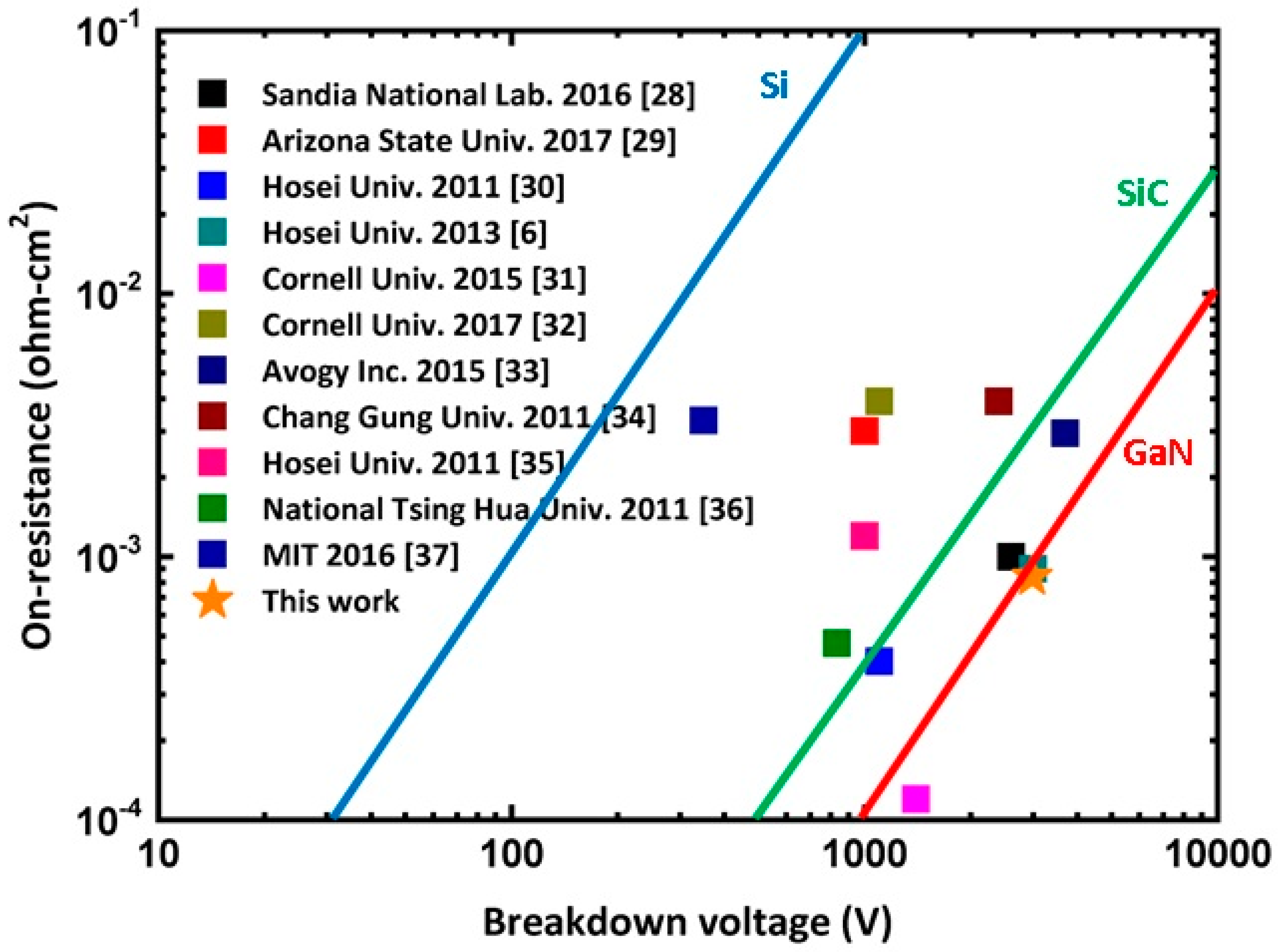
:1. Introduction
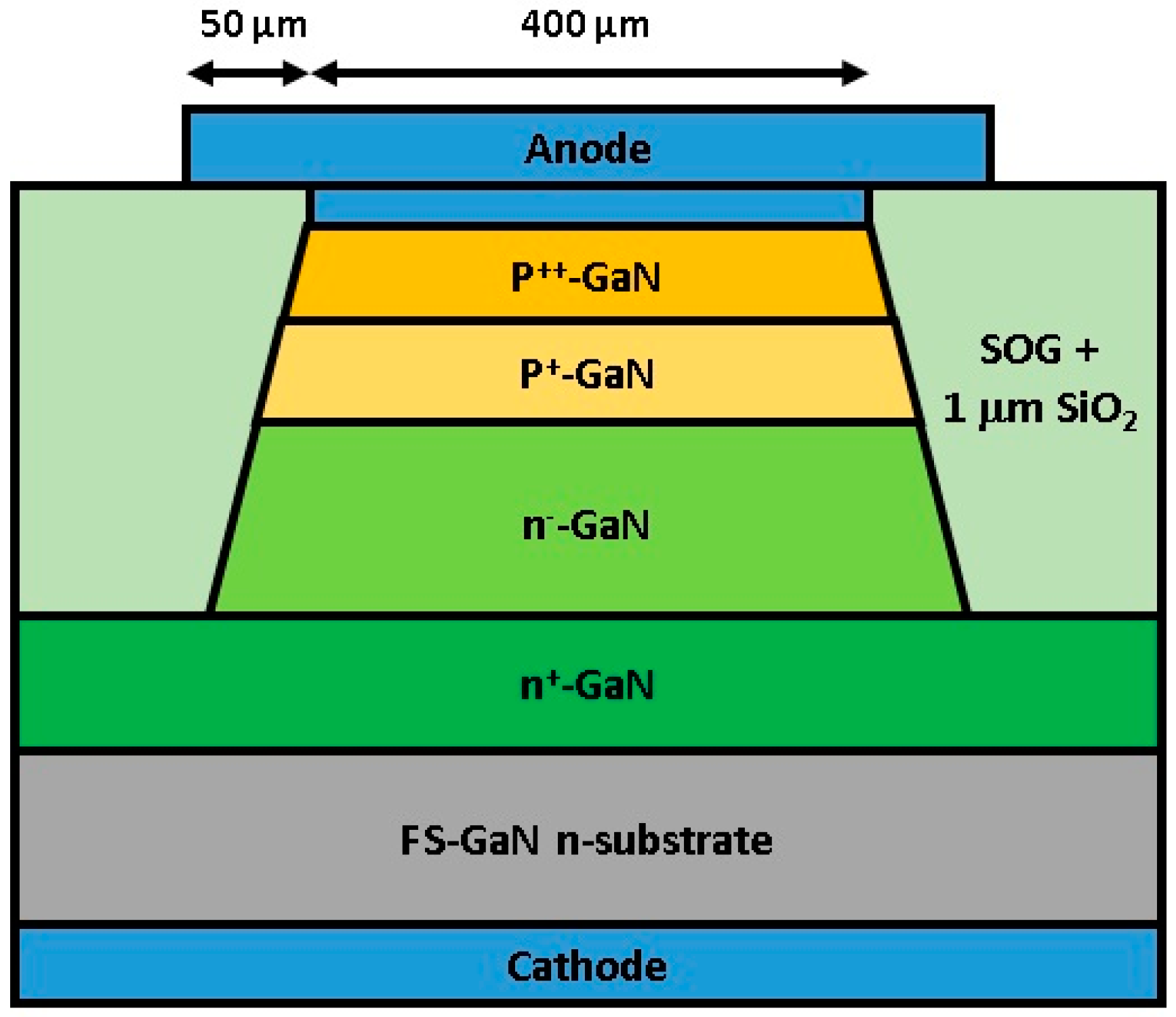
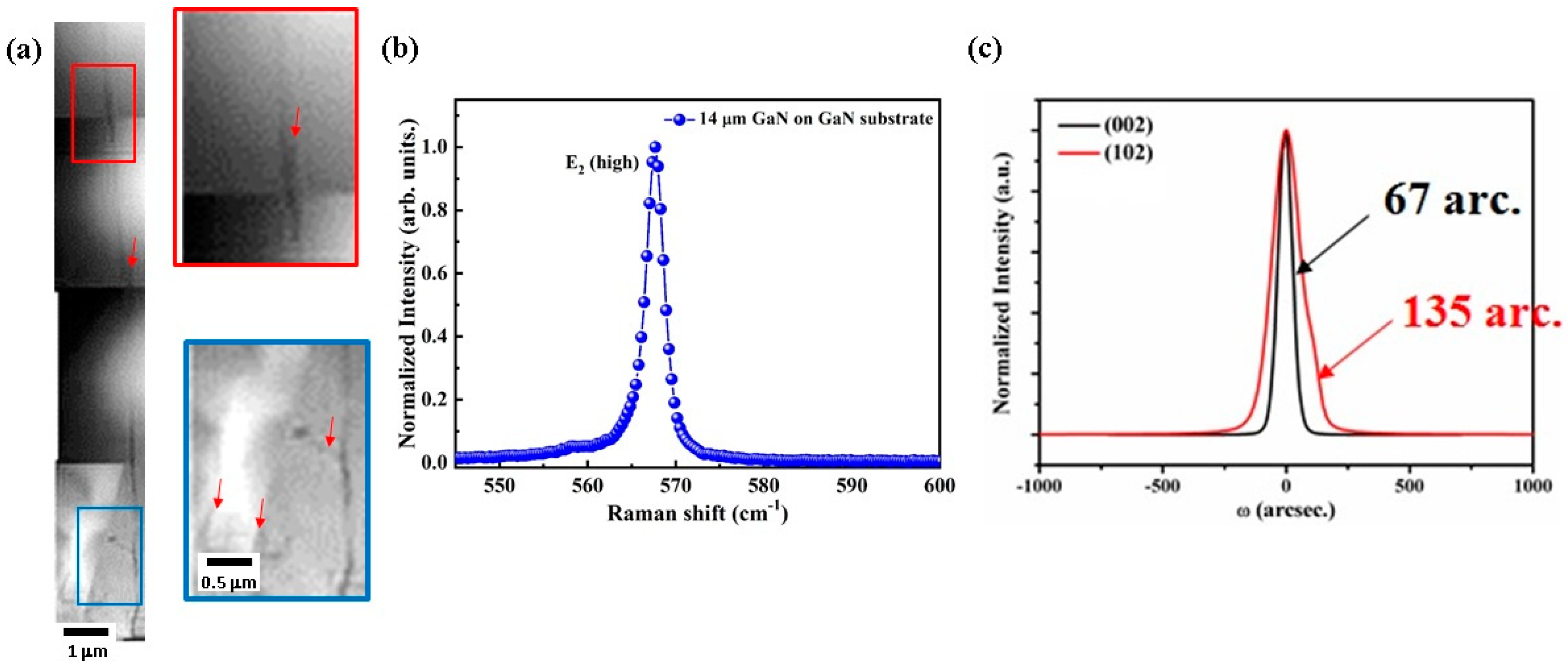
2. Experimental Section
2.1. Device Fabrication
2.2. Device Simulations
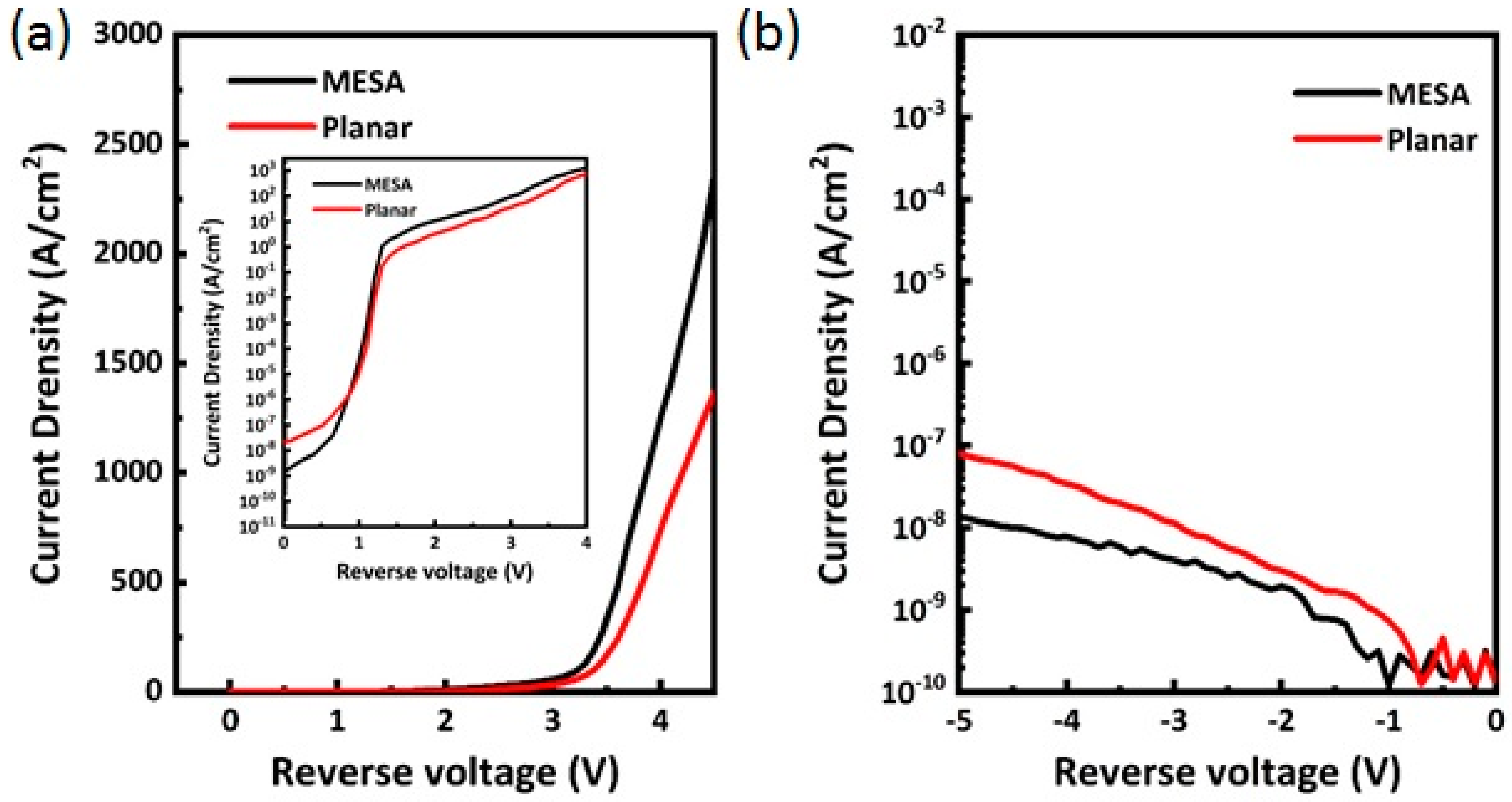
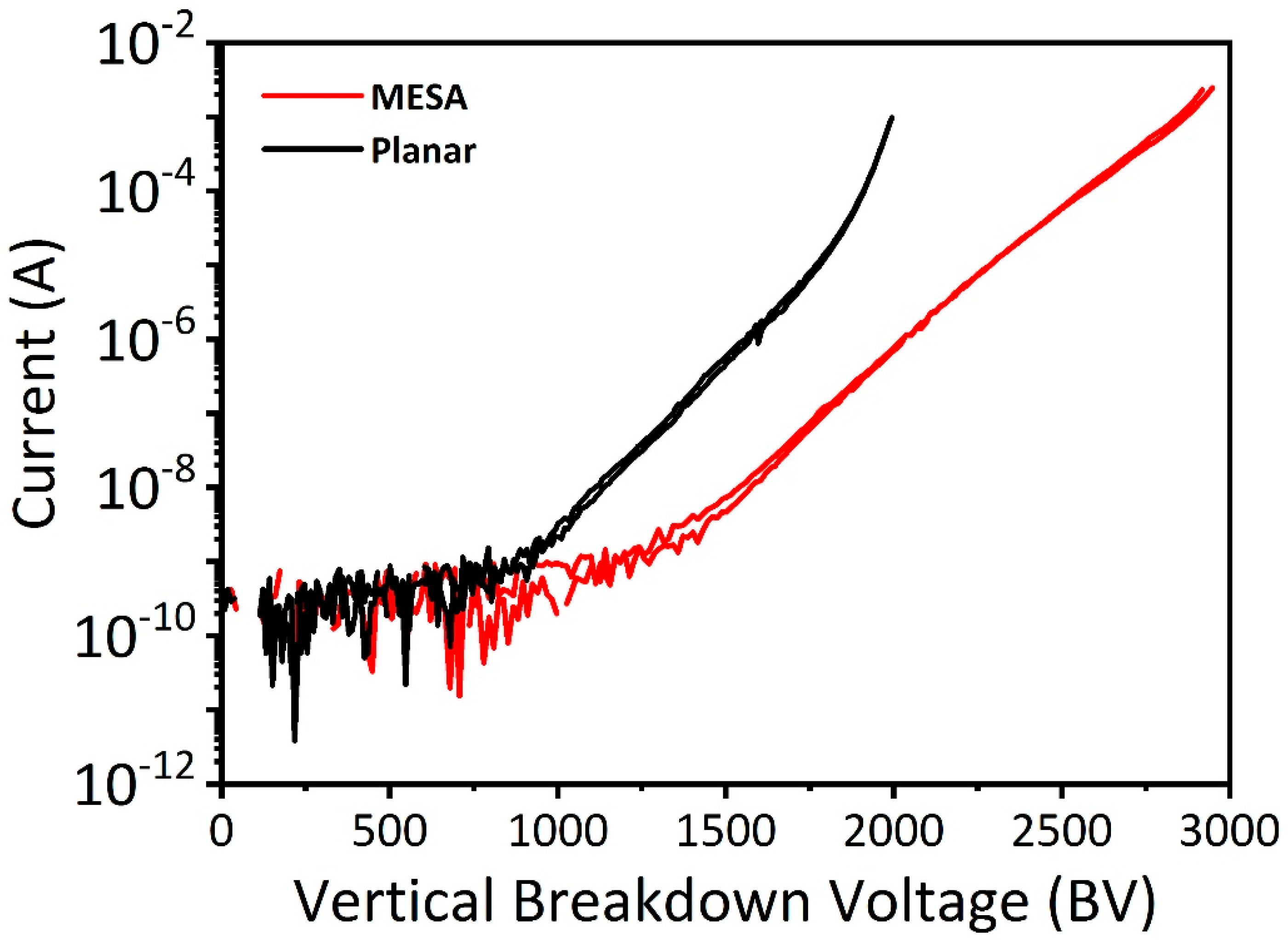
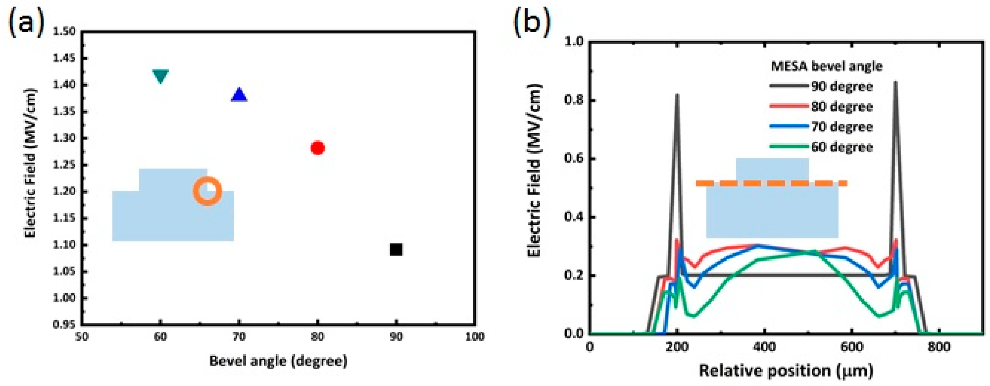
3. Results and Discussion
4. Summary
Author Contributions
Funding
Conflicts of Interest
References
- Mishra, U.K.; Parikh, P.; Wu, Y.F. AlGaN/GaN HEMTS: An overview of device operation and applications. Proc. IEEE 2002, 90, 1022–1031. [Google Scholar] [CrossRef] [Green Version]
- Chow, T.P.; Tyagi, R. Wide bandgap compound semiconductors for superior highvoltage unipolar power devices. IEEE Trans. Electron Devices 1994, 41, 1481–1483. [Google Scholar] [CrossRef]
- Liu, X.; Liu, Q.; Wang, J.; Yu, W.; Ao, J.P. 1.2 kV GaN Schottky barrier diodes on free-standing GaN wafer using a CMOS-compatible contact material. Jpn. J. Appl. Phys. 2017, 56, 026501. [Google Scholar] [CrossRef]
- Ohta, H.; Nakamura, T.; Mishima, T. High quality free-standing GaN substrates and their application to high breakdown voltage GaN p-n diodes. In Proceedings of the 2016 IEEE International Meeting for Future of Electron Devices, San Francisco, CA, USA, 3–7 December 2016; pp. 23–26. [Google Scholar]
- Nomoto, K.; Hu, Z.; Song, B.; Zhu, M.; Qi, M.; Yan, R.; Protasenko, V.; Imhoff, E.; Kuo, J.; Kaneda, N.; et al. GaN-on-GaN p-n power diodes with 3.48 kV and 0.95 mΩ-cm2: A record high figure-of-merit of 12.8 GW/cm2. In Proceedings of the 2015 IEEE International Electron Devices Meeting (IEDM), Washington, DC, USA, 7–9 December 2015. [Google Scholar]
- Hatakeyama, Y.; Nomoto, K.; Terano, A.; Kaneda, N.; Tsuchiya, T.; Mishima, T.; Nakamura, T. High-breakdown-voltage and low-specific-on-resistance GaN p-n junction diodes on free-standing GaN substrates fabricated through low-damage field-plate process. Jpn. J. Appl. Phys. 2013, 52, 2441–2452. [Google Scholar] [CrossRef]
- Chang, Y.F.; Liao, C.L.; Zheng, B.S.; Liu, J.Z.; Ho, C.L.; Hsieh, K.C.; Wu, M.C. Using two-step mesa to prevent the effects of sidewall defects on the GaN p-i-n diodes. IEEE J. Quantum Electron. 2015, 51, 8300106. [Google Scholar] [CrossRef]
- Carlile, R.N.; Liang, V.C.; Palusinski, O.A.; Smadi, M.M. Trench Etches in Silicon with Controllable Sidewall Angles. J. Electrochem. Soc. 1988, 135, 2058–2064. [Google Scholar] [CrossRef]
- Baliga, B.J. Gallium nitride devices for power electronic applications. Semicond. Sci. Technol. 2013, 28, 074011. [Google Scholar] [CrossRef]
- Rezaei, B.; Asgari, A.; Kalafi, M. Electronic band structure pseudopotential calculation of wurtzite III-nitride materials. Phys. B Condens. Matter 2006, 371, 107–111. [Google Scholar] [CrossRef]
- Mohammad, S.N.; Morkoç, H. Progress and prospects of group-III nitride semiconductors. Prog. Quantum Electron. 1996, 20, 361–525. [Google Scholar] [CrossRef]
- Suzuki, M.; Uenoyama, T.; Yanase, A. First-principles calculations of effective-mass parameters of AlN and GaN. Phys. Rev. B 1995, 52, 8132. [Google Scholar] [CrossRef] [PubMed]
- Santic, B. On the hole effective mass and the free hole statistics in wurtzite GaN. Semicond. Sci. Technol. 2003, 18, 219. [Google Scholar]
- Vurgaftman, I.; Meyer, J.Á.; Ram-Mohan, L.Á. Band parameters for III–V compound semiconductors and their alloys. J. Appl. Phys. 2001, 89, 5815–5875. [Google Scholar] [CrossRef] [Green Version]
- Götz, W.; Johnson, N.; Chen, C.; Liu, H.; Kuo, C.; Imler, W. Activation energies of Si donors in GaN. Appl. Phys. Lett. 1996, 68, 3144–3146. [Google Scholar] [CrossRef]
- Kumar, M.; Bhat, T.N.; Roul, B.; Rajpalke, M.K.; Kalghatgi, A.; Krupanidhi, S. Carrier concentration dependence of donor activation energy in n-type GaN epilayers grown on Si (1 1 1) by plasma-assisted MBE. Mater. Res. Bull. 2012, 47, 1306–1309. [Google Scholar] [CrossRef]
- Podor, B. Thermal ionization energy of Mg acceptors in GaN: Effects of doping level and compensation. In Proceedings of the International Conference on Solid State Crystals 2000: Growth, Characterization, and Applications of Single Crystals, Zakopane, Poland, 9–12 October 2001; Volume 4412, pp. 299–303. [Google Scholar]
- Yu, E.; Dang, X.; Asbeck, P.; Lau, S.; Sullivan, G. Spontaneous and piezoelectric polarization effects in III–V nitride heterostructures. J. Vac. Sci. Technol. B 1999, 17, 1742–1749. [Google Scholar] [CrossRef] [Green Version]
- Bernardini, F.; Fiorentini, V.; Vanderbilt, D. Accurate calculation of polarization-related quantities in semiconductors. Phys. Rev. B 2011, 63, 193201. [Google Scholar] [CrossRef] [Green Version]
- Farahmand, M.; Garetto, C.; Bellotti, E.; Brennan, K.F.; Goano, M.; Ghillino, E.; Ghione, G.; Albrecht, J.D.; Ruden, P.P. Monte Carlo simulation of electron transport in the III-nitride wurtzite phase materials system: Binaries and ternaries. IEEE Trans. Electron Devices 2001, 48, 535–542. [Google Scholar] [CrossRef] [Green Version]
- Schwierz, F. An electron mobility model for wurtzite GaN. Solid State Electron. 2005, 49, 889–895. [Google Scholar] [CrossRef]
- Mnatsakanov, T.T.; Levinshtein, M.E.; Pomortseva, L.I.; Yurkov, S.N.; Simin, G.S.; Khan, M.A. Carrier mobility model for GaN. Solid State Electron. 2003, 47, 111–115. [Google Scholar] [CrossRef]
- Sakowski, K.; Marcinkowski, L.; Krukowski, S.; Grzanka, S.; Litwin-Staszewska, E. Simulation of trap-assisted tunneling effect on characteristics of gallium nitride diodes. J. Appl. Phys. 2012, 111, 123115. [Google Scholar] [CrossRef]
- Pearton, S.J.; Abernathy, C.R.; Ren, F. Gallium Nitride Processing for Electronics, Sensors and Spintronics; Springer Science Business Media: Berlin, Germany, 2006. [Google Scholar]
- Puech, P.; Demangeot, F.; Frandon, J.; Pinquier, C.; Kuball, M.; Domnich, V.; Gogotsi, Y. GaN nanoindentation: A micro-Raman spectroscopy study of local strain fields. J. Appl. Phys. 2004, 96, 2853. [Google Scholar] [CrossRef]
- Chiu, C.H.; Li, Z.Y.; Chao, C.L.; Lo, M.H.; Kuo, H.C.; Yu, P.C.; Lu, T.C.; Wang, S.C.; Lau, K.M.; Cheng, S.J. Efficiency enhancement of UV/blue light emitting diodes via nanoscaled epitaxial lateral overgrowth of GaN on a SiO2 nanorod-array patterned sapphire substrate. J. Cryst. Growth 2008, 310, 5170. [Google Scholar] [CrossRef]
- Heinke, H.; Kirchner, V.; Einfeldt, S.; Hommel, D. X-ray diffraction analysis of the defect structure in epitaxial GaN. Appl. Phys. Lett. 2000, 77, 2145. [Google Scholar] [CrossRef]
- Dickerson, J.R.; Allerman, A.A.; Bryant, B.N.; Fischer, A.J.; King, M.P.; Moseley, M.W.; Armstrong, A.M.; Kaplar, R.J.; Kizilyalli, I.C.; Aktas, O.; et al. Vertical GaN power diodes with a bilayer edge termination. IEEE Trans. Electron Devices 2015, 63, 419–425. [Google Scholar] [CrossRef]
- Fu, H.; Huang, X.; Chen, H.; Lu, Z.; Zhang, X.; Zhao, Y. Effect of buffer layer design on vertical GaN-on-GaN pn and Schottky power diodes. IEEE Electron Device Lett. 2017, 38, 763–766. [Google Scholar] [CrossRef]
- Hatakeyama, Y.; Nomoto, K.; Kaneda, N.; Kawano, T.; Mishima, T.; Nakamura, T. Over 3.0 GW/cm2 Figure-of-Merit GaN pn Junction Diodes on Free-Standing GaN Substrates. IEEE Electron Device Lett. 2011, 32, 1674–1676. [Google Scholar] [CrossRef]
- Hu, Z.; Nomoto, K.; Song, B.; Zhu, M.; Qi, M.; Pan, M.; Gao, X.; Protasenko, V.; Jena, D.; Xing, H.G. Near unity ideality factor and Shockley-Read-Hall lifetime in GaN-on-GaN pn diodes with avalanche breakdown. Appl. Phys. Lett. 2015, 107, 243501. [Google Scholar] [CrossRef] [Green Version]
- Monavarian, M.; Pickrell, G.; Aragon, A.A.; Stricklin, I.; Crawford, M.H.; Allerman, A.A.; Celio, K.C.; Léonard, F.; Talin, A.A.; Armstrong, A.M.; et al. 1.1-kV vertical GaN pn diodes with p-GaN regrown by molecular beam epitaxy. IEEE Electron Device Lett. 2017, 38, 1071–1074. [Google Scholar]
- Kizilyalli, I.C.; Edwards, A.P.; Aktas, O.; Prunty, T.; Bour, D. Vertical power pn diodes based on bulk GaN. IEEE Trans. Electron Devices 2014, 62, 414–422. [Google Scholar] [CrossRef]
- Liu, X.; Chiu, H.C.; Wang, H.Y.; Hu, C.; Wang, H.C.; Kao, H.S.; Chien, F.T. 2.4 kV Vertical GaN PN Diodes on Free Standing GaN Wafer Using CMOS-Compatible Contact Materials. IEEE J. Electron Devices Soc. 2018, 6, 825–829. [Google Scholar] [CrossRef]
- Nomoto, K.; Hatakeyama, Y.; Katayose, H.; Kaneda, N.; Mishima, T.; Nakamura, T. Over 1.0 kV GaN p–n junction diodes on free-standing GaN substrates. Phys. Status Solidi A 2011, 208, 1535–1537. [Google Scholar] [CrossRef]
- Yu, C.J.; Lu, J.Y.; Shan, L.W.; Chen, C.J.; Liao, J.H.; Wu, M.C. Over 1 GW/cm2 for high-power GaN pin diodes with edge termination structure and laser annealing. J. Vac. Sci. Technol. B 2019, 37, 011208. [Google Scholar] [CrossRef]
- Zou, X.; Zhang, X.; Lu, X.; Tang, C.W.; Lau, K.M. Fully vertical GaN pin diodes using GaN-on-Si epilayers. IEEE Electron Device Lett. 2016, 37, 636–639. [Google Scholar] [CrossRef]


| Material Parameters | Values |
|---|---|
| Lattice constant (Å) | a = 3.192 c = 5.185 [10] |
| Dielectric constant | 8.9 [11] |
| Electron affinity (eV) | 4.5 [11] |
| Effective electron mass (m0) | 0.2 [12] |
| Conduction band density of state Nc (cm−3) | 2.3 × 10¹⁸ [12] |
| Effective hole mass (m0) | 1.25 [13] |
| Valence band density of state Nv (cm−3) | 3.5 × 10¹⁹ [12] |
| Critical breakdown field (MV/cm) | 3.5 [11] |
| Physical Phenomenon | Models | Parameters | Values |
|---|---|---|---|
| Bandgap | Temperature dependent bandgap model (@0K) | Reference bandgap (Eg0) | 3.53 eV [14] |
| Reference electron affinity (Chi0) | 4.1 eV [11] | ||
| Alpha | 9.09 × 10⁻⁴ eV/K | ||
| Beta | 830 K | ||
| Incomplete ionization | Silicon (n-doped) [15] | Donor activation energy (ΔED) | 17 meV [15] |
| Constant (αn) | 3.4 × 10⁻⁹ eV-cm [16] | ||
| Magnesium (p-doped) [17] | Acceptor activation energy (ΔED) | 240 meV | |
| Constant (αp) | 3.14 × 10⁻⁸ eV-cm [17] | ||
| Bandgap narrowing | Jain-Roulston [16] | Constant (K) | 1.15 × 10⁻⁸ eV-cm [16] |
| Polarization | Spontaneous polarization [18] | Spontaneous Polarization (Psp) | −0.029 C/m [18] |
| Piezo-electric polarization [19] | Elastic constant (c13) | 68 GPa [19] | |
| Elastic constant (c33) | 354 GPa [19] | ||
| Piezoelectric coefficient(e31) | −0.34 C/m2 [19] | ||
| Piezoelectric coefficient(e33) | 0.62 C/m2 [19] | ||
| relax | 1 | ||
| Electron mobility | Low field doping-dependent Arora Model [20] | μmin | 115 cm2/V-s |
| μmax | 1800 cm2/V-s | ||
| α | 0.8 | ||
| Reference doping (Nref) | 7 × 1016 cm−3 | ||
| β1 | −1.5 | ||
| β2 | −1.5 | ||
| β3 | 3.02 [20] | ||
| β4 | 0.81 [20] | ||
| High field transferred electron effect model [21] | Ec | 1.7 × 10⁵ V-cm [21] | |
| n1 | 4.19 [21] | ||
| n2 | 0.885 [21] | ||
| a | 5.64 | ||
| Hole mobility | Low field doping-dependent Arora Model [22] | μmin | 12 cm2/V-s |
| μmax | 167 cm2/V-s | ||
| α | 2.0 [22] | ||
| Reference doping (Nref) | 3 × 1017 cm−3 | ||
| β1 | 2.0 | ||
| β2 | −2.34 | ||
| β3 | 0.869 | ||
| β4 | −2.311 | ||
| High field Caughey Thomas model | μh0 | 70 cm2/V-s | |
| Saturation velocity (vh,sat) | 7 × 106 cm-s−1 | ||
| β | 0.725 | ||
| Impact ionization | Electron impact ionization Coefficients [9] | an | 1.5 × 105 cm−1 [4.3] |
| bn | 1.41 × 10⁷ V-cm−1 [9] | ||
| Hole impact ionization Coefficients [9] | ap | 6.4 × 105 cm−1 [9] | |
| bp | 1.46 × 10⁷ V-cm−1 [9] | ||
| Radiative recombination | Radiative recombination constant | Crad | 1.1 × 10⁻¹⁰ cm3-s−1 [23] |
| SRH recombination | Constant lifetime | Electron lifetime (τn) | 0.7 × 10⁻⁹ s |
| Hole lifetime (τp) | 2 × 10⁻⁹ s | ||
| Auger recombination | Electron coefficient [24] | An | 3 × 10⁻³¹ cm6-s−1 [24] |
| Hole coefficient [24] | Ap | 3 × 10⁻³¹ cm6-s−1 [24] |
© 2020 by the authors. Licensee MDPI, Basel, Switzerland. This article is an open access article distributed under the terms and conditions of the Creative Commons Attribution (CC BY) license (http://creativecommons.org/licenses/by/4.0/).
Share and Cite
Ho, W.-C.; Liu, Y.-H.; Wu, W.-H.; Huang Chen, S.-W.; Tzou, J.; Kuo, H.-C.; Sun, C.-W. The Study of High Breakdown Voltage Vertical GaN-on-GaN p-i-n Diode with Modified Mesa Structure. Crystals 2020, 10, 712. https://doi.org/10.3390/cryst10080712
Ho W-C, Liu Y-H, Wu W-H, Huang Chen S-W, Tzou J, Kuo H-C, Sun C-W. The Study of High Breakdown Voltage Vertical GaN-on-GaN p-i-n Diode with Modified Mesa Structure. Crystals. 2020; 10(8):712. https://doi.org/10.3390/cryst10080712
Chicago/Turabian StyleHo, Wen-Chieh, Yao-Hsing Liu, Wen-Hsuan Wu, Sung-Wen Huang Chen, Jerry Tzou, Hao-Chung Kuo, and Chia-Wei Sun. 2020. "The Study of High Breakdown Voltage Vertical GaN-on-GaN p-i-n Diode with Modified Mesa Structure" Crystals 10, no. 8: 712. https://doi.org/10.3390/cryst10080712
APA StyleHo, W.-C., Liu, Y.-H., Wu, W.-H., Huang Chen, S.-W., Tzou, J., Kuo, H.-C., & Sun, C.-W. (2020). The Study of High Breakdown Voltage Vertical GaN-on-GaN p-i-n Diode with Modified Mesa Structure. Crystals, 10(8), 712. https://doi.org/10.3390/cryst10080712