Article

Residual Oxygen Effects on the Properties of MoS2 Thin Films Deposited at Different Temperatures by Magnetron Sputtering

College of Science, Changchun University of Science and Technology, Changchun 130013, China
*
Author to whom correspondence should be addressed.
Crystals 2021, 11(10), 1183; https://doi.org/10.3390/cryst11101183
Submission received: 1 September 2021 / Revised: 25 September 2021 / Accepted: 27 September 2021 / Published: 28 September 2021
(This article belongs to the Section Inorganic Crystalline Materials)

Abstract

:
Molybdenum disulfide (MoS2) thin films were deposited at different temperatures (150 °C, 225 °C, 300 °C, 375 °C, and 450 °C) on quartz glass substrates and silicon substrates using the RF magnetron sputtering method. The influence of deposition temperature on the structural, optical, electrical properties and deposition rate of the obtained thin films was investigated by X-ray diffraction (XRD), Energy Dispersive Spectrometer (EDS), Raman, absorption and transmission spectroscopies, a resistivity-measuring instrument with the four-probe method, and a step profiler. It was found that the MoS2 thin films deposited at the temperatures of 150 °C, 225 °C, and 300 °C were of polycrystalline with a (101) preferred orientation. With increasing deposition temperatures from 150 °C to 300 °C, the crystallization quality of the MoS2 thin films was improved, the Raman vibrational modes were strengthened, the deposition rate decreased, and the optical transmission and bandgap increased. When the deposition temperature increased to above 375 °C, the molecular atoms were partially combined with oxygen atoms to form MoO3 thin film, which caused significant changes in the structural, optical, and electrical properties of the obtained thin films. Therefore, it was necessary to control the deposition temperature and reduce the contamination of oxygen atoms throughout the magnetron sputtering process.

1. Introduction

Molybdenum disulfide (MoS2) belongs to the transition metal dichalcogenides (TMDs). Structurally, MoS2 is a stack of planes where covalently bonded S-Mo-S atoms in layers are closely packed in a hexagonal arrangement by weak van der Waals forces. Because of its tunable energy band structure (1.8 eV for monolayer to 1.29 eV for bulk) [1] and unique photoelectric properties, MoS2 thin film has shown potential for preparation in the field of optoelectronic devices (e.g., detectors [2] and supercapacitors [3]) in recent years. As the basis for the manufacture of molybdenum disulfide-based devices, the preparation of their high-quality films is particularly important. Among all the methods for synthesizing molybdenum disulfide film, magnetron sputtering has become the mainstream synthesis method due to its advantages of simple process flow [4], fast deposition speed [5], and low damage to the film layer [6]. While research on magnetron sputtering of large-scale prepared molybdenum disulfide films has been gradually completed in recent years [7,8], studies on the influence of process parameters on film properties are not yet complete.
Previously, the effects of sputtering power [9,10], sputtering pressure [11], and incident flux angles [12] on the synthesis of molybdenum disulfide films by magnetron sputtering have been reported, and the influence of sputtering temperature on the frictional properties of molybdenum disulfide films have also been discussed [13,14]. The effect of RF power variation on film thickness as well as resistivity was investigated by Park [9] et al. As the RF power increases, the film thickness increases from 100 nm to 240 nm, and its resistivity increases from 356 to 2006 Ω/sq. Zhong et al. [10] found that the change in RF power has a significant effect on the binding energy of Mo atoms. Gong et al. [11] suggested that the huge discrepancy in electronegativity between MoS2 molecules promotes film defects at different deposition pressures, which in turn causes changes in the bandgap. They also pointed out that the optimal pressure for sputtering is 1.0 Pa. Li et al. [12] continued to investigate the effect of incident angular flux on molybdenum disulfide films deposited by magnetron sputtering and found that the structure of MoS2 films changed significantly with the variation of incident angular flux. Spalvins [15] deposited MoS2 films on aluminum and nickel substrates and investigated the different morphologies of the films at 150 °C and 320 °C, respectively. Until now, investigations into the effect of deposition temperature on molybdenum disulfide films have mainly focused on the changes of film morphology, while the structural and optoelectronic properties of the films have been less studied, as well as the deposition temperature settings not being very high (mostly below 350 °C). Since the ratio of S to Mo in MoS2 films synthesized by magnetron sputtering is far from 2, Chen et al. [16] suggested that the increase in substrate temperature decreases the stoichiometric ratio of Mo to S. The sublimation of S at high temperatures leads to the presence of a large number of vacancy defects within the film [17]. Changes in deposition temperature affect the binding of defects to impurity elements in the films [18,19,20,21] (e.g., oxygen), and the formation of impurities in the films can change their original properties. To improve the process preparation of molybdenum disulfide to expand its application in the device field, it is essential to study the effect of high temperature on the optoelectronic and structural properties of molybdenum disulfide prepared by magnetron sputtering.
In this work, MoS2 thin films were synthesized at different sputtering temperatures. The effects of sputtering temperature on the structure, optical and electrical properties, and deposition rate of the obtained films were investigated to provide a reference for the preparation of high-quality films with excellent properties.

2. Materials and Methods

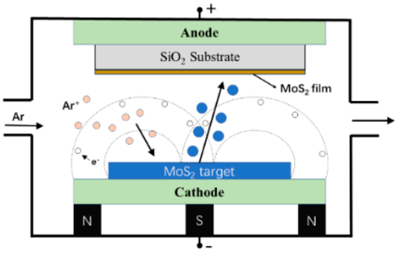
2.1. Preparation of Molybdenum Disulfide Film

In view of the application of MoS2-based devices, their application is more useful for MoS2 thin films deposited on the silicon substrate. However, silicon substrates are opaque and non-insulating, thus, it would be difficult to investigate the optical and electrical properties of MoS2 thin films in our experiments. In this paper, the quartz glass substrate was simultaneously used in our experiment to investigate the optical and electrical properties of MoS2 thin films. Before sputtering, the quartz glass substrates and silicon substrates were ultrasonically cleaned in acetone, alcohol, and deionized water and dried in nitrogen gas. MoS2 films were grown on the substrates by the radio frequency (RF) sputtering method. To investigate the effect of deposition temperature on the film growth, the control temperatures were 150 °C, 225 °C, 300 °C, 375 °C, and 450 °C, respectively. MoS2 ceramic target (99.99% purity) and argon (99.9% purity) were used as the sputtering target and sputtering gas, respectively. The argon flow rate was maintained at 10 sccm by a mass flow meter. The system was pumped to a base pressure of 3 × 10⁻⁴ Pa before sputtering. During sputtering, the pressure was maintained at 1.0 Pa, the distance between substrate and target was controlled at 7.5 cm, while the RF power was 80 W. Sputtering time was 30 min. After the sputtering process, the heater and argon gas pipeline were turned off, then the sample was naturally cooled to room temperature and removed for use. The principle of sputtering deposition was shown in Figure 1.

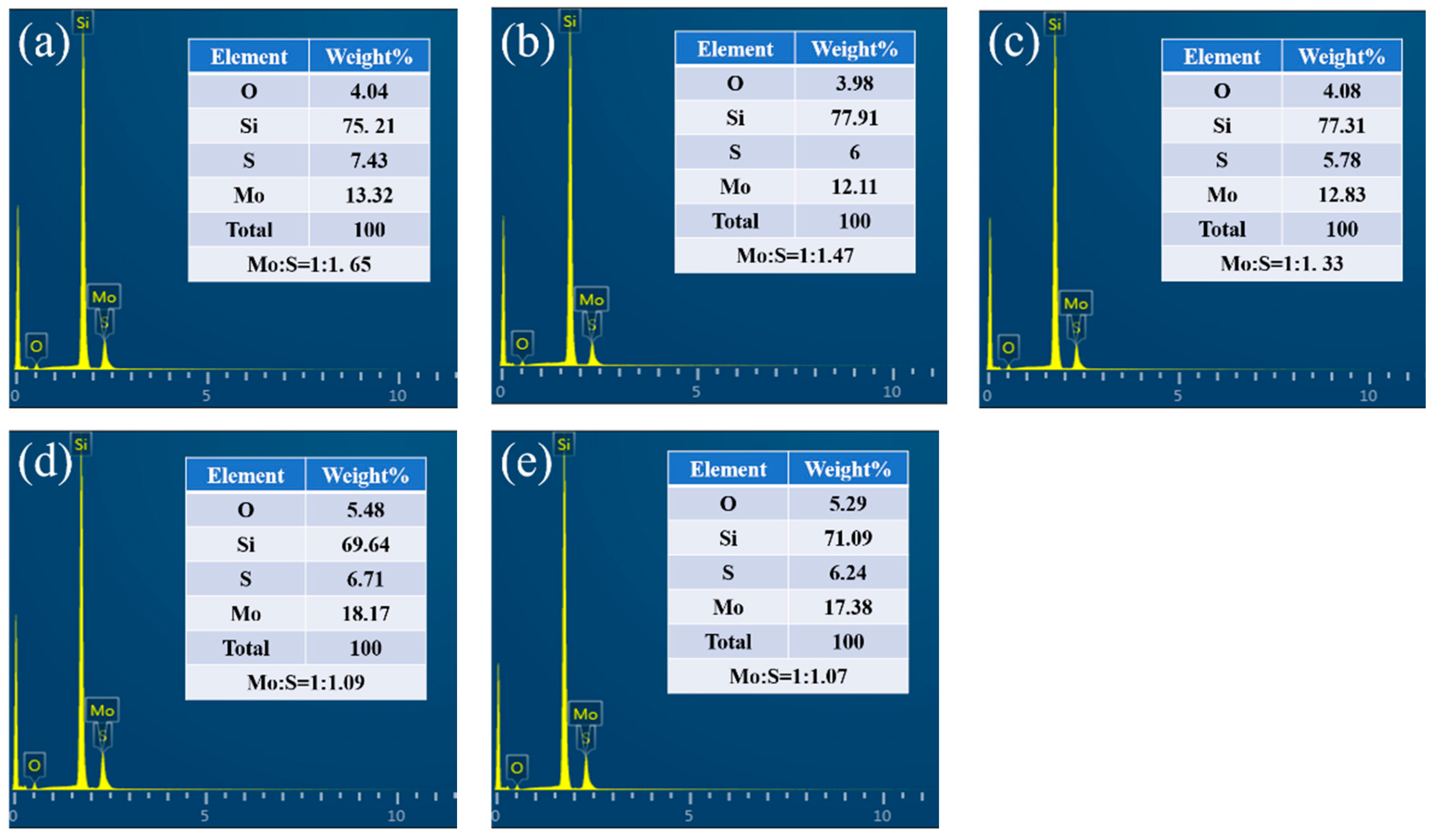
2.2. Characterization of Properties

The properties such as crystal orientation of MoS2 thin films were measured by X-ray diffractometer with a ray wavelength of 0.15418 nm. The Raman spectra of the samples were measured by a Raman spectrophotometer with a laser wavelength of 532 nm. The absorption and transmission spectra of the films were measured between 400 nm to 800 nm by a double-beam UV-vis spectrophotometer. The thicknesses of different samples were measured with a step meter. The resistivity of the films was measured with a four-probe resistance tester.

3. Results and Discussion

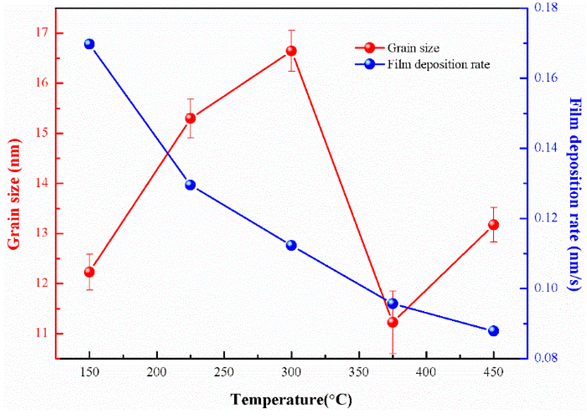
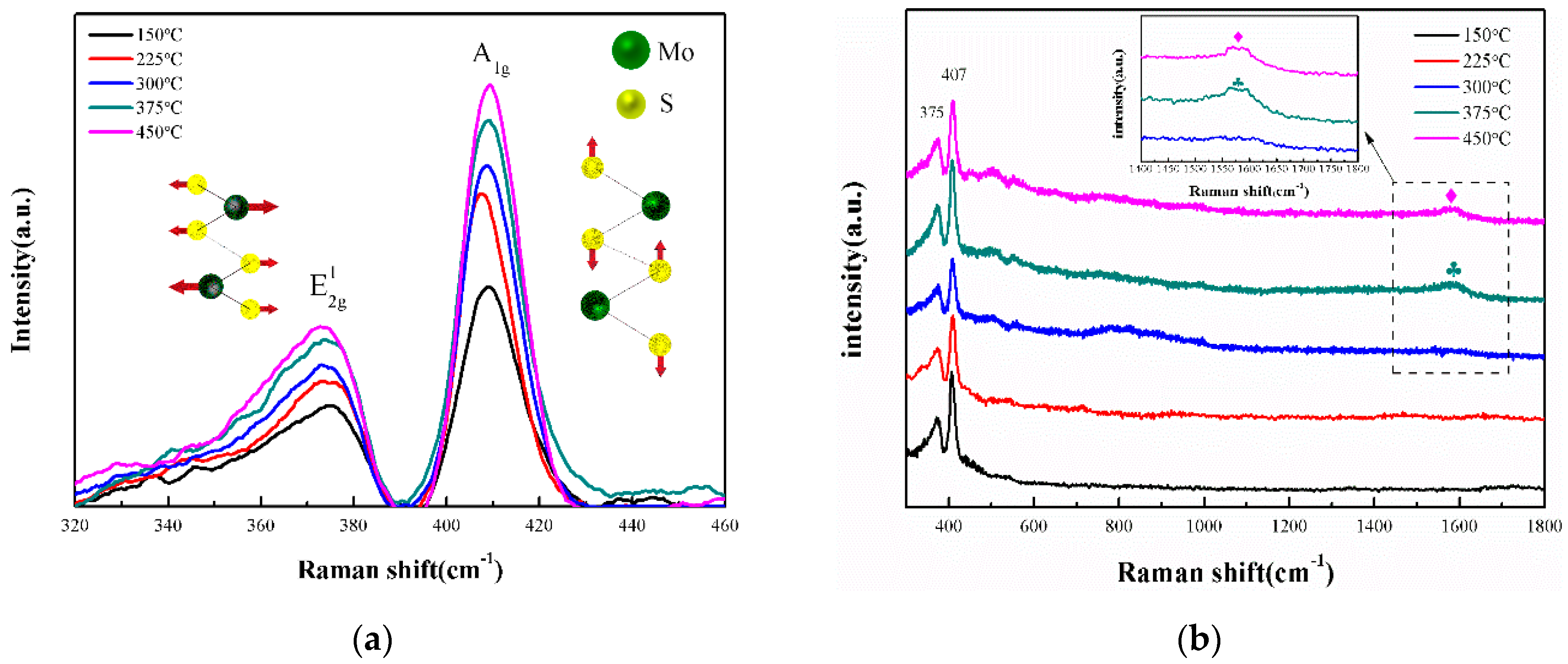
3.1. Structure of the Films

Figure 2 shows the X-ray diffraction results of the obtained thin films grown at different temperatures (150 °C, 225 °C, 300 °C, 375 °C, and 450 °C). From this figure, it can be seen that there was a notable diffraction peak that appeared at 33.5° for all the samples grown at different temperatures. According to the Standard Powder Diffraction File (JCPDS:37-1492), this peak was (101) diffraction peak for 2H-MoS2 material, proving that the obtained MoS2 thin film was of polycrystalline with (101) preferred orientation. It can also be seen from this figure that the samples grown at 375 °C and 450 °C had a diffraction peak of high intensity at 12.7°. This peak was a (020) diffraction peak from MoO3 material according to the Standard Powder Diffraction File (JCPDS:05-0508). To verify our speculation, the elemental composition of molybdenum disulfide films grown on silicon substrates was analyzed using an energy dispersive spectrometer (EDS), and the results are shown in Figure 3. A clear peak of silicon elements can be observed from the figure, which was due to our choice of MoS2 films grown on silicon substrates as the sample for testing. Based on the EDS data, the stoichiometric ratio of Mo and S in the prepared MoS2 films was calculated to be less than 1:2, and it was found that the Mo and S stoichiometric ratio decreased gradually with the increase in temperature, which was in line with the previous conclusions of Chen et al. [16]. It was also found that when the deposition temperature was not higher than 300 °C, the percentage of O elements in the films was about 4%, which was in a relatively small variation range. When the deposition temperature was higher than 300 °C, the percentage of O elements in the films increased by more than 1%. Combined with the XRD result, we concluded that when the deposition temperature was higher than 300 °C, oxygen atoms replace S vacancies in the MoS2 films and combined with Mo atoms to form Mo-O chemical bonds, which in turn led to the generation of MoO3 impurities. The formation of Mo-O chemical bonds allowed more Mo atoms to be immobilized inside the lattice during deposition, while the evaporation of S is not mitigated so that the stoichiometric ratio of Mo and S decreased significantly in the samples at 375 °C versus 450 °C compared to those at temperatures below 300 °C. Comparing the results with other experiments (the XRD results of the sample by Nikpay et al. [22] and Duan et al. [23]), it was found that molybdenum oxide impurities did not appear in the films when the substrate temperature was below 300 °C, confirming the reliability of our conclusions.
The average grain size (including all peaks) of the MoS2 could be deduced from the Scherrer equation [24]:
D = K γ β cos θ
where D represents the average grain size; K is the Scherrer constant (0.89);   γ means the wavelength of X-rays (0.15406 nm); β denotes the full width at half maxima (FWHM) of the sample diffraction peak; θ indicates the Bragg diffraction angle. The deposition rate of films with different sputtering temperatures could be calculated from the thickness of the film and the deposition time (30 min); the thickness of the obtained samples was measured using a step profiler, and the results are given in Table 1. The average grain size and film deposition rate of MoS2 films deposited at different temperatures are shown in Figure 4. There was a 5% to 8% deviation in the calculated average grain size, but this did not affect the trend of the result variation. It was shown that the deposition rate of thin films decreased with the increase in temperature. The grain size became gradually larger with increasing temperature when the deposition temperature was below 300 °C, but this trend changed when the deposition temperature was higher than 300 °C. From the results, it was found that the generation of Mo oxides during high-temperature deposition changed the trend of grain size variation with deposition temperature. Cui et al. and Zhong et al. [25,26] found that MoO3 diffraction peaks appeared in the MoS2 samples through the calcination method when the calcination temperature exceeded 300 °C, and the generation of MoO3 had a great influence on the absorption spectrum of MoS2 nanoplates. Liu et al. [27] investigated the evolutions of morphology and electronic properties of the MoS2 layer exposed to ultraviolet ozone. It was found that inhomogeneous oxidation in MoS2 thin films can significantly change the optoelectronic properties of MoS2 thin films. It is believed that the oxidation of MoS2 thin films deposited by magnetron sputtering in our experiment would also affect the other properties of the films, which is discussed in the following section.
As a popular and non-destructive technique to investigate the microstructure of thin films, Raman spectroscopy with a 532 nm laser line was used to further characterize the MoS2 films deposited at different temperatures, and the results are shown in Figure 5. From this figure, it can be seen that there were two prominent peaks centered at around 375 cm−1 and 407 cm−1, which correspond to the E 2 g 1 and A1g vibrational modes of the Raman spectrum of MoS2 films, respectively. In the E 2 g 1 mode, Mo and S atoms oscillated in an anti-phase parallel to the crystal plane; therefore, E 2 g 1 involved the vibration of Mo and S atoms in the basal plane. In the A1g mode, S atoms oscillated in anti-phase perpendicular to the surface plane, and Mo atoms remained fixed as shown in Figure 5a [28,29,30]. The wavenumber difference Δk between the peaks corresponds to the film thickness of the MoS2 film. Samples with Δk values close to 18–20 cm−1 correspond to monolayer MoS2, and the value increased with the thickness of the film [31,32]. The average value of Δk for our five experimental samples was 34.38 cm−1 (150 °C: 32.6 cm−1; 225 °C: 33.5 cm−1; 300 °C: 34.8 cm−1; 375 °C: 35.3 cm−1; 450 °C: 35.7 cm−1), with an error of 0.38 cm−1 from the standard bulk molybdenum disulfide Δk (34 cm−1), which corresponds to a thickness close to the standard of bulk MoS2, indicating that the prepared film samples are thicker in layers. By comparing the five curves in Figure 5a, it was found that the intensities of both the E 2 g 1 and A1g Raman peaks increased with the increase in the deposition temperature. Analyzing the XRD and Raman spectra together proved that higher deposition temperature (150–300 °C) was beneficial to improve the crystallization quality of the MoS2 films. In Figure 5b, in addition to the two peaks of E 2 g 1 and A1g, a tiny peak near 1580 cm−1 was found for the samples deposited at 375 °C and 450 °C, respectively. Combining previous literature [33,34,35] and the results of XRD and EDS (Figure 2 and Figure 3), the appearance of this weak peak is considered to be related to the formation of Mo-O bonds in the films.

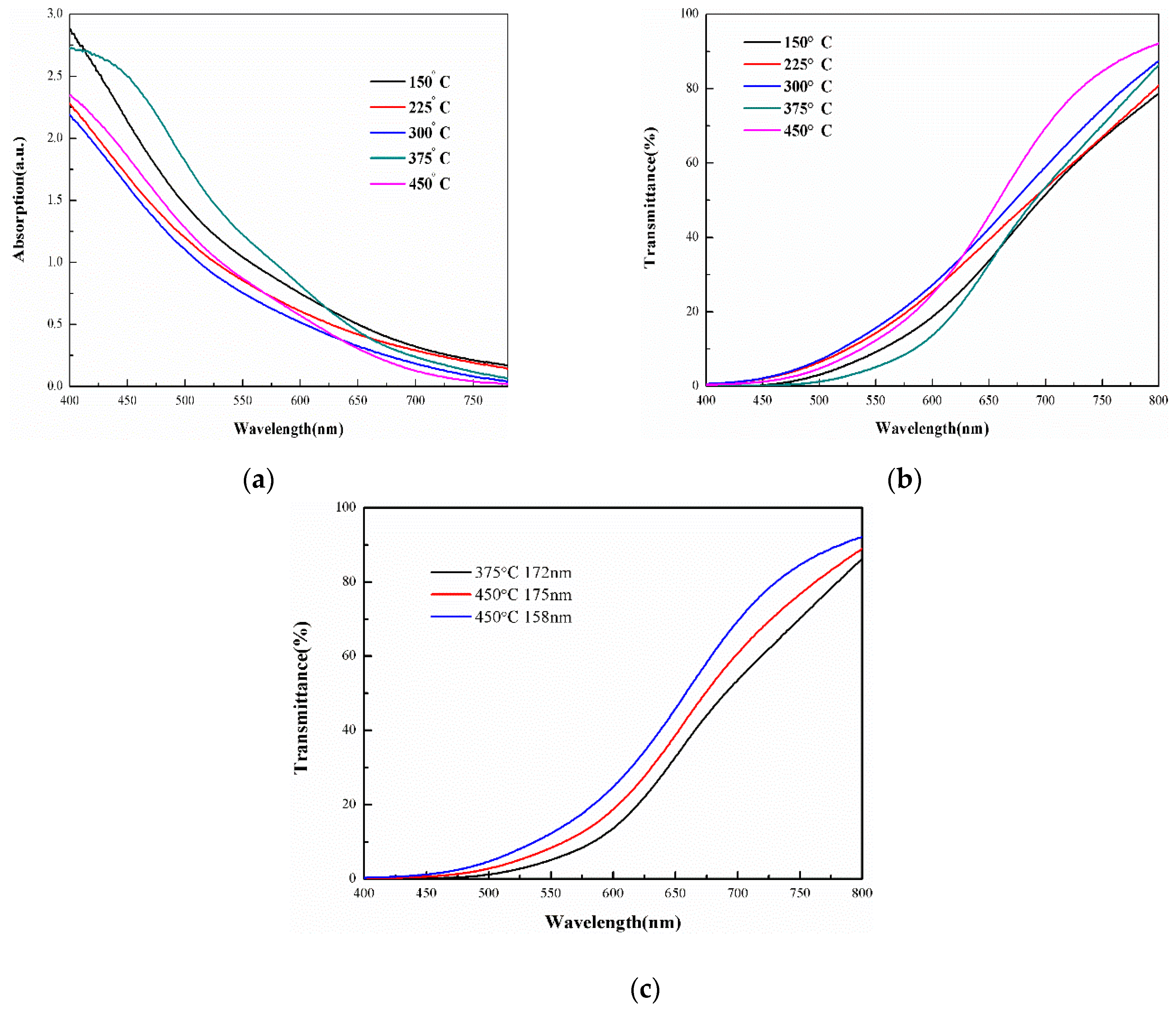
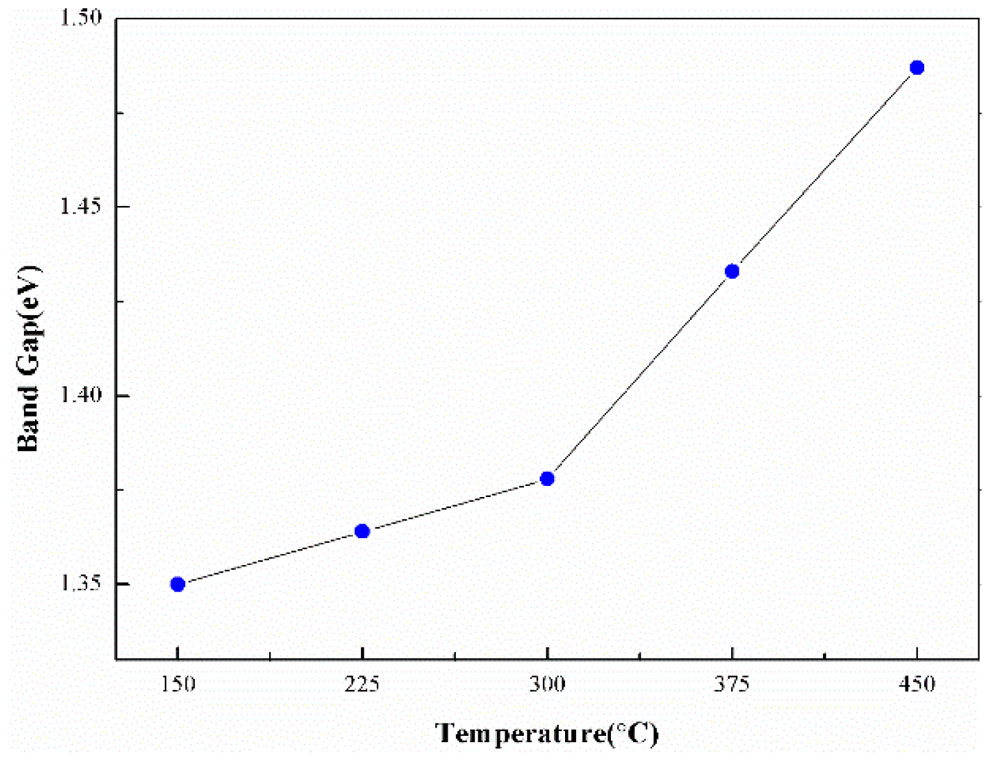
3.2. Optical Properties of the Films

Figure 6 shows the absorption and transmission spectra of the MoS2 films for visible light at different deposition temperatures. From these plots, it was observed that when the deposition temperature was increased from 150 °C to 300 °C, the absorption decreased and the transmission increased. A regular trend of variation in the absorption and transmission curves was observed, which was due to the increase in temperature reducing the deposition rate of the film, thus decreasing the thickness of the film. When the deposition temperature was increased above 300 °C, the original variation pattern was broken, and the curves for the 375 °C and 450 °C samples crossed the previous curves. In order to investigate the changes in the transmittance spectrum for the samples deposited at higher temperatures (375 °C and 450 °C), in Figure 6b, an additional experiment was conducted. In this experiment, a MoS2 thin film with a thickness of 175 nm was deposited at the temperature of 450 °C by prolonging the deposition time. The thickness of 175 nm was close to that of the MoS2 sample (172 nm), deposited at 375 °C. The transmittance spectra for the three samples (172 nm deposited at 375 °C, 175 nm deposited at 450 °C, and 158 nm deposited at 450 °C, respectively) are shown in Figure 6c. It can be seen that the transmission for the sample deposition at 450 °C is higher than that deposited at 375 °C with almost the same thickness. Thus, it can be concluded that the changes in the transmittance spectrum for the samples deposited at higher temperatures (375 °C and 450 °C) were not only caused by the thickness of the MoS2 thin film, but also by the further formation of Mo-O bonds. As analyzed earlier, the formation of a large number of S vacancies and the presence of MoO3 in the film at high temperatures could dramatically change the optical properties of the film sample.
The optical band gap (Eg) of the samples can be calculated from the absorption spectra using the Tauc formula [36,37]:
( α h ν ) 1 / 2 = A ( h ν E g )
( α h ν ) 2 = A ( h ν E g )
where h ν represents the incident photon energy, and α denotes the absorption coefficient. The exponent of ( α hv) is taken as 1/2 when the calculated material is an indirect bandgap; when the calculated material is a direct bandgap, the exponent of α is taken as 2. To determine the type of bandgap of the MoS2 films, two sets of curves of the samples were made separately by different calculation methods. The optical band gaps of MoS2 films calculated by different methods are given in Figure 7a,b, respectively. Molybdenum disulfide is known to be a transition metal sulfide with a tunable bandgap (1.8 eV for the single layer with a direct bandgap; 1.29 eV for bulk with an indirect bandgap [38,39]), and the bandgap decreases with increasing thickness. The results obtained from the calculations shown in Figure 7b were not under the bandgap variation range of molybdenum disulfide, and the MoS2 bandgap values with 305 nm thickness were close to the standard 1.8 eV for a single layer, which was unacceptable. In contrast, the results are shown in Figure 7a were perfectly in line with the variation range of the bandgap of molybdenum disulfide, and the bandgap gradually increased with decreasing thickness, so the prepared MoS2 films had an indirect bandgap. The variation of the optical band gap of films with different deposition temperatures is shown in Figure 8. With the increasing deposition temperature from 150 °C to 300 °C, the optical band gap increased from 1.350 eV to 1.378 eV gradually; this was due to the decrease in the thickness of MoS2 thin films [1]. When the deposition temperature was raised to 375 °C, the optical band gap increased to 1.433 eV rapidly. At the temperature of 375 °C, the MoS2 thin film had partially changed into MoO3 thin film; the bandgap of MoO3 (3.1 eV) [40] was larger than that of MoS2, thus causing the increase in the bandgap of the obtained sample.

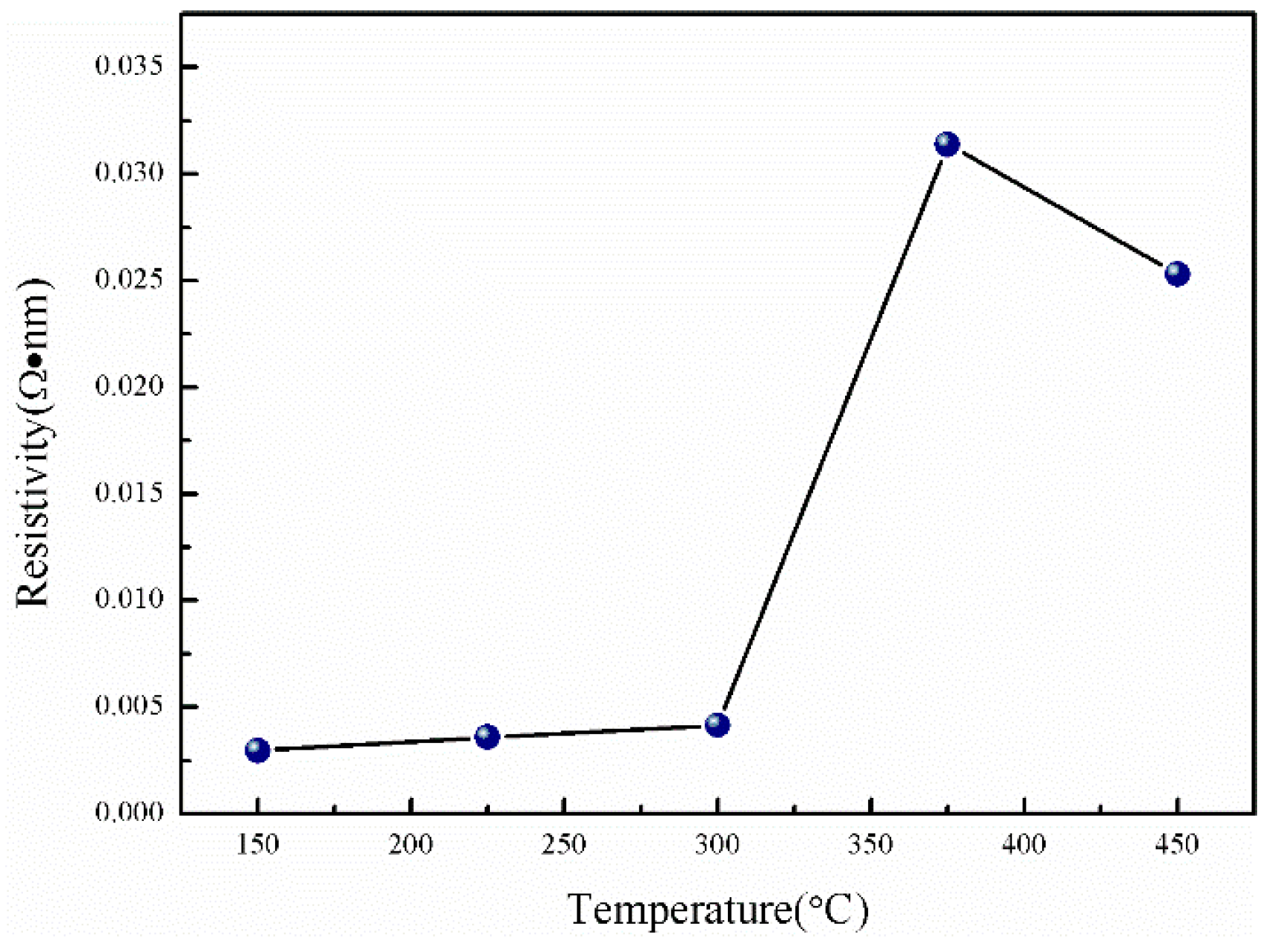
3.3. Electrical Properties of the Films

The resistivity of the obtained thin film was measured by a resistivity-measuring instrument with the four-probe method, and the results are shown in Figure 9. It was found the resistivity increased smoothly as the deposition temperature increased from 150 °C to 300 °C. When deposition temperature was raised to 375 °C, the resistivity was increased by one order. Further increased deposition temperatures resulted in a decrease in resistivity of about 20%. Combined with the results shown in Figure 3, it can be seen that there were a large number of S vacancy defects in the film. Qi et al. [41] pointed out that oxygen impurities play a crucial role in the transition from n-type to p-type conductivity of MoS2 films. It is well known that the pure MoS2 film with electrons as the main carriers is an n-type semiconductor. After combining the EDS results for analysis, we believe that when the sample deposition temperature was higher than 300 °C, the MoO3 impurities produced by O atoms intruding into the film to replace S vacancies changed the type of conductivity of MoS2 films, which is the reason for the abrupt change in the curve across orders of magnitude at 375 °C. This evidences that the formation of MoO3 in thin films greatly affects the electrical properties of thin films. As can be seen in Figure 9, the resistivity did not show a linear change after the abrupt change at 375 °C, but produced a decrease at 450 °C. This phenomenon is related to the rate of oxygen atom intrusion into the films at high temperatures and the number of S vacancies formed. The electrical conductivity of the films is related to the carrier concentration, electron mobility, and Hall effect of MoS2, the specific reasons of which we will continue to analyze in future experimental tests.

4. Conclusions

MoS2 thin films were grown successfully on quartz glass and silicon substrates by magnetron sputtering. It was found that the deposition temperature greatly influenced the structural, optical, and electrical properties of the obtained thin films. Below 300 °C, the obtained MoS2 thin films were polycrystalline with (101) preferred orientation and showed E 2 g 1 and A1g vibrational modes in the Raman spectrum. With the deposition temperature increasing from 150 °C to 300 °C, the crystal quality improved, the optical band gap and resistivity increased, and the thickness decreased. When the deposition temperature was over 375 °C, the molecular atoms were combined with the residual oxygen atoms to form MoO3. This oxidization process influenced the purity of the MoS2 thin films, thus causing great changes in the structural, optical, and electrical properties of the obtained thin films.

Author Contributions

Funding acquisition, X.W.; Investigation, P.W.; Resources, X.W.; Visualization, F.T.; Writing—original draft, P.W. and R.Z.; Writing—review and editing, P.W. and X.W. All authors have read and agreed to the published version of the manuscript.

Funding

This work was supported by the National Natural Science Foundation of China (No. 11874091).

Conflicts of Interest

The authors declare no conflict of interests with regard to the publication of this paper.

References

  1. Mak, K.F.; Lee, C.; Hone, J.; Shan, J.; Heinz, T.F. Atomically thin MoS2: A new direct-gap semiconductor. Phys. Rev. Lett. 2010, 105, 136805. [Google Scholar] [CrossRef] [Green Version]
  2. Xie, Y.; Zhang, B.; Wang, S.; Wang, D.; Wang, A.; Wang, Z.; Yu, H.; Zhang, H.; Chen, Y.; Zhao, M.; et al. Ultrabroadband MoS2 photodetector with spectral response from 445 to 2717 nm. Adv. Mater. 2017, 29, 1605972. [Google Scholar] [CrossRef]
  3. Choudhary, N.; Patel, M.; Ho, Y.H.; Dahotre, N.B.; Lee, W.; Hwang, J.Y.; Choi, W. Directly deposited MoS2 thin-film electrodes for high-performance supercapacitors. J. Mater. Chem. A 2015, 3, 24049–24054. [Google Scholar] [CrossRef]
  4. Musil, J.; Čiperová, Z.; Čerstvý, R.; Haviar, S. Flexible hard (Zr, Si) alloy films prepared by magnetron sputtering. Thin Solid Film. 2019, 688, 137216. [Google Scholar] [CrossRef]
  5. Petrov, I.; Hall, A.; Mei, A.B.; Nedfors, N.; Zhirkov, I.; Rosen, J.; Reed, A.; Howe, B.; Greczynski, G.; Birch, J.; et al. Controlling the boron-to-titanium ratio in magnetron-sputter-deposited TiBx thin films. J. Vac. Sci. Technol. A Vac. Surf. Film. 2017, 35, 050601. [Google Scholar] [CrossRef]
  6. Sidelev, D.V.; Krivobokov, V.P. Angular thickness distribution and target utilization for hot Ni target magnetron sputtering. Vacuum 2019, 160, 418–420. [Google Scholar] [CrossRef]
  7. Tao, J.; Chai, J.; Lu, X.; Wong, L.M.; Wong, T.I.; Pan, J.; Xiong, Q.; Chi, D.; Wang, S. Growth of wafer-scale MoS2 monolayer by magnetron sputtering. Nanoscale 2015, 7, 2497–2503. [Google Scholar] [CrossRef]
  8. Samassekou, H.; Alkabsh, A.; Wasala, M.; Eaton, M.; Walber, A.; Walker, A.; Pitkänen, O.; Kordas, K.; Talapatra, S.; Jayasekera, T.; et al. Viable route towards large-area 2D MoS2 using magnetron sputtering. 2D Mater. 2017, 4, 021002. [Google Scholar] [CrossRef] [Green Version]
  9. Park, J.; Kang, Y.C. Effect of Radio Frequency Power on the Physicochemical Properties of MoS2 Films Obtained by rf Magnetron Sputtering. Bull. Korean Chem. Soc. 2016, 37, 1326–1330. [Google Scholar] [CrossRef]
  10. Zhong, W.; Deng, S.; Wang, K.; Li, G.; Li, G.; Chen, R.; Kwok, H.S. Feasible route for a large area few-layer MoS2 with magnetron sputtering. Nanomaterials 2018, 8, 590. [Google Scholar] [CrossRef] [Green Version]
  11. Gong, C.; Xiao, J.; Zhu, L.; Wang, Z.; Ma, S. Effect of deposition pressure on the microstructure and optical bandgap of molybdenum disulfide films prepared by magnetron sputtering. Coatings 2019, 9, 570. [Google Scholar] [CrossRef] [Green Version]
  12. Qiao, L.; Wang, P.; Chai, L.; Zhang, X.; Liu, W. Influence of the incident flux angles on the structures and properties of magnetron sputtered MoS2 films. J. Phys. D Appl. Phys. 2015, 48, 175304. [Google Scholar] [CrossRef]
  13. Hamilton, M.A.; Alvarez, L.A.; Mauntler, N.A.; Argibay, N.; Colbert, R.; Burris, D.L.; Muratore, C.; Voevodin, A.A.; Perry, S.S.; Sawyer, W.G. A possible link between macroscopic wear and temperature-dependent friction behaviors of MoS2 coatings. Tribol. Lett. 2008, 32, 91–98. [Google Scholar] [CrossRef]
  14. Kubart, T.; Polcar, T.; Kopecký, L.; Novak, R.; Novakova, D. Temperature dependence of tribological properties of MoS2 and MoSe2 coatings. Surf. Coat. Technol. 2005, 193, 230–233. [Google Scholar] [CrossRef]
  15. Spalvins, T. Structure of sputtered molybdenum disulfide films at various substrate temperatures. ASLE Trans. 1974, 17, 1–7. [Google Scholar] [CrossRef]
  16. Chen, G.; Lu, B.; Cui, X.; Xiao, J. Effects of Deposition and Annealing Temperature on the Structure and Optical Band Gap of MoS2 Films. Materials 2020, 13, 5515. [Google Scholar] [CrossRef] [PubMed]
  17. Wang, P.; Qiao, L.; Xu, J.; Li, W.; Liu, W. Erosion mechanism of MoS2-based films exposed to atomic oxygen environments. ACS Appl. Mater. Interfaces 2015, 7, 12943–12950. [Google Scholar] [CrossRef]
  18. Buck, V. Preparation and properties of different types of sputtered MoS2 films. Wear 1987, 114, 263–274. [Google Scholar] [CrossRef]
  19. Zhou, Z.; Xu, T.; Zhang, C.; Li, S.; Xu, J.; Sun, L.; Gao, L. Enhancing stability by tuning element ratio in 2D transition metal chalcogenides. Nano Res. 2021, 14, 1704–1710. [Google Scholar] [CrossRef]
  20. Gao, J.; Li, B.; Tan, J.; Chow, P.; Lu, T.M.; Koratkar, N. Aging of transition metal dichalcogenide monolayers. ACS Nano 2016, 10, 2628–2635. [Google Scholar] [CrossRef]
  21. Serpini, E.; Rota, A.; Ballestrazzi, A.; Marchetto, D.; Gualtieri, E.; Valeri, S. The role of humidity and oxygen on MoS2 thin films deposited by RF PVD magnetron sputtering. Surf. Coat. Technol. 2017, 319, 345–352. [Google Scholar] [CrossRef]
  22. Nikpay, M.A.; Mortazavi, S.Z.; Reyhani, A.; Elahi, S.M. Sputtered MoS2 layer as a promoter in the growth of MoS2 nanoflakes by TCVD. Mater. Res. Express 2018, 5, 015032. [Google Scholar] [CrossRef]
  23. Duan, Z.; Qiao, L.; Chai, L.; Xu, J.; Wang, P.; Liu, W. Structure, properties and growth mechanism of a self-assembled nanocylindrical MoS2/Mo-SC composite film. Appl. Surf. Sci. 2019, 465, 564–574. [Google Scholar] [CrossRef]
  24. Miranda MA, R.; Sasaki, J.M. The limit of application of the Scherrer equation. Acta Crystallogr. Sect. A Found. Adv. 2018, 74, 54–65. [Google Scholar] [CrossRef] [PubMed]
  25. Cui, Z.; Sun, Y. From tremella-like MoS2 to α-Mo3 nanoplates: Sintering synthesis and adsorption properties. Micro Nano Lett. 2017, 12, 652–655. [Google Scholar] [CrossRef]
  26. Zhong, M.; Wei, Z.; Meng, X.; Wu, F.; Li, J. From MoS2 Microspheres to α-MoO3 Nanoplates: Growth Mechanism and Photocatalytic Activities. Eur. J. Inorg. Chem. 2014, 2014, 3245–3251. [Google Scholar] [CrossRef]
  27. Liu, J.; Sun, K.; Zheng, X.; Wang, S.; Lian, S.; Deng, C.; Xie, H.; Zhang, X.; Gao, Y.; Song, F.; et al. Evolutions of morphology and electronic properties of few-layered MoS2 exposed to UVO. Results Phys. 2020, 19, 103634. [Google Scholar] [CrossRef]
  28. Choudhary, N.; Park, J.; Hwang, J.Y.; Choi, W. Growth of large-scale and thickness-modulated MoS2 nanosheets. ACS Appl. Mater. Interfaces 2014, 6, 21215–21222. [Google Scholar] [CrossRef] [PubMed]
  29. Ling, Z.P.; Yang, R.; Chai, J.W.; Wang, S.J.; Leong, W.S.; Tong, Y.; Lei, D.; Zhou, Q.; Gong, X.; Chi, D.Z.; et al. Large-scale two-dimensional MoS2 photodetectors by magnetron sputtering. Opt. Express 2015, 23, 13580–13586. [Google Scholar] [CrossRef] [PubMed]
  30. Lee, C.; Yan, H.; Brus, L.E.; Heinz, T.F.; Hone, J.; Ryu, S. Anomalous lattice vibrations of single-and few-layer MoS2. ACS Nano 2010, 4, 2695–2700. [Google Scholar] [CrossRef] [Green Version]
  31. Li, S.L.; Miyazaki, H.; Song, H.; Kuramochi, H.; Nakaharai, S.; Tsukagoshi, K. Quantitative Raman spectrum and reliable thickness identification for atomic layers on insulating substrates. ACS Nano 2012, 6, 7381–7388. [Google Scholar] [CrossRef] [PubMed] [Green Version]
  32. Sirota, B.; Glavin, N.; Voevodin, A.A. Room temperature magnetron sputtering and laser annealing of ultrathin MoS2 for flexible transistors. Vacuum 2019, 160, 133–138. [Google Scholar] [CrossRef]
  33. Guo, Y.; Zhuang, Z.; Liu, Z.; Fan, W.; Zhong, H.; Zhang, W.; Ni, Y.; Guo, Z. Facile hot spots assembly on molybdenum oxide nanosheets via in situ decoration with gold nanoparticles. Appl. Surf. Sci. 2019, 480, 1162–1170. [Google Scholar] [CrossRef]
  34. Fodjo, E.K.; Li, D.W.; Marius, N.P.; Albert, T.; Long, Y.T. Low-temperature synthesis and SERS application of silver molybdenum oxides. J. Mater. Chem. A 2013, 1, 2558–2566. [Google Scholar] [CrossRef]
  35. Niu, Z.; Zhou, C.; Wang, J.; Xu, Y.; Gu, C.; Jiang, T.; Zeng, S.; Zhang, Y.; Ang, D.S.; Zhou, J. UV-light-assisted preparation of MoO3− x/Ag NPs film and investigation on the SERS performance. J. Mater. Sci. 2020, 55, 8868–8880. [Google Scholar] [CrossRef]
  36. Nath, A.; Raman, R.; Yadav, V.K.; Sannibabu, P.; Sarkar, M.B. Bandgap modulation of glancing angle deposition aided Ag nanoparticles covered TiO2 thin film by high-temperature annealing. J. Nanosci. Nanotechnol. 2020, 20, 7636–7643. [Google Scholar] [CrossRef]
  37. Coulter, J.B.; Birnie, D.P., III. Assessing Tauc plot slope quantification: ZnO thin films as a model system. Phys. Status Solidi 2018, 255, 1700393. [Google Scholar] [CrossRef]
  38. Dhakal, K.P.; Duong, D.L.; Lee, J.; Nam, H.; Kim, M.; Kan, M.; Lee, Y.H.; Kim, J. Confocal absorption spectral imaging of MoS2: Optical transitions depending on the atomic thickness of intrinsic and chemically doped MoS2. Nanoscale 2014, 6, 13028–13035. [Google Scholar] [CrossRef] [Green Version]
  39. Li, X.L.; Han, W.P.; Wu, J.B.; Qiao, X.F.; Zhang, J.; Tan, P.H. Layer-number dependent optical properties of 2D materials and their application for thickness determination. Adv. Funct. Mater. 2017, 27, 1604468. [Google Scholar] [CrossRef]
  40. Koike, K.; Wada, R.; Yagi, S.; Harada, Y.; Sasa, S.; Yano, M. Characteristics of MoO3 films grown by molecular beam epitaxy. Jpn. J. Appl. Phys. 2014, 53, 05FJ02. [Google Scholar] [CrossRef]
  41. Qi, M.; Xiao, J.; Gong, C. Thermal annealing effects on the electrophysical characteristics of sputtered MoS2 thin films by Hall effect measurements. Semicond. Sci. Technol. 2019, 34, 045017. [Google Scholar] [CrossRef]
Figure 1. Schematic diagram of molybdenum disulfide film preparation by RF magnetron sputtering.
Crystals 11 01183 g001
Figure 2. The X-ray diffraction results of obtained thin films grown at different temperatures.
Crystals 11 01183 g002
Figure 3. Energy dispersive spectra (EDS) patterns of MoS2 films prepared at different deposition temperatures: (a) 150 °C; (b) 225 °C; (c) 300 °C; (d) 375 °C; (e) 450 °C.
Crystals 11 01183 g003
Figure 4. The average grain size and deposition rate of the MoS2 thin film deposited at different temperatures.
Crystals 11 01183 g004
Figure 5. The Raman results of MoS2 thin films grown at different temperatures: (a) Raman shift from 320 cm−1 to 460 cm−1; (b) Raman shift from 320 cm−1 to 1800 cm−1.
Crystals 11 01183 g005
Figure 6. (a) Absorption spectra of MoS2 thin films deposited at different temperatures; (b) transmittance spectra of MoS2 thin films deposited at different temperatures; (c) the transmittance spectra for the three samples (172 nm deposited at 375 °C, 175 nm deposited at 450 °C and 158 nm deposited at 450 °C, respectively).
Crystals 11 01183 g006
Figure 7. (a) The h ν ( α h ν ) 1 / 2 curves of MoS2 films deposited at different temperatures. (b) The h ν ( α h ν ) 2 curves of MoS2 films deposited at different temperatures.
Crystals 11 01183 g007
Figure 8. Variation of the optical bandgap of the obtained thin films with different deposition temperatures.
Crystals 11 01183 g008
Figure 9. The resistivity of the obtained films deposited at different deposition temperatures.
Crystals 11 01183 g009
Table 1. Thickness of MoS2 thin films at different sputtering temperatures.
Temperature (°C)150225300375450
Thickness (nm)305233202172158
Publisher’s Note: MDPI stays neutral with regard to jurisdictional claims in published maps and institutional affiliations.

