Review

Mechanism of Electronegativity Heterojunction of Nanometer Amorphous-Boron on Crystalline Silicon: An Overview

1
Else Kooi Laboratory, Faculty of Electrical Engineering, Mathematics and Computer Science, TU Delft, Feldmannweg 17, 2628 CT Delft, The Netherlands
2
Electronic Instrumentation Lab, Faculty of Electrical Engineering, Mathematics and Computer Science, TU Delft, Mekelweg 4, 2628 CD Delft, The Netherlands
3
High Field Magnet Laboratory (HFML-EMFL), Radboud University, Toernooiveld 7, 6525 ED Nijmegen, The Netherlands
4
BCAST, Brunel University London, Uxbridge, Middlesex UB8 3PH, UK
*
Author to whom correspondence should be addressed.
Crystals 2021, 11(2), 108; https://doi.org/10.3390/cryst11020108
Submission received: 30 November 2020 / Revised: 12 January 2021 / Accepted: 20 January 2021 / Published: 26 January 2021
(This article belongs to the Special Issue Silicon and Germanium Crystals for Applications in Modern Physics)

Abstract

:
The discovery of the extremely shallow amorphous boron-crystalline silicon heterojunction occurred during the development of highly sensitive, hard and robust detectors for low-penetration-depth ionizing radiation, such as ultraviolet photons and low-energy electrons (below 1 keV). For many years it was believed that the junction created by the chemical vapor deposition of amorphous boron on n-type crystalline silicon was a shallow p-n junction, although experimental results could not provide evidence for such a conclusion. Only recently, quantum-mechanics based modelling revealed the unique nature and the formation mechanism of this new junction. Here, we review the initiation and the history of understanding the a-B/c-Si interface (henceforth called the “boron-silicon junction”), as well as its importance for the microelectronics industry, followed by the scientific perception of the new junctions. Future developments and possible research directions are also discussed.

1. Introduction: Initiation and History of Boron-Silicon Junctions and Importance of Si-Based Junctions/Diodes in Microelectronics

The first report about an ultra-shallow rectifying junction (diode) created by a pure boron atmospheric/low-pressure chemical vapor deposition (AP/LPCVD) on crystalline n-type silicon surface was published in 2006 [1]. Initially, the application which led to the development of this novel rectifying junction was: a linear and high Q-factor varactor diode designed for the capacitance tuning of frequency in RF circuits [2,3]. The demonstrated good performance in the varactor application did not attract the expected attention. Fortunately, in 2006 it became clear that a different field of applications would benefit even more from the excellent electrical properties of this extremely shallow junction. This junction would prove useful as an accurate, stable and reliable detector for low-penetration depth radiation such as UV light and low-energy electrons, which are applied in UV optical lithography and scanning electron microscopes.
Since 2006 a significant amount of research has been completed in the following directions: (1) optimization of the critical junction creation process, i.e., the chemical vapor deposition (CVD) of amorphous boron on n-type crystalline silicon (in a method called the “PureB” process); (2) device characterization and design optimization for a variety of applications; and (3) rendering the PureB process CMOS-compatible. Initially it was believed that the excellent electrical properties of the junction—especially the very low saturation currents which are typical for deep p-n junctions—were defined by the p+ delta-doping of the n-type substrate which simultaneously occurs during the boron CVD process [1]. It was assumed that the saturation current was mainly dominated by the hole injection from the p+ region into the n-substrate, as governed by the Gummel Number (GE) of this region. The high level of electron injection typically dominating the current in the Schottky diode counterpart was suppressed, although the actual p+ region was only a few nanometers thin [4]. However, it was difficult to explain the very high effective GE, keeping in mind the limited solubility of boron in silicon in the applied CVD temperature range from 500–700 °C [5]. Electrical measurements, as presented in [6], showed injection currents as low as a few 10−20 A/ μ m2, which was comparable to those achieved in deep, heavily doped junctions. This corresponded with a GE in the order of 1014–1015 atm/cm2, which was orders of magnitudes higher than what would be expected from nm-shallow junctions formed by bulk-doping the silicon. In the 700 °C PureB process the actual doping of the Si-substrate contributed to GE by roughly 1012 atm/cm2, as documented in [4]. In diodes that were formed solely by such a doping of the Si-substrate, the total current would approach Schottky diode-like values.
The idea of the delta-doped p+ layer playing any significant role in the junction formation was completely abandoned when it was demonstrated that similar excellent electrical properties could be achieved by boron CVD on n-type crystalline silicon substrates at temperatures as low as 400 °C, at which no doping of boron in silicon is expected [7].
Later on, in order to overcome the inconsistencies in the above-mentioned concept for the junction formation mechanism, it was suggested that the thickness of the amorphous boron layer was directly responsible for the junction behavior [1,4]. The bulk properties of the amorphous boron layer that could lead to the suppression of the electron injection included either: (i) a very short electron diffusion length and low electron mobility, which could cause quenching of the electron transport [4], or (ii) a wider bandgap than that of the Si, as proposed and supported by simulations in [8]. However, experimental results showed that even for a 1-second (s) boron deposition, where not even a monolayer of boron could be deposited, the junctions were reported to contain an equally high hole injection for both 700 °C and 500 °C depositions [6]. A closer look at the dependency between the thickness of the boron layer and the GE showed that after creating a very thin boron layer with a full coverage of the silicon substrate surface, the injection current stopped decreasing. This observation contradicted to the previous conclusion about the GE-boron thickness relation, and raised serious doubt about the dominant role of bulk amorphous boron for junction creation [6,8].
Thus, when the delta-doped p+ layer and the as-deposited boron layer thickness could no longer be considered dominant factors in the junction creation, what remained was the search for an answer in the physics behind the boron-silicon interface. In [6] the following proposition was made: “based on experimental evidence, the effectively high Gummel Number of the p+ region, which provides low saturation currents despite the shallowness of the junctions, was related to the formation of a virtually complete surface coverage of acceptor states as an interface property of boron on Si.” In a later publication [9] this idea was further developed: “the results can be explained with a simple model assuming a monolayer of acceptor states at the interface that fills with electrons to give a monolayer of fixed negative charge. Furthermore, it can be assumed that the high resistivity of the very thin PureB layer acts as a semi-insulating layer allowing an inversion layer of holes to be built up. (…) The monolayer of n-charge represents a very high electric field that binds the holes to the interface and limits their mobility, similar to the way a vertical electrical field attenuates the inversion layer mobility in MOS devices”.
However, this explanation of the junction formation had two major weaknesses:
  • There was no explanation as to where the “monolayer of acceptor states” providing “a monolayer of fixed negative charge” originates from;
  • It was not explained what made the charge “fixed”.
Despite the fact that the junction formation was most probably correctly allocated, the failure to explain its mechanism led to a “dose of despair”. In [5] we read: “However, even if the chemical bonding structure of the interface was well known, translating it into an electrical structure is no straightforward task as can be appreciated evaluating the enormous number of studies devoted to understanding the metal-semiconductor interfaces of Schottky diodes”.
Then, in 2017 a completely new concept regarding the junction formation with the PureB process was introduced [10]. It was proposed that this junction should not be considered a p-n type, and it should also not be assigned to any existing types of heterojunctions. That would clarify why the existing “instrumentarium” in semiconductor physics used to explain and predict the properties of known rectifying junctions could not be used successfully here. Instead, a deeper dive into solid-state physics and material science was proposed using a more powerful ”scientific weapon“—the theory of quantum mechanics. An analysis of the junction formation was reported in [10], which concluded that the chemical interaction between the surface atoms of crystalline silicon and the first atomic layer of the as-deposited amorphous boron was the dominant factor leading to the formation of a depletion zone in the crystalline silicon originating from the surface. A first-principles quantum mechanics molecular dynamics simulation showed a very strong electric field across the a-B/c-Si interface systems where the charge transfer occurred mainly from the interface Si atoms to the neighboring B atoms. This electric field appeared to be responsible for the creation of a depletion zone in the n-silicon, resulting in a rectifying junction formation. A more detailed introduction of this hypothesis is provided in Section 3. Before that, in Section 2, information is provided on the PureB process and the most attractive electrical and optical characteristics of the boron-silicon junction as a radiation detector.

2. The PureB Process and Characterization of the Boron-Silicon Junction as a Radiation Detector

2.1. The PureB Process and Temperature Effects

Amorphous pure boron (a-B) thin films can be deposited on crystalline Si substrates in ultra clean chambers with high purity gasses, by using chemical vapor deposition tools (e.g., cold-wall reactors or hot-wall furnaces) and physical vapor deposition techniques like: molecular beam epitaxy [11,12] and sputtering [13].
Chemical vapor deposition (CVD) of the precursor molecule diborane (B2H6) is mostly employed to obtain high-quality ultra-thin (2–10 nm) a-B films. The CVD tools operate in a range of 400–800 °C, with pressure ranging from tens of Torr to atmospheric pressure (760 Torr). For CVD at temperatures higher than 400 °C, the diborane molecules decompose at the surface of the substrate into gas-phase boron hydrates. The most common resulting species is BH3 [14].
At the beginning of the deposition, the Si surface atoms have exposed dangling bonds to which the BH3 molecules react, creating a Si-B bond and the release of hydrogen. If the Si dangling bonds are passivated with H atoms, the latter must be desorbed before any Si-B bonds can be formed. In fact, it has been observed that the presence of H2 gas (generally used as a carrier and diluting gas) in the reactor reduces the a-B deposition rate [15]. When the coverage of the surface Si atoms by the BHx species is accomplished, the BH3 molecules react with the exposed B dangling bonds, which then generates B-B bonds (along with H/H2 release). The growth of the a-B film advances according to the adsorption-reaction mechanisms presented in [16].
Upon adsorption, the BH3 molecules diffuse along the surface before forming a stable bond. At temperatures between 400–600 °C, their surface migration is limited and the a-B grows into islands with the surface reactive sites [16,17,18]. The diffusion is strongly temperature-dependent. Figure 1 illustrates a schematic cross-section of the layer stack of the B-Si junction and the corresponding High-Resolution Tunneling Electron Microscope (HRTEM) images at deposition temperatures of 400 °C and 700 °C [10]. The HRTEM images confirm the lack of boron-silicide (BxSiy) layer for the samples obtained using the low temperature process (400 °C, Figure 1c), while for the samples prepared at the high temperature (700 °C, Figure 1d) a 1–2 nm-thick boron-silicide (BxSiy) can be observed. It was also reported that the silicide forms a uniform layer at deposition temperatures higher than 750 °C [15]. For deposition at ∼500 °C and below, the a-B contains significant portions of hydrogen, due to incomplete precursor dissociation, which eventually coalesce into a more rough film [16,17]. When deposition temperatures are higher than 700 °C, the surface diffusivity of the adsorbed precursors is enhanced allowing a smooth, continuous film to be deposited of minimal thickness (a few nm) [16].
The diffusion of B atoms in bulk Si during the CVD of amorphous B becomes significant at temperatures above 750 °C. The experiments also showed that the diffusion rate of a-B at 600 °C is the same for both Si{0 0 1} and Si{1 1 1} surfaces, while at 800 °C, B atoms diffuse faster into the Si{0 0 1} subsurface [17].

2.2. Characterization of the Boron-Silicon Junction as a Radiation Detector

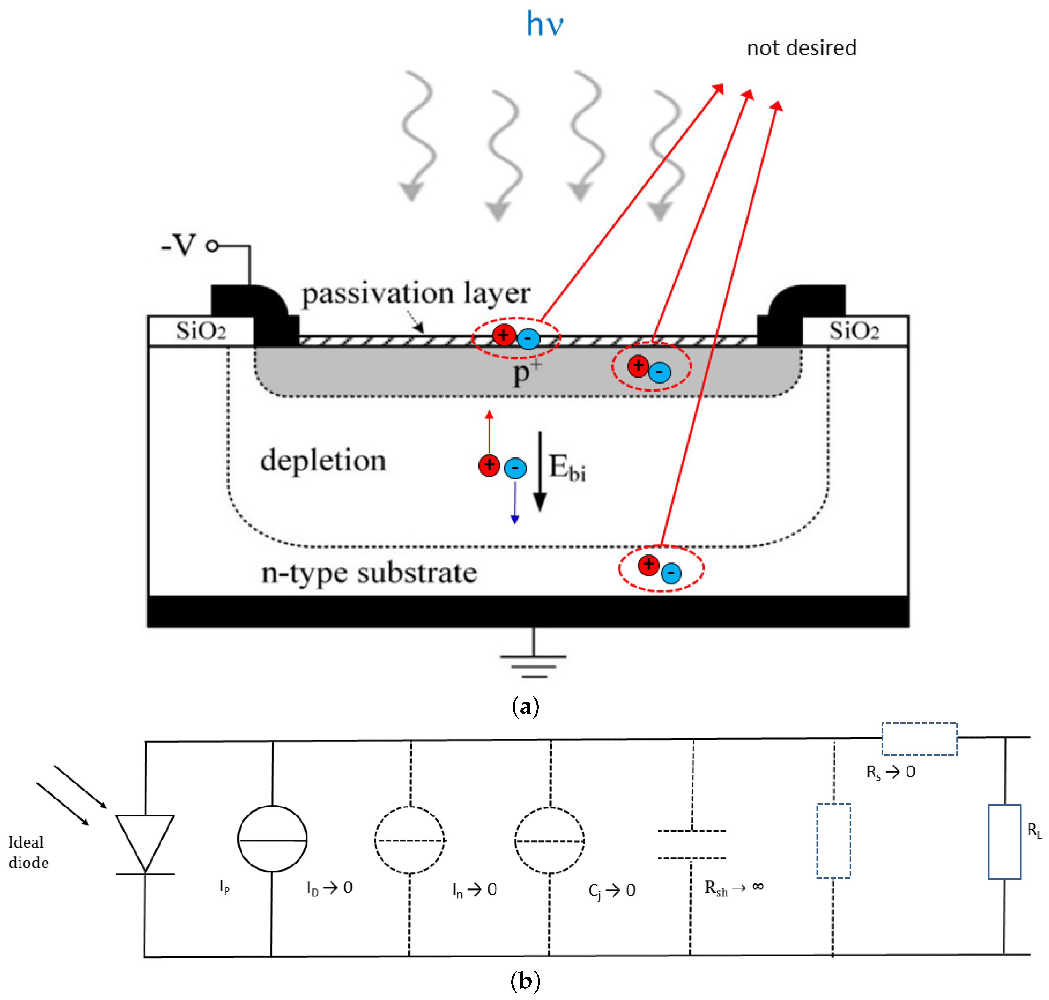
In the Introduction we revealed the main application driving the development of the PureB process: the detection of low-penetration depth radiation such as UV photons and low-energy electrons. Here we shall present the most attractive characteristics of the boron-silicon junction, in its application as a photodetector (photodiode). For this purpose we shall use as a reference the characteristics of an ideal photodetector, as presented in Table 1 and Figure 2 [19]. Figure 2 shows the vertical cross section of a silicon p-n junction photodetector and its electric circuit equivalent. Table 1 presents the parameter values of an ideal silicon photodiode, which provide the best performance with respect to: responsivity, resolution, speed and stability.

2.2.1. Responsivity

The structure of the boron-silicon junction satisfies in an excellent way the three parameters affecting the responsivity: passivation layer thickness, depletion depth and width (see Table 1). The junction can be essentially created by a single layer of boron atoms deposited on the n-type silicon substrate, in such a way that chemical bonds are formed between the boron atoms and the surface silicon atoms.
For reliable protection of the underlying silicon from oxidation and potentially detrimental environment conditions, a few extra boron layers with a total thickness of a few nanometers are deposited in practice. The depletion region, where the photogenerated electron-hole pairs can be separated and collected, starts from the very first atomic layer of the underlying n-type silicon substrate. The lost radiation absorbed in the passivation layer is minimal due to its thinness. Figure 3 shows the measured spectral responsivity of a boron-silicon junction with a ∼5 nm amorphous boron protection layer in the extreme ultra violet (EUV) spectral range, compared with the theoretically attainable values for an ideal Si-based photodetector and a commercial n+p photodiode (SXUV from ODC) [19,20]. The measured responsivity above the silicon edge (12.4 nm) is 0.265 A/W, which is very close to that of an ideal lossless system (0.27 A/W), indicating 100% internal quantum efficiency. The slight drop in responsivity at wavelengths shorter than the silicon edge can be assigned to a very thin silicon absorbing layer above the depletion zone. However, most probably another phenomenon is playing a dominant role here: after the silicon edge, the penetration depth of the photons decreases significantly leading to the absorption of more photons close to the detector surface. The kinetic energy of the freed electrons is high enough to allow them to overcome the internal electric field and to move in an arbitrary direction, with some being lost due to recombination with the holes, while others may even escape from the surface of the detector as secondary electrons.
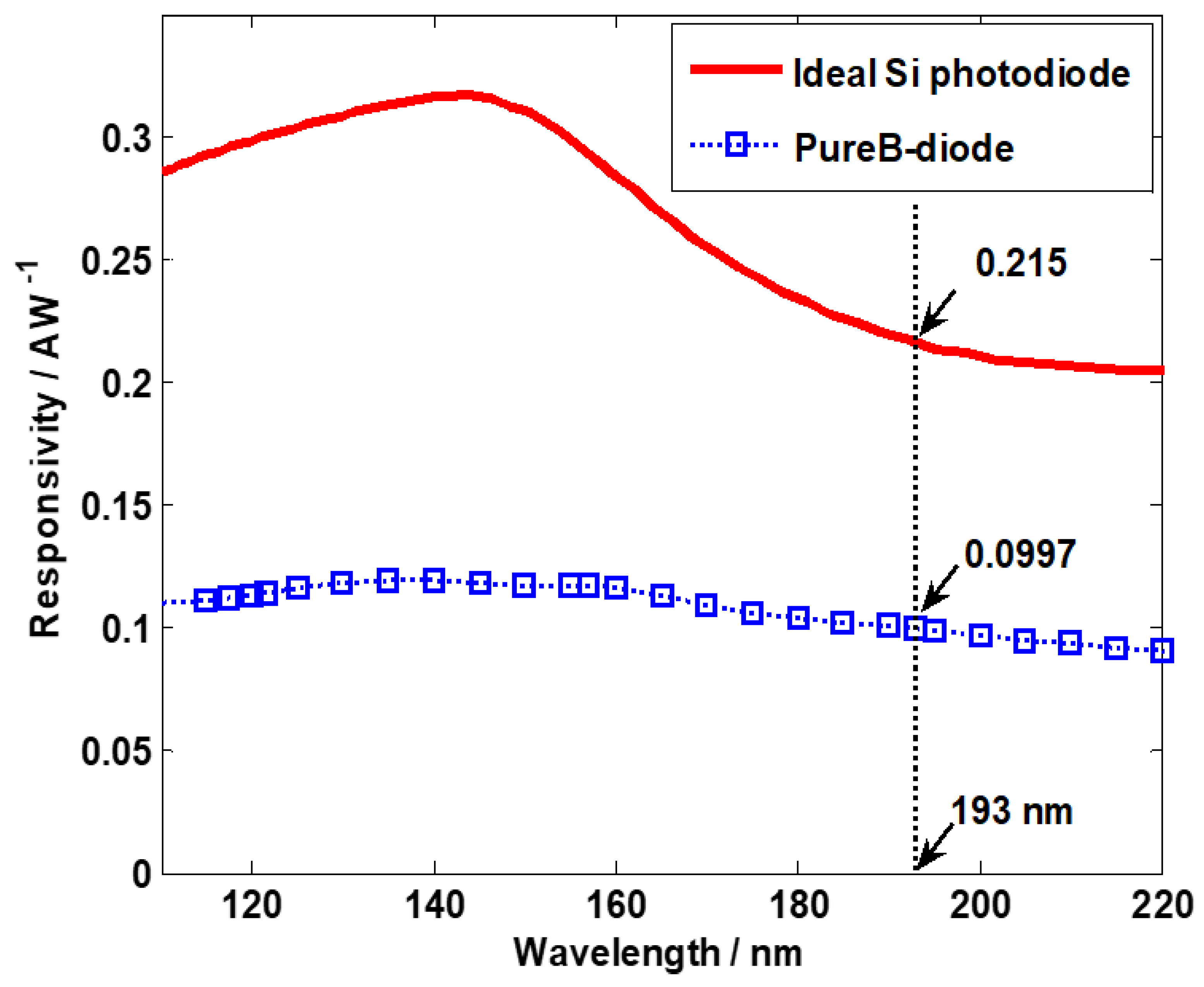
Figure 4 shows the measured spectral responsivity of a boron-silicon photodiode in the deep ultra violet (DUV) and vacuum ultra violet (VUV) spectral ranges [19]. As indicated in the figure, based on the measured responsivity at a 193 nm wavelength (0.0997 A/W) and the theoretical value (0.215 A/W), the quantum efficiency is: Q E = 0.0997 / 0.215 0.46 . Considering the nearly 100% quantum efficiency measured at a 13.5 nm wavelength (Figure 4), the loss due to the photon-generated electron-hole pairs recombining in the diode depletion region can be regarded as negligible. The main reason for the quantum efficiency drop in the VUV/DUV spectral range, besides the reflection-induced photon loss on the diode surface, is the extremely low penetration depth of the photons in the boron and silicon: only a few nanometers [21]. Because of this, even a 2-nm-thick boron layer will absorb a substantial part of the incident radiation.

2.2.2. Resolution

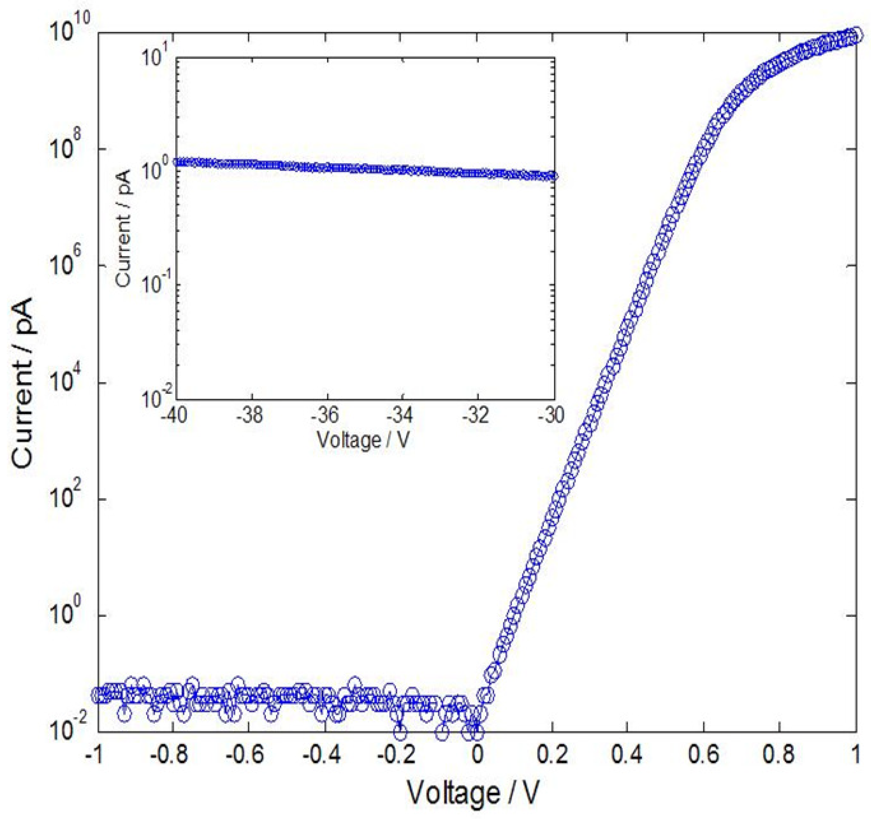
For achieving a very high resolution it is very important the interface between the silicon substrate and the passivation layer on top of it to be defect free. This is achieved by the PureB CVD process, during which the boron atoms form strong chemical bonds with the surface silicon atoms. The number of silicon dangling bonds (acting as recombination centers is extremely small. This results in an excellent I-V characteristic typical for a high-quality deep p-n junction, with a very low reverse-bias (dark) current and an ideality factor very close to 1 (Figure 5) [22], despite the fact the depletion region starts literally from the boron-silicon interface. A low dark current means a very low shot noise associated with it. The low value of the dark current maintained at high reverse-bias voltage is an evidence for a very high shunt resistance Rsh.

2.2.3. Stability

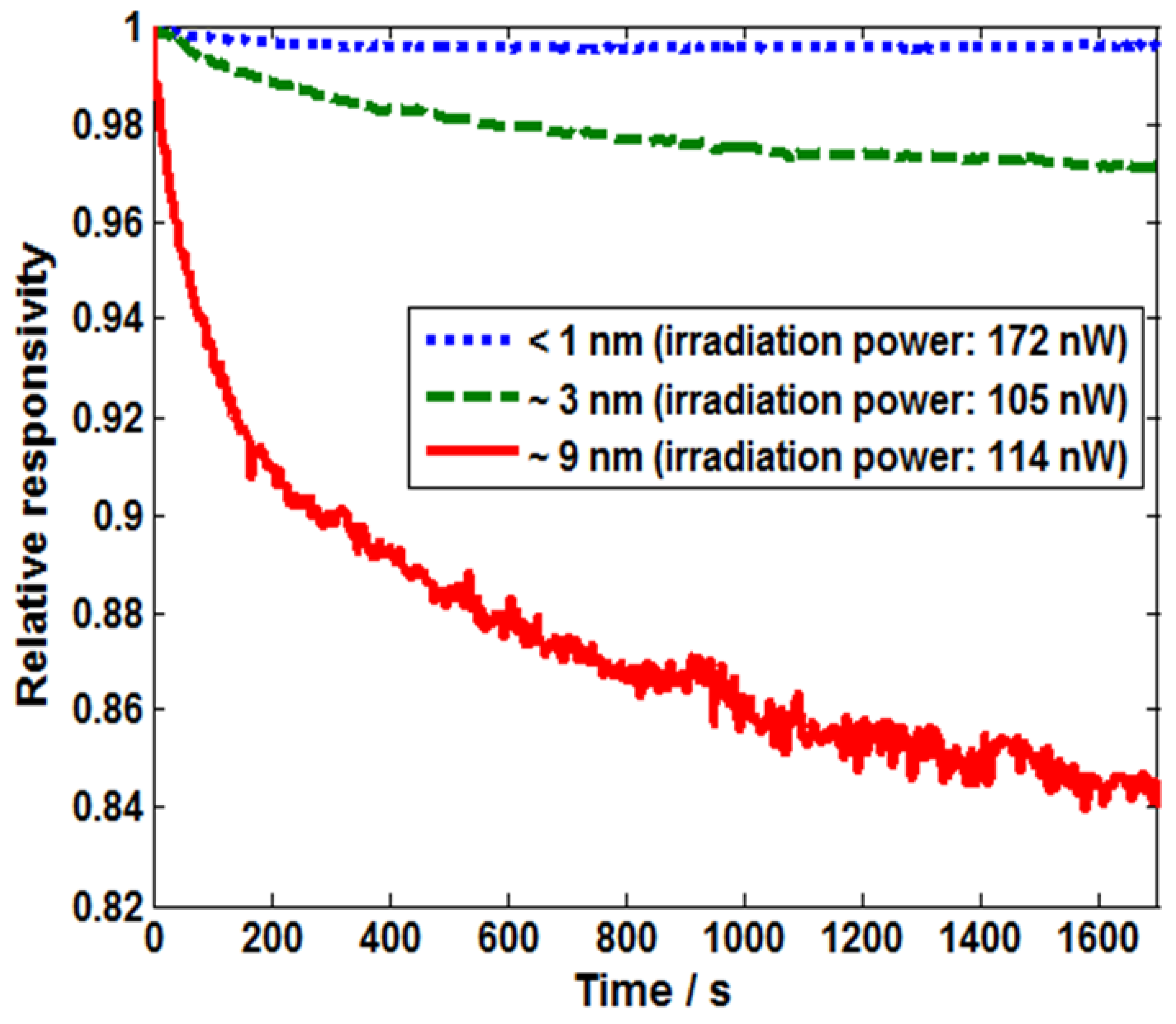
The strong chemical bonds formed between the silicon and the boron atoms provide an excellent radiation shield, as they cannot be destroyed by UV photons or low-energy electrons. Experiments with extensive exposure up to 220 kJ/cm2 of a boron-silicon photodiode at 13.5 nm radiation could not reveal a measurable degradation of the responsivity [23]. A very small amount of responsivity degradation was observed in the VUV spectrum. Figure 6 shows the responsivity degradation of three boron-silicon junctions exposed to 121 nm radiation (radiation around 120 nm wavelength is considered the most challenging in the VUV spectrum) [19]. The difference between the three samples is the oxygen content on the surface, expressed as a thickness in nanometers. In this experiment high exposure levels are not necessary, as any available drop in responsivity is evident almost immediately at the start of the VUV exposure, subsequently settling to its lower level. The presence of oxygen is assigned to local oxidation of silicon through pin holes in the thin boron layer which only partially covers silicon. With VUV exposure the oxidized silicon surface is positively charged due to the secondary electron emission, temporarily reducing the responsivity. As can be seen in Figure 6, with 1 nm oxide the degradation is extremely small—within the margin of uncertainty of the measurement equipment. It is important to mention that this kind of degradation is recoverable with time as the positive charge dissipates very slowly.
Another factor influencing the photodiode stability is the working environment. In this aspect, the boron-silicon junction demonstrates very high robustness to harsh working conditions. Boron itself is a very stable material at room temperature. Furthermore, a nanometer-thin amorphous boron layer, when completely covering the underlying silicon, acts as an excellent barrier protecting the silicon substrate from detrimental environmental elements such as hydrogen radicals and oxygen plasma, used for surface cleaning purposes. Extensive exposure to such elements has not resulted in noticeable deterioration of the electrical or optical characteristics of the boron-silicon photodiode [23].

2.2.4. Operational Speed

For a fast reaction to pulsed radiation, the photogenerated charge must be removed quickly from the depletion region of the photodetector and delivered to the interface electronics. For this purpose the time constant of the detector—defined by the junction capacitance Cj and the series resistance Rs—must be small (Figure 2b). The value of the series resistance is dominated by the sheet resistance of the surface of the detector. This is because after separation, the photogenerated charge must reach the top ring electrode (Figure 2a) by moving along the surface of the detector. However, due to the high resistivity of the very thin boron layer and the fact that the depletion region starts from the silicon surface, the sheet resistance is very high. This makes the boron-silicon photodiode extremely slow. Furthermore, unlike a typical p-n junction detector—where the time constant can be decreased by reducing Cj with the application of a higher reverse-bias voltage, the same approach does not work well with the boron-silicon detector. Just the opposite, the time constant of the boron-silicon detector increases with a higher reverse-bias voltage despite the reduction in the junction capacitance. This is because apparently the series resistance increases faster than the decrease in the capacitance [24].
A solution to this problem is to trade some responsivity for the benefit of the time constant. For example, deploying a metal Al grid on top of the boron layer, which covers just 1% of the surface, leads to a dramatic reduction in the sheet resistance and the time constant, respectively [19].

3. Boron-Silicon Junction Formation Premise Based on ab Initio Modeling

To gain insight into the preparation processes and the structural and electronic properties of the boron-silicon heterojunction, we modeled the decomposition of B2H6 molecules and the deposition of BHn (n = 1–4) molecular/radicals on a Si substrate at the early stages of the PureB processes [10,25,26], and a-B/c-Si interfaces [10,27]. Here we briefly review our recent theoretical work on the local structure, chemistry and electronic properties of a-B/c-Si interfaces. At present, Si{0 0 1} wafers are used to prepare boron-silicon heterojunctions. The unusual structure of the Si{1 1 1} surfaces and commercial availability of Si{1 1 1} wafers stimulate us to include a-B/Si{1 1 1} interfaces in our study, as well.
Supercells were built for ab initio molecular dynamics simulations. A tetragonal supercell with a = 3 a 0 = 16.45 Å ( a 0 is the lattice parameter of cubic Si at the simulation temperature), c = 19.18 Å for a-B/Si{0 0 1}. This cell contains 444 atoms (144 c-Si and 300 a-B). For a-B/Si{1 1 1}, we built a hexagonal cell with a = 2 2 a 0 = 15.15 Å, c = 26.65 Å, which contains 492 atoms (192 Si and 300 B). These large supercells are required in order to prevent the interaction between the two surfaces and eliminate the risk of the a-B artificial crystallization.
All simulations were performed using the first-principles code VASP (Vienna Ab initio Simulation Package). This code is based on a pseudo-potential plane-wave approach within the density-functional theory (DFT) [28]. It employs the projector augmented-wave (PAW) method [29], and it allows variable fractional occupation number, which works well for interfaces between insulators and metals [28,30]. An ab initio molecular dynamics (AIMD) simulation employs the finite-temperature density-functional theory of the one-electron states, where the exact energy minimization and calculation of the exact Hellmann-Feynman forces occur after each MD step using both the preconditioned conjugate techniques, and the Nose dynamics to generate a canonical NVT ensemble [28]. The exchange and correlation terms are described using the generalized gradient approximation (GGA-PBE) [31]. For electronic structure calculations, we used cut-off energies of 400.0 eV for the wave functions, 550.0 eV for the augmentation functions, and dense grids in the irreducible Brillouin zone (BZ) of the cells [32]. For the AIMD simulations we used cut-off energies of 250.0 eV and the Γ -point in the BZs. This is due to the whole system lacking periodicity in such crystal/amorphous interfaces [28,33].
We created amorphous B by first equilibrating the samples at 3000 K for 2000 iterations (at 1.5 fs per iteration, which totals 3 ps) and then cooling systems to the desired temperature. Next the obtained a-B samples were placed on the crystalline Si substrates (c-Si), forming a-B/c-Si interfaces for the subsequent AIMD simulations. The prepared a-B/c-Si systems were then allowed to equilibrate at 1000 K with the Si atoms in the substrate pinned. Then, all the atoms including the substrate were allowed to relax at 1000 K over a period of 6 ps. Finally we relaxed the atoms at 0 K to eliminate internal forces and stress.

3.1. Local Chemistry of the c-Si/a-B Interfaces

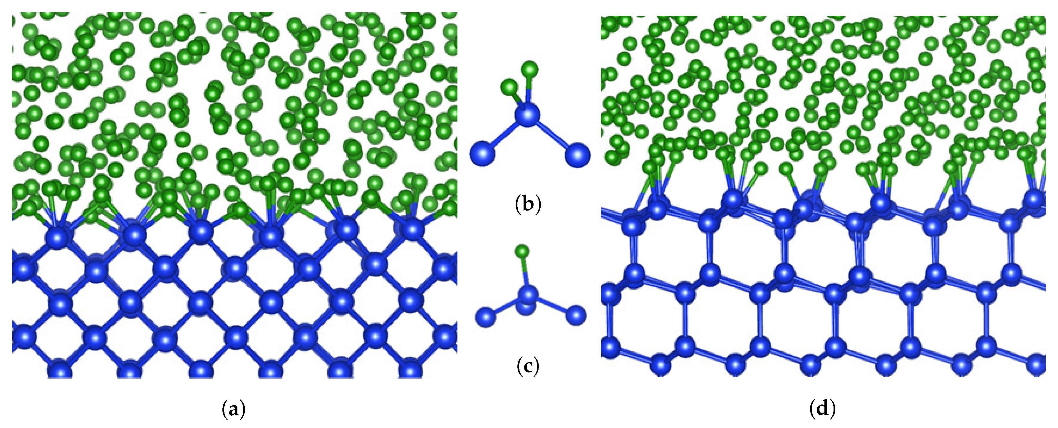
Figure 7 displays snapshots of the relaxed a-B/Si{0 0 1} and a-B/Si{1 1 1} interfaces from the AIMD simulations with the inputs, settings and treatments presented in the previous section. From Figure 7 we find the following features common to both interfaces:
  • The Si atoms in the substrates are positioned in an orderly fashion, whereas the B atoms remain disordered;
  • There is a spacing separating the crystalline Si and amorphous B at both the Si{0 0 1}/a-B (Figure 7a) and the Si{1 1 1}/a-B (Figure 7d) interfaces;
  • There is a certain amount of disordering for the surficial Si atoms at both substrates.
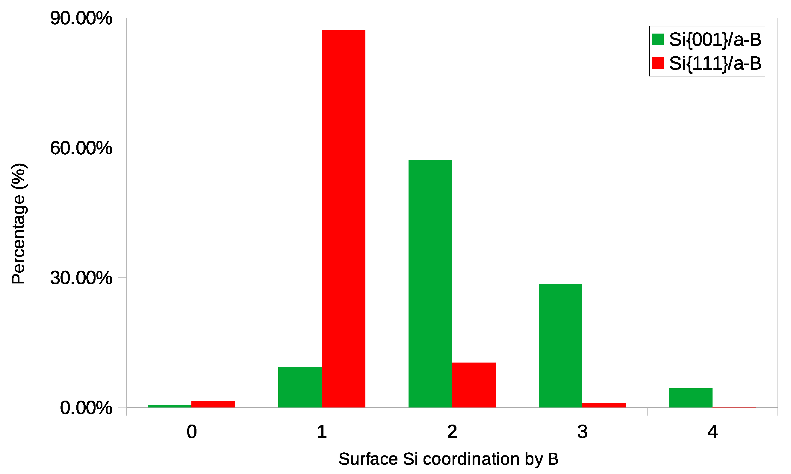
A closer look reveals subtle differences between the two interfaces. The spacing between the c-Si substrate and a-B at a-B/Si{1 1 1} is apparently larger than that at a-B/Si{0 0 1}. Moreover, the surficial Si atoms at a-B/Si{0 0 1} have more B neighbors than those at a-B/Si{1 1 1}. We analyzed the Si-B bonding at both interfaces with about 20 nterfaces each. The cut-off of the Si-B bonds is 2.28 Å, which is 10 % longer than the average value of the B-B bond (1.79 Å) and the Si-Si bond-length (2.35 Å) in the elemental solids, respectively, taking into account the exponential decay of bond strength as a function of interatomic distance [34]. The results are plotted in Figure 8.
As shown in Figure 8, most surficial Si (88%) at the a-B/Si{1 1 1} interfaces have only one B neighbor. Another 10% of the interfacial Si atoms are coordinated with two B atoms. The Si coordination of the surficial Si atoms at the a-B/Si{0 0 1} interfaces is more complex. The surficial Si atoms with two B neighbors are dominant at the a-B/Si{0 0 1} interface (57%). 29% of the interfacial Si atoms have three B neighbors, a relatively small amount of the interfacial Si (9%) have one B neighbor, and only 4% of the surface Si atoms have four B neighbors. The larger variety of Si coordination at the a-B/Si{0 0 1} interfaces is related to the reduced symmetry constraint from the Si substrates, as each superficial Si is bonded to only two Si atoms at the subsurface. The different local Si-B bonding indicates variation in the B arrangements at the interfaces. The dominant surficial Si atoms with one B and three Si atoms at a-B/Si{1 1 1}, and those Si with two B neighbors and two Si neighbors at a-B/Si{0 0 1}, satisfy the sp3 type hybridization for Si [35].
The statistical analysis also produced the averaged spacing between surficial Si and the neighboring B atoms. A larger spacing (2.0 Å) was obtained at the a-B/Si{1 1 1} interface compared to that at the a-B/Si{0 0 1} interface (1.2 Å).

3.2. Electronic Properties of the c-Si/a-B Interfaces

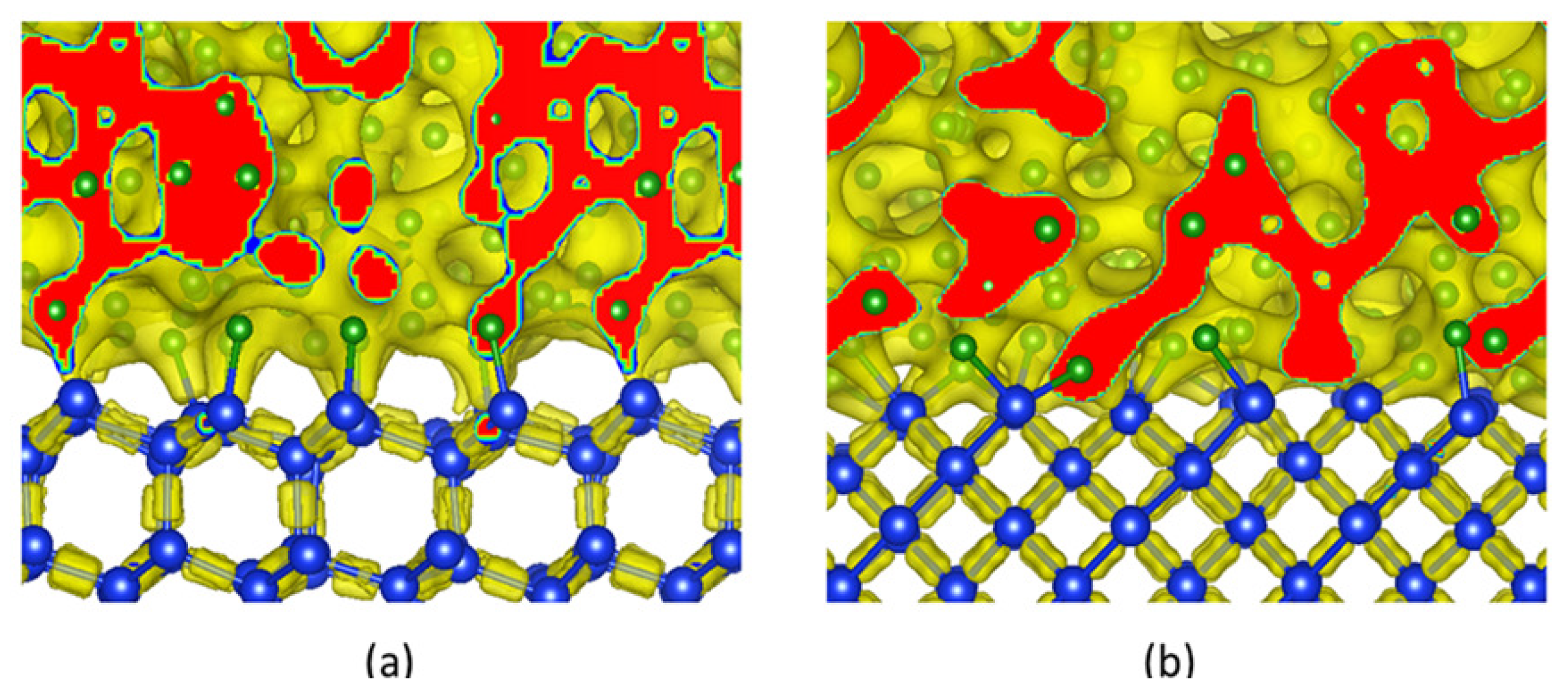
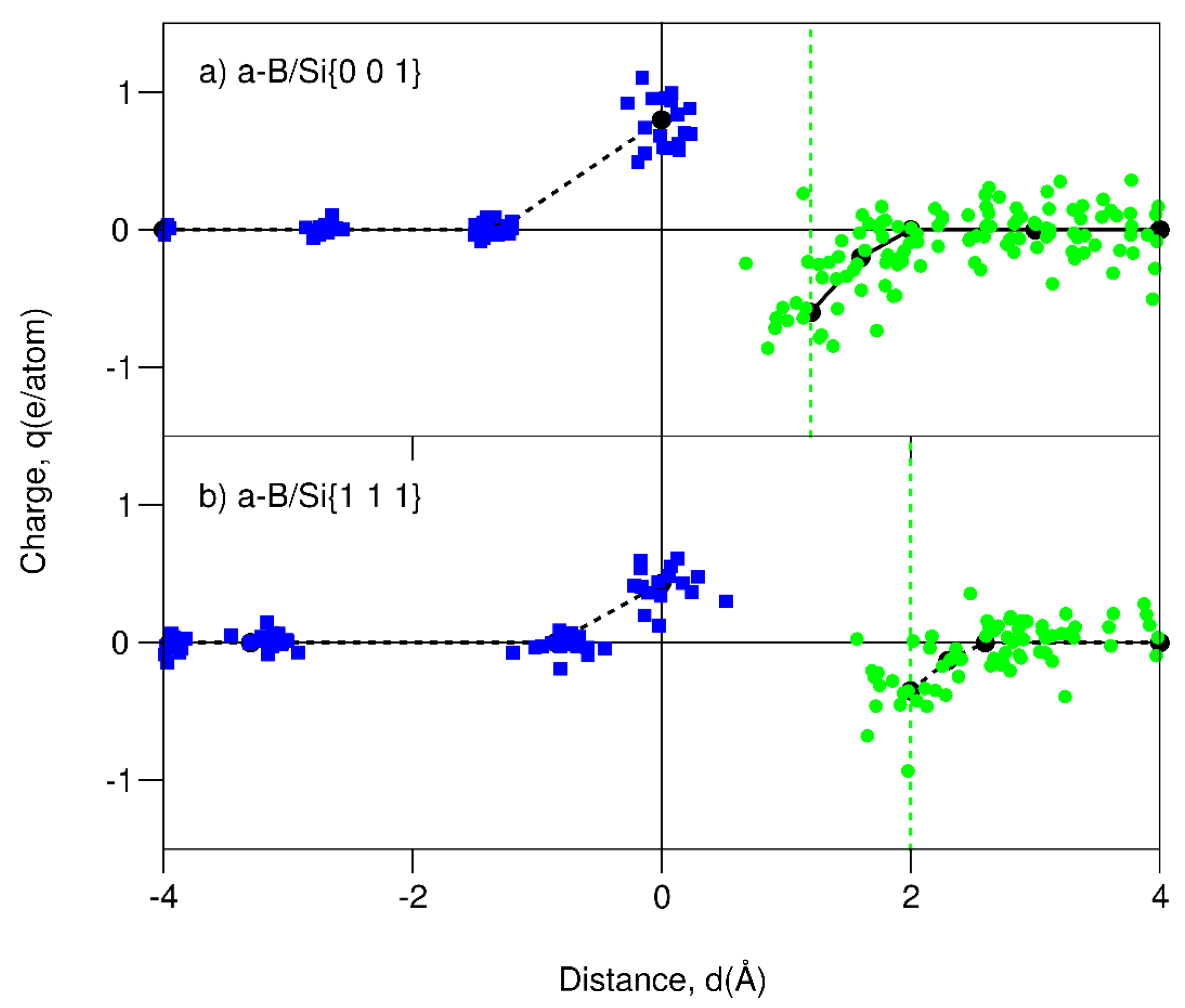
Electronic structure calculations were performed for the relaxed interfaces. Fractions of the obtained electron density distributions are shown in Figure 9. Based on the electron densities in the interface systems, we analyzed the charges at each atomic site using the Bader charge model [36]. The charges obtained at the atomic sites at both interfaces are plotted in Figure 10.
As shown in Figure 9, the electron clouds form regular shapes and are concentrated around the Si-Si bonds in the substrates. This corresponds to the crystalline structures and their covalent nature. Meanwhile, electron clouds in the a-B part show irregular forms of high electron density, which corresponds to the local disordering. At the interfacial region, there are clear clouds for both interfaces between the interfacing Si-B atoms, which indicate chemical bonding. Figure 9 also shows that the electron clouds are more present at the B atoms, which is an indication of charge transfer from the Si atoms to the B atoms. At the a-B/Si{1 1 1} interface, each surficial Si is coordinated to one B with the electron clouds forming regular shapes, whereas at a-B/Si{0 0 1}, each Si has two or three B neighbors with dense electron clouds (see Figure 9 for both).
Figure 10 includes the charges at the atomic sites at both interfaces. Clearly, the Si and a-B atoms located away from the interfacial layers are electronically neutral. Charge transfer only occurs from interfacial Si atoms to interfacial B atoms. Analysis results revealed an average amount of charge transfer of 0.75 e/Si ( 4.7 × 10 18 e/m2) at a-B/Si{0 0 1}, and 0.40 e/Si ( 2.7 × 10 18 e/m2) at a-B/Si{1 1 1}. These values correspond to the number of Si-B bonds at the interfaces. These values are smaller than those from the ionic model (Si2+ at a-B/Si{0 0 1} and Si+ at a-B/Si{1 1 1}). This is indicative of a bond of a strong covalent nature between the interfacing Si and B atoms (electronegativity value is 2.04 on Pauling scale for B and 1.90 for Si).
The charge transfer from the interfacial Si to B induces charge barriers at the a-B/c-Si interfaces. The formation of the charge barriers is essential for the heterojunctions/diodes. It also causes band bending of the heterojunctions.

3.3. Band Bending for the Electronegativity Junctions

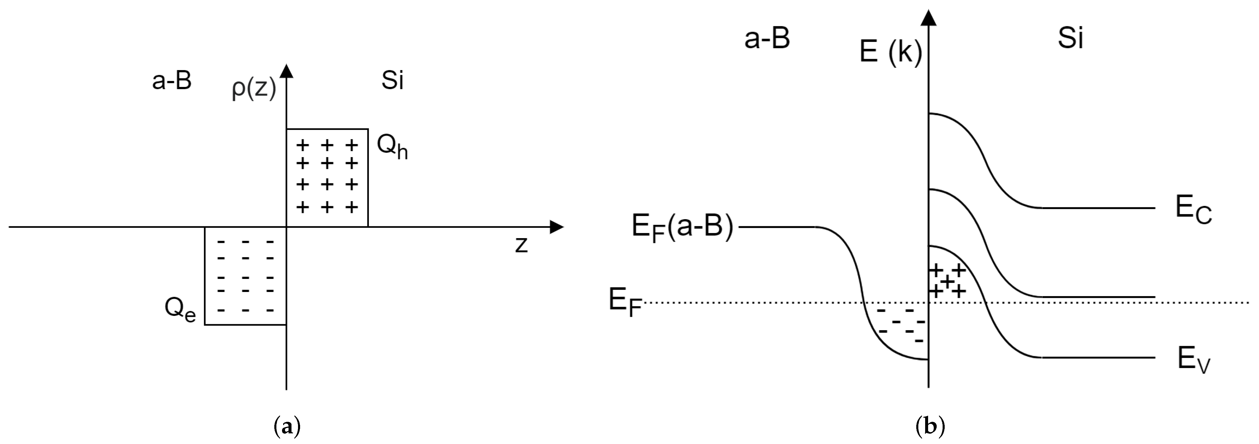
Our AIMD simulations and electronic structure calculations for the a-B/c-Si interfaces revealed the formation of well-separated Si-B interfaces. Charge transfer occurs from the interfacial Si to B, forming Si+q/B-q polar plates. Moreover, our study also showed that amorphous B located away from the interfaces is intrinsically a ‘bad’ metal with localized defect states. Therefore, at a-B/c-Si interfaces, the Fermi level of a-B will be changed near the interface due to extra electrons from Si filling of the defect states. Based on the results above and the semiconducting nature of bulk Si, we can build a band bending model for the boron-silicon heterojunctions. Together with the charge model, it is schematically shown in Figure 11.
Figure 11a schematically represents the charge model with the Q h = 0.70 e/Si at the a-B/Si{0 0 1}, and Q h = 0.45 e/Si at a-B/Si{1 1 1} interfaces. The spacing between the positively charged Si and the negatively charged B has an averaged value of about 1.2 Å at a-B/Si{0 0 1} and 2.0 Å at a-B/Si{1 1 1}, respectively. Based on these data, we obtained charge barriers of about 11 V for a-B/Si{0 0 1} and 10 V for a-B/Si{1 1 1}. These barrier values correspond to the balance between the Si-B interaction and anisotropy of the Si surfaces.
The charge transfer and corresponding charge barriers cause band bending at the a-B/c-Si interfaces, as schematically shown in Figure 11b. The boron-silicon heterojunction properties essentially originate from the charge transfer occurring at the interfaces due to the differences between the electronegativities of Si and B.
The abundance of positive charge in the top atomic layer of the n-type silicon substrate acts as a highly doped p-region in a p-n junction, attracting free electrons from the bulk n-type silicon, and leading to the formation of a depletion region [10,27]. The significant amount of positive static charge at the surface of the silicon n-type substrate explains the high Gummel Number and the low saturation current of the boron-silicon junction, which is typical for high-quality deep p-n junctions.

4. Conclusions

Many research endeavors throughout the history of science, aside from achieving their primary research goals, have managed to generate unexpected additional new knowledge. We believe that this is also the case with the development of PureB technology. For many years the research efforts have been mainly focused on the development of the process itself. Only recently has the rectifying junction created through the PureB process—demonstrating properties not typical for a shallow p-n junction and any other existing rectifying junction—attracted more attention. In this paper we presented the main features of the PureB process and the qualities of the boron-silicon junction as a radiation detector. We also discussed how the understanding of the boron-silicon junction formation has evolved. The recently proposed quantum-mechanical junction formation mechanism presented proves the power of quantum-mechanics-based approaches to solid-state physics and materials science, offering a world of rich variety.
Overall, our understanding is that the chemical interaction between the surface atoms of crystalline silicon and the first atomic layer of the amorphous boron is the dominant factor leading to the rectifying function of boron-silicon junctions. Obviously, boron doping is not present in this model and thus the boron-silicon junction does not belong to p+n type junctions. Although a-B exhibits a high density of states in the band gap of Si, these states are of a localized nature. The electrons in a-B are conducted via a hopping mechanism, thereby disqualifying the a-B/c-Si diodes from the category of Schottky junctions. Furthermore, the a-B/c-Si diodes cannot be classified into any of the existing types of heterojunctions in semiconductor physics.
The new junction has the application potential of reaching far beyond its primary target. The new junction formation mechanism may lead to a technology breakthrough in a number of scientific fields such as: semiconductor wide-bandgap material processing, electron microscopy, optics, space exploration, chemical engineering, quantum mechanics, nano-materials, etc. Furthermore, this type of junction may trigger many innovations in industry, e.g., direct ultraviolet detection and imaging, energy harvesting (solar cells), etc.
New possible research directions may include: (i) better understanding of the quantum phenomena responsible for the formation of the boron-silicon junction; (ii) creation of an analytical model for the boron-silicon junction and extending this model to other semiconductor materials, such as SiC and wide-bandgap materials; and (iii) study of the electrical, optical and mechanical properties of devices developed for different applications, based on the boron-silicon junction technology.

Author Contributions

S.N.: writing Section 1 and Section 2.2, contributing to Conclusions; P.S.: writing Section 2.1; C.F. and P.X.F.: writing Section 3, contributing to Conclusions. All authors have read and agreed to the published version of the manuscript.

Funding

This research received no external funding.

Conflicts of Interest

The authors declare no conflict of interest.

References

  1. Sarubbi, F.; Nanver, L.K.; Scholtes, T.L. CVD Delta-Doped Boron Surface Layers for Ultra-Shallow Junction Formation. ECS Trans. 2006, 3, 35–44. [Google Scholar] [CrossRef] [Green Version]
  2. Nanver, L.K.; Sarubbi, F.; Gonda, V.; Popadic, M.; Scholtes, T.L.; de Boer, W.; Buisman, K. Extremely ultrashallow junctions for a high-linearity silicon-on-glass RF varactor-diode technology. Extended Abstracts. In Proceedings of the 2008 8th International Workshop on Junction Technology (IWJT ‘08), Shanghai, China, 15–16 May 2008. [Google Scholar] [CrossRef]
  3. Sarubbi, F. Characterization of Pure Boron Depositions Integrated in Silicon Diodes for Nanometer-Deep Junction Applications. Ph.D. Thesis, TU Delft Repository, Delft, The Netherlands, 2010. [Google Scholar]
  4. Sarubbi, F.; Nanver, L.K.; Scholters, L.M. High Effective Gummel Number of CVD Boron Layers in Ultrashallow p+n Diode Configurations. IEEE Trans. Electron. Devices 2010, 57, 1269–1278. [Google Scholar] [CrossRef]
  5. Nanver, L.K.; Qi, L.; Mohammadi, V.; Mok, K.R.M.; de Boer, W.B.; Golshani, N.; Sammak, A.; Scholtes, T.L.M.; Gottwald, A.; Kroth, U.; et al. Robust UV/VUV/EUV PureB Photodiode Detector Technology With High CMOS Compatibility. IEEE J. Sel. Top. Quantum Electron. 2014, 20, 306–316. [Google Scholar] [CrossRef]
  6. Nanver, L.K.; Sammak, A.; Mohammadi, V.; Mok, K.R.C.; Qi, L.; Sakic, A.; Golshani, N.; Derakhshandeh, J.; Scholtes, T.M.L.; de Boer, W.B. (Invited) Pure Dopant Deposition of B and Ga for Ultrashallow Junctions in Si-based Devices. ECS Trans. 2012, 49, 25–33. [Google Scholar] [CrossRef] [Green Version]
  7. Mohammadi, V.; Nihtianov, S. Low-Temperature PureB CVD Technology for CMOS Compatible Photodetectors. Ph.D. Thesis, TU Delft Repository, Delft, The Netherlands, 2016. [Google Scholar] [CrossRef] [Green Version]
  8. Knežević, T.; Suligoj, T.; Šakić, A.; Nanver, L.K. Modelling of electrical characteristics of ultrashallow pure amorphous boron p+n junctions. In Proceedings of the 35th International Convention MIPRO, Opatija, Croatia, 21–25 May 2012; pp. 36–41. [Google Scholar]
  9. Qi, L. Interface Properties of Group-III-Element Deposited-Layers Integrated in High-Sensitivity Si Photodiodes. Ph.D Thesis, TU Delft Repository, Delft, The Netherlands, 2016. [Google Scholar] [CrossRef]
  10. Mohammadi, V.; Nihtianov, S.; Fang, C. A doping-less junction-formation mechanism between n-silicon and an atomically thin boron layer. Sci. Rep. 2017, 7. [Google Scholar] [CrossRef] [Green Version]
  11. Elsayed, A.; Schulze, J. Characterization of thin Boron layers grown on Silicon utilizing molecular beam epitaxy for ultra-shallow pn-junctions. In Proceedings of the 2018 41st International Convention on Information and Communication Technology, Electronics and Microelectronics (MIPRO), Opatija, Croatia, 21–25 May 2018. [Google Scholar] [CrossRef]
  12. Thammaiah, S.D.; Hansen, J.L.; Nanver, L.K. Nanometer-Thin Pure B Layers Grown by MBE as Metal Diffusion Barrier on GaN Diodes. In Proceedings of the 2019 China Semiconductor Technology International Conference, (CSTIC), Shanghai, China, 17–18 March 2019. [Google Scholar] [CrossRef]
  13. McKernan, M.A. Magnetron sputter deposition of boron and boron carbide. Surf. Coat. Technol. 1991, 49, 411–415. [Google Scholar] [CrossRef]
  14. Mappes, G.W.; Fridmann, S.A.; Fehlner, T.P. Absolute rate of association of borane molecules. J. Phys. Chem. 1970, 74, 3307–3316. [Google Scholar] [CrossRef]
  15. Mohammadi, V.; de Boer, W.B.; Nanver, L.K. Temperature dependence of chemical-vapor deposition of pure boron layers from diborane. Appl. Phys. Lett. 2012, 101, 111906. [Google Scholar] [CrossRef] [Green Version]
  16. Sarubbi, F.; Scholtes, T.L.M.; Nanver, L.K. Chemical Vapor Deposition of α-Boron Layers on Silicon for Controlled Nanometer-Deep p+n Junction Formation. J. Electron. Mater. 2009, 39, 162–173. [Google Scholar] [CrossRef] [Green Version]
  17. Saitoh, N.; Akamine, T.; Aoki, K.; Kojima, Y. Composition and Growth Mechanisms of a Boron Layer Formed Using the Molecular Layer Doping Process. Jpn. J. Appl. Phys. 1993, 32, 4404–4407. [Google Scholar] [CrossRef]
  18. Mohammadi, V.; Nihtianov, S. Low temperature, 400 °C, pure boron deposition: A solution for integration of high-performance Si photodetectors and CMOS circuits. In Proceedings of the 2015 IEEE SENSORS, Busan, Korea, 1–4 November 2015. [Google Scholar] [CrossRef]
  19. Shi, L. Performance Analysis of Si-Based Ultra-Shallow Junction Photodiodes for UV Radiation Detection. PhD Thesis, TU Delft Repository, Delft, The Netherlands, 2013. [Google Scholar] [CrossRef]
  20. Shi, L.; Sarubbi, F.; Nihtianov, S.N.; Nanver, L.K.; Scholtes, T.L.M.; Scholze, F. High performance silicon-based extreme ultraviolet (EUV) radiation detector for industrial application. In Proceedings of the 2009 35th Annual Conference of IEEE Industrial Electronics, Porto, Portugal, 3–5 November 2009. [Google Scholar] [CrossRef]
  21. Henke, B.; Gullikson, E.; Davis, J. X-ray Interactions: Photoabsorption, Scattering, Transmission, and Reflection at E = 50–30,000 eV, Z = 1–92. At. Data Nucl. Data Tables 1993, 54, 181–342. [Google Scholar] [CrossRef] [Green Version]
  22. Shi, L.; Nihtianov, S.; Haspeslagh, L.; Scholze, F.; Gottwald, A.; Nanver, L.K. Surface-Charge-Collection-Enhanced High-Sensitivity High-Stability Silicon Photodiodes for DUV and VUV Spectral Ranges. IEEE Trans. Electron Devices 2012, 59, 2888–2894. [Google Scholar] [CrossRef]
  23. Shi, L.; Nihtianov, S.; Nanver, L.K.; Scholze, F. Stability Characterization of High-Sensitivity Silicon-Based EUV Photodiodes in a Detrimental Environment. IEEE Sens. J. 2013, 13, 1699–1707. [Google Scholar] [CrossRef]
  24. Nojdelov, R.; Nihtianov, S. Response Time of Detectors Based on a Boron-Silicon Junction. In Proceedings of the 2018 IEEE SENSORS, New Delhi, India, 28–31 October 2018. [Google Scholar] [CrossRef]
  25. Fang, C.M.; Mohammadi, V.; Nihtianov, S.; Sluiter, M.H.F. Stability, local structure and electronic properties of borane radicals on the Si(100) 2×1:H surface: A first-principles study. Comput. Mater. Sci. 2017, 140, 253–260. [Google Scholar] [CrossRef] [Green Version]
  26. Fang, C.M.; Mohammodi, V.; Nihtianov, S.; Sluiter, M.H.F. Stability, geometry and electronic properties of BH n (n = 0 to 3) radicals on the Si{001}3×1:H surface from first-principles. J. Phys. Condens. Matter 2020, 32, 235201. [Google Scholar] [CrossRef] [PubMed]
  27. Fang, P.X.; Nihtianov, S.; Sberna, P.; Fang, C.M. Interfaces between Crystalline Siand Amorphous Boron: Interfacial Chemistry and Charge Barriers. Phys. Rev. B. accepted for publication.
  28. Kresse, G.; Furthmüller, J. Efficiency of ab-initio total energy calculations for metals and semiconductors using a plane-wave basis set. Comput. Mater. Sci. 1996, 6, 15–50. [Google Scholar] [CrossRef]
  29. Blöchl, P.E. Projector augmented-wave method. Phys. Rev. B 1994, 50, 17953–17979. [Google Scholar] [CrossRef] [Green Version]
  30. Hintzsche, L.E.; Fang, C.M.; Marsman, M.; Jordan, G.; Lamers, M.W.P.E.; Weeber, A.W.; Kresse, G. Defects and defect healing in amorphous Si3N4-xHy: Anab initiodensity functional theory study. Phys. Rev. B 2013, 88. [Google Scholar] [CrossRef]
  31. Perdew, J.P.; Burke, K.; Ernzerhof, M. Generalized Gradient Approximation Made Simple. Phys. Rev. Lett. 1996, 77, 3865–3868. [Google Scholar] [CrossRef] [Green Version]
  32. Monkhorst, H.J.; Pack, J.D. Special points for Brillouin-zone integrations. Phys. Rev. B 1976, 13, 5188–5192. [Google Scholar] [CrossRef]
  33. Pasquarello, A.; Hybertsen, M.S.; Car, R. Interface structure between silicon and its oxide by first-principles molecular dynamics. Nature 1998, 396, 58–60. [Google Scholar] [CrossRef]
  34. Brown, I.D. Recent Developments in the Methods and Applications of the Bond Valence Model. Chem. Rev. 2009, 109, 6858–6919. [Google Scholar] [CrossRef] [PubMed] [Green Version]
  35. Pauling, L. The Nature of the Chemical Bond; Cornell University Press: New York, NY, USA, 1960; pp. 111–120. [Google Scholar]
  36. Bader, R.F.W. A Bond Path: A universal Indicator of Bonded Interactions. J. Phys. Chem. A 1998, 102, 7314–7323. [Google Scholar] [CrossRef]
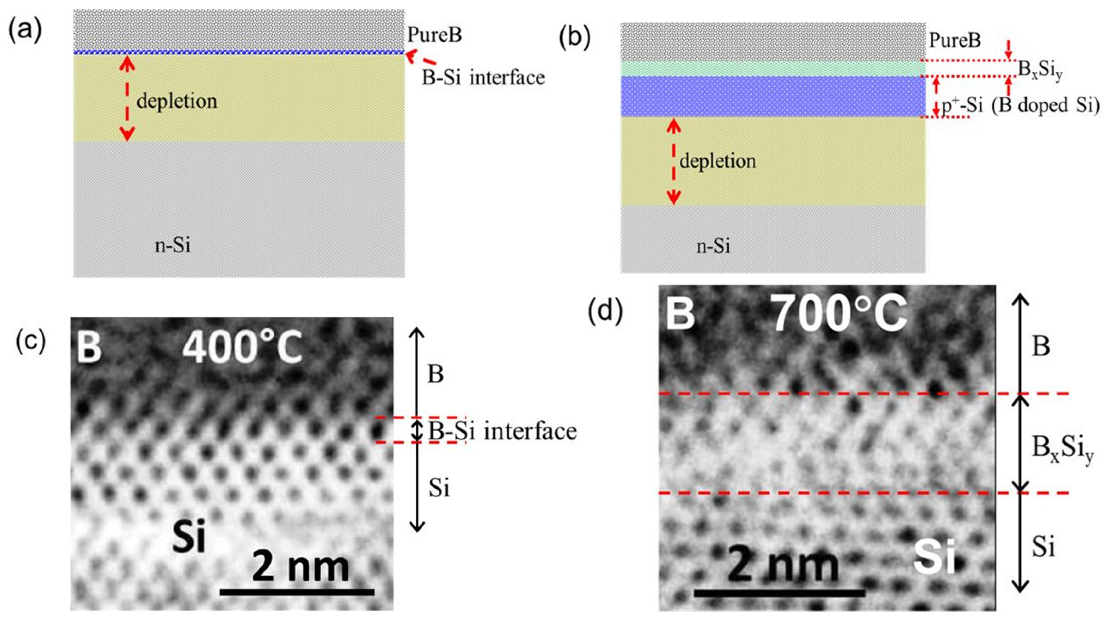
Figure 1. Schematic illustrations and High-Resolution Tunneling Electron Microscope (HRTEM) images of the cross-section of the layer stack: (a) schematic illustration of the cross-section of the B-Si junction processed at 400 °C; (b) Schematic illustration of the cross-section of the B-Si junction processed at 700 °C; (c) HRTEM image of the cross-section of the B-Si junction processed at 400 °C; (d) HRTEM image of the cross-section of the B-Si junction processed at 700 °C [10].
Crystals 11 00108 g001
Figure 2. Vertical cross section (a), and electrical equivalent circuit (b) of a silicon p-n junction photodetector, where ID is the dark current, Ip is the photogenerated current, In is the shot noise associated with the dark current, Cj is the junction capacitance, Rsh is the shunt resistance, Rs is the series resistance and RL is the load resistance [19].
Crystals 11 00108 g002
Figure 3. Measured spectral responsivity (squares) of boron-silicon photodiode in the extreme ultra violet (EUV) spectral range, compared with a commercial n+p photodiode and the theoretically attainable values for an ideal Si-based photodetector [20].
Crystals 11 00108 g003
Figure 4. Measured responsivity of a boron-silicon photodiode with ∼2 nm boron layer, in the deep ultra violet (DUV)/vacuum ultra violet (VUV) spectral ranges, compared with the theoretically attainable values for an ideal Si-based photodetector [19].
Crystals 11 00108 g004
Figure 5. I-V characteristic of a boron-silicon diode with active area 300 × 300 μ m2. The inset shows a dark current of 1 pA with a reverse bias up to −40V, corresponding to current density: ∼11 pA per square micrometer) [22].
Crystals 11 00108 g005
Figure 6. Responsivity degradation of 3 boron-silicon photodiodes with varying parasitic oxide content on the surface, at a 121-nm wavelength. The oxide content was measured by ellipsometry and is expressed as a thickness in nanometers [19].
Crystals 11 00108 g006
Figure 7. Snapshots of (a,d) the equilibrated interface and (b,c) related typical Si coordination for the Si{0 0 1}/a-B and the Si{1 1 1}/a-B interfaces, respectively. The green spheres represent B and blue Si.
Crystals 11 00108 g007
Figure 8. Distribution of the numbers of the coordination number of the interfacial Si atoms by boron at The Si{0 0 1}/a-B (circles) and Si{1 1 1}/a-B (squares) interfaces.
Crystals 11 00108 g008
Figure 9. Electron density distribution (iso-surfaces ρ 0 ( r ) = 0.075 e/Å3) and charges at the atomic sites at the (a) Si{0 0 1}/a-B and (b) Si{1 1 1}/a-B interfaces, respectively. The blue squares represent Si sites, the blue spheres the B sites and the filled black spheres for the averaged charge values. The broken red lines represents the centre of surficial Si and the broken green lines for the centres of interfacial a-B.
Crystals 11 00108 g009
Figure 10. Charges at the a-B/c-Si interfaces. The blue squares represent charges at the Si sites and green spheres represent charges at the B sites. The solid black lines indicate the peak of the outmost Si, while the dotted green lines represent the first peak of B atoms.
Crystals 11 00108 g010
Figure 11. A schematic drawing of (a) charging and (b) band bending at the ideal Si/a-B. Charge density is 4.7 · 10 18 e/m2 at Si{0 0 1}/a-B and 2.7 · 10 18 e/m2 at Si{1 1 1}/a-B based on the first-principles calculations.
Crystals 11 00108 g011
Table 1. Main characteristics and related parameters of an ideal silicon-based photodetector.
Main CharacteristicsRelated Diode ParametersIdeal Parameter Values
ResponsivityPassivation layer thickness0
Depletion depth0
Depletion widthOptimized by the photon attenuation length
ResolutionDark current0
Shunt resistance
StabilityPassivation LayerOxide-free, high-conductivity, protective
Operational speedSeries resistance0
Junction capacitance0
Publisher’s Note: MDPI stays neutral with regard to jurisdictional claims in published maps and institutional affiliations.