Abstract
Straightforward growth of nanostructured low-bandgap materials is a key issue in mass production for electronic device applications. We report here facile nanowall growth of MoS2-MoSX using sputter deposition and investigate the electronic properties of the nanowalls. MoS2-MoSX nanowalls become gradually thicker and taller, with primarily (100)-plane growth directions, with increasing deposition time. Nanowalls combine with nearby walls when a rapid thermal annealing (RTA, 200 °C–500 °C) process is applied. All samples have conventional low-bandgap semiconductor behavior with exponential resistance increase as measurement temperature decreases. The 750 nm-thick MoS2-MoSX nanowalls have a sheet carrier mobility of up to 2 cm2·V−1·s−1 and bulk carrier concentration of ~1017–1019 cm−3 range depending on RTA temperature. Furthermore, perpendicular field-dependent magnetoresistance at 300 K shows negative magnetoresistance behavior, which displays resistance decay by applying a magnetic field (MR ratio in the −1 % range at 5 T). Interestingly, 400 °C RTA treated samples show a resistance upturn when applying an external magnetic field of more than 3 T. Our research suggests tuneability of MoS2 nanowall size and mesoscopic electronic transport properties.
1. Introduction
Transition metal dichalcogenides (TMDs), including MoS2, WS2, NbSe2, and VS2, have been intensely researched because they exhibit bandgaps ranging from 0 to 2 eV. TMDs can be metals, semimetals, semiconductors, insulators, or superconductors based on the tuning of elemental composition and/or their structural parameters, including defects [1,2,3,4]. Recently, growth of TMDs, especially MoS2, with successful wafer scale production has gained attention for electronic device applications [5,6,7,8,9,10,11,12,13,14]. Two-dimensional systems and nanostructured mass production are an important topic for high performance and functional device applications [7,11,15,16,17,18,19,20,21].
MoS2, which consists of weakly bonded S-M-S sandwiched layers, is an interesting material for electronic devices [22,23,24,25,26,27], optical sensors [10,13,18,28,29,30,31], spintronic devices [32,33,34,35], and energy storage [15,17,19]. MoS2 nanostructures are attractive due to their unique properties and structural characteristics for use in multiple applications, such as sensors, biomedical probes, optical devices, energy conversion, and storage devices. However, large-scale growth while tuning their size, shape, and composition is still a challenge and few research groups have reported large-scale nanostructure growth methods. Tao et al. and Hussain et al. reported methods for an atomic layer and a few layers of MoS2 large-area growth for application to electronic devices, respectively [6,26]. Wang et al. reported the development of a simple ‘‘bottom-up’’ method for directly grown and well-dispersed ultra-small MoS2 nanodots [7]. Sari et al. reported direct growth of MoS2 nanowalls on carbon nanofibers for supercapacitor applications [15]. Kim et al. reported a large area growth method of MoS2 nanowalls for efficient photoelectric application [31]. Additionally, Alexaki et al. illustrated a different MoSX nanocrystal production method [16]. Thus, MoS2 nanostructured large-scale growth methods need to be widely developed and improved for future device applications.
In this study, we report direct growth of MoS2 nanowalls via sputter deposition and show the possibility of tunable electronic transport through electromagnetic property analysis. The growth behavior of MoS2-MoSX nanowalls was studied by changing growth time and annealing temperature. All samples show exponentially increasing resistance depending on the annealing temperature decrease, which corresponds with conventional low bandgap semiconductor behavior. The 750 nm-thick MoS2-MoSX nanowalls have a sheet carrier mobility of up to 2 cm2·V−1·s−1 and bulk carrier concentration ranging from ~1017–1019 cm−3, depending on the annealing temperature. Moreover, perpendicular field dependent magnetoresistance at 300 K, which displays resistance decay by applying a magnetic field, shows negative magnetoresistance behavior. Interestingly, 400 °C rapid thermal annealing (RTA)-treated samples show resistance upturn when applying an external magnetic field of more than 3 T. These results show the feasibility of electromagnetic property tuning through growth conditions and post treatment, such as an annealing process.
2. Materials and Methods
2.1. MoS2 Nanowall Growth
MoS2 nanowalls were grown on soda-lime glass substrates and SiO2(400 nm)/Si wafers using a sputtering system. In our sputtering system, the distance between the substrate and the target is 95 mm. The base pressure of the sputter chamber was 8 × 10⁻⁶ mTorr. Deposition was carried out at a pressure of 10 mTorr by flowing Ar gas (25 sccm) with 100 W RF power and using a MoS2 target (99.5 % purity, 4-inch diameter, 1/8-inch thickness) with a Cu backing plate while the substrate was rotated at a speed of 5 rpm and was at room temperature. MoS2 nanowalls were grown on glass substrate or Si wafers with maximum diameters of 6 inches. For the investigation of the annealing effect, the as-grown MoS2 nanowall samples underwent an RTA (RTP600, LAT Co. Ltd., Osan-si, Korea) process for 10 min at temperatures ranging from 200 to 500 °C in a vacuum.
2.2. Characterization of the MoS2 Nanowalls
The size and thickness of the nanowalls were confirmed using field emission scanning electron microscopy (FE-SEM, Sirion 400, FEI, Waltham, MA, USA) and atomic force microscopy (AFM, DI-3100, Veeco, Plainview, NY, USA). The change in crystallinity of annealed samples was characterized using X-ray diffraction (XRD, D/MAX-2500, RIGAKU, Tokyo, Japan) and Raman spectroscopy (alpha 300R, WiTec, Ulm, Germany). All electrical measurements were performed at low pressure (below 0.01 Torr) in a PPMS (Physical Property Measurement System; Quantum Design, San Diego, CA, USA) for temperatures ranging from 100 to 300 K and with an external perpendicular magnetic field of up to 5 T. The Van der Pauw (VDP) geometry was used to connect the sample to the sample puck through copper wire bonded by Ag or paste. A Keithley 2636 source meter and Keithley 2182 nanovoltmeter were used to apply source current and to detect voltage via programmed LabVIEW software.
3. Results and Discussion
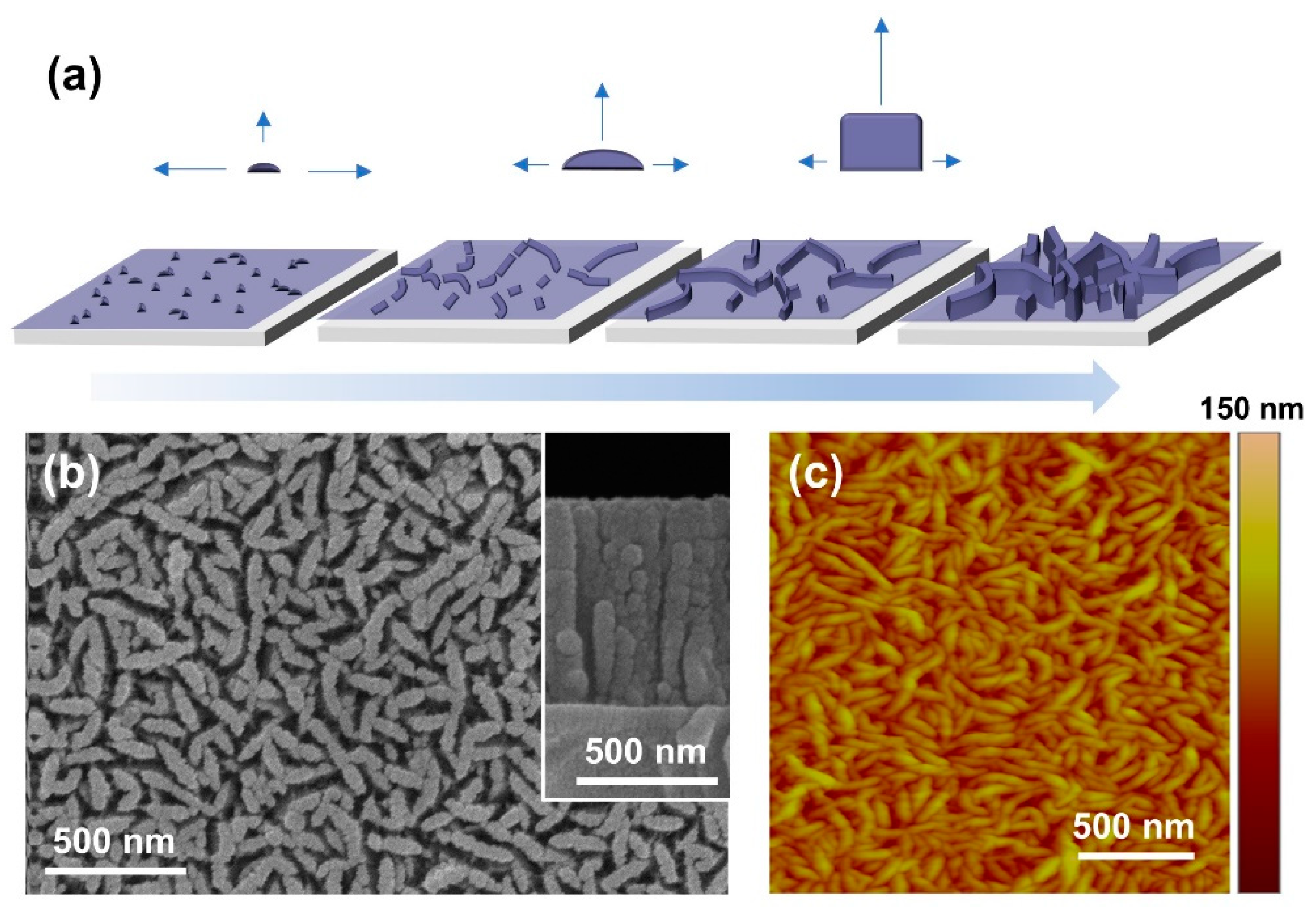
Figure 1a shows brief illustrates the MoS2-MoSX nanowall growth sequence. During sputter deposition on glass substrates, polycrystals of MoS2-MoSX formed as a thin film and nanostructured islands. Then, the nanostructured islands increase in size and height as the deposition progresses. As a result, high-density nanowalls are grown after a total sputtering deposition time of 3000 s, as shown in Figure 1. The average thickness of the MoS2-MoSX nanowalls are confirmed to be approximately 52 nm by the SEM and AFM analysis shown in Figure 1b,c (Figure 1b inset shows approximately 750 nm-tall nanowalls). In our system, nanowalls could be grown on 6-inch wafers. Supplementary Materials Figure S1 shows MoS2-MoSX nanowalls grown on a 6-inch SiO2/Si wafer with a total thickness deviation across the wafer within 10 nm.

Figure 1.
(a) Schematic illustration of the nanowall growth sequence. (b) Scanning electron microscopy (SEM) images and (c) atomic force microscopy (AFM) profile of the as-grown MoS2-MoSX nanowall surface after 3000 s of sputter deposition.
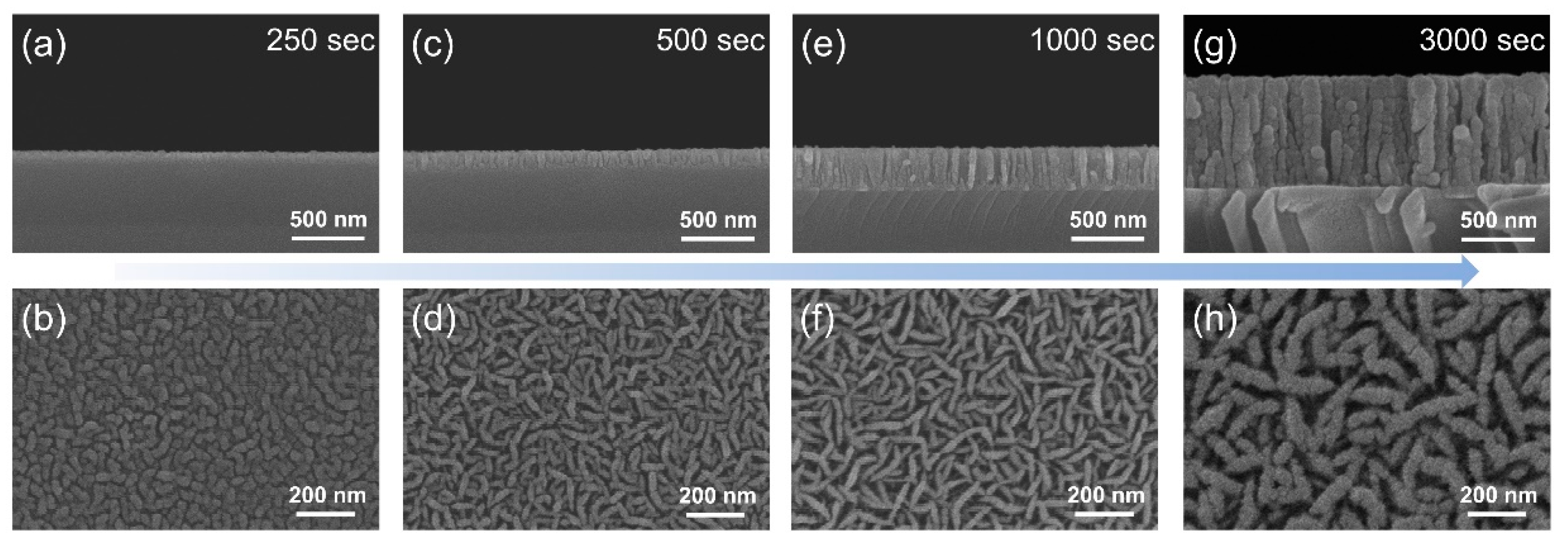
Images in Figure 2 indicate that step-by-step growth depends on deposition time. As illustrated in Figure 1a, a film with islands growing on the surface, with preferred growth direction, appears for a deposition time of 250 s (Figure 2a,b). Then, the nanowalls appear at deposition time of 500 s (Figure 2c,d). This suggests that the islands that are initially grown mainly grow in the vertical direction, rather than the horizontal direction, as the deposition time increases. For a deposition time of 1000 s, the thickness and height of the nanowalls were ~24 nm and 290 nm, respectively (Figure 2e,f). When deposition time was further increased to 3000 s, the thickness and height of the nanowalls increased to ~52 nm and 730 nm, respectively (Figure 2g,h).
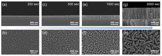
Figure 2.
SEM images of step-by-step nanowall growth. Four different sputtering deposition times, (a,b) 250 s (c,d) 500 s (e,f) 1000 s, and (g,h) 3000 s, show sequential growth of nanowalls from islands to thicker and taller nanowalls. (a,c,e,g) are cross section images and (b,d,f,h) are top-view images.
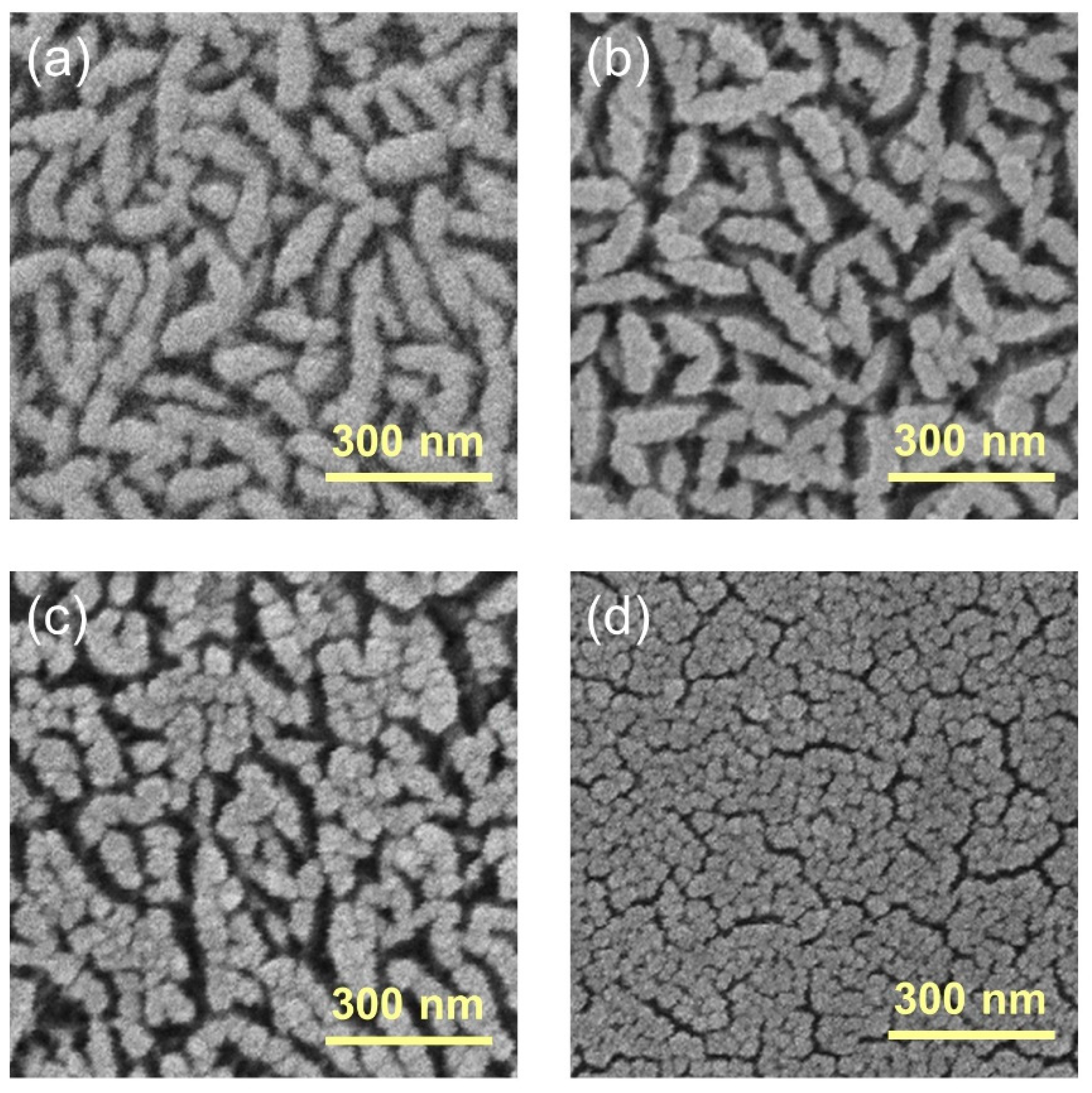
To confirm the annealing effect of the MoS2-MoSX nanowalls, RTA treatment with different temperatures, ranging from 200 °C to 500 °C, was performed for 10 min each on fully grown nanowalls (3000 s deposition time). Figure 3 shows the RTA treatment dependency as a function of RTA temperatures. Figure 3a–d correspond to visual identification of RTA temperatures ranging from 200 to 400 °C by FE-SEM images. At an annealing temperature of 200 °C, it is seen that the spacing of the nanowalls slightly increases, as shown in Figure 3b. It seems that the nanowalls are partially recrystallized. The nanowalls not only combine with the nearest walls but begin to re-crystallize at an annealing temperature of 300 °C, as shown in Figure 3c. When the annealing temperature is 400 °C, nanowalls appear to fully re-crystallize and combine with each other to create a thin film, as shown in Figure 3d. When the annealing temperature is increased further to 500 °C, the nanowalls fully melt and collapse, as shown in Figure S2b.
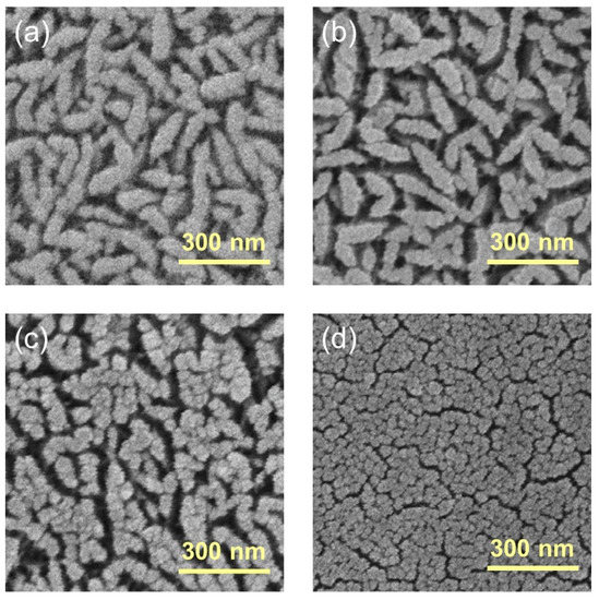
Figure 3.
Deformations of nanowalls according to the annealing temperature. SEM images of (a) as grown, (b) 200 °C rapid thermal annealing (RTA) treatment, (c) 300 °C RTA treatment, and (d) 400 °C RTA treatment samples.
To investigate the annealing effect of MoS2-MoSX nanowalls, we performed XRD and XPS measurements shown in Figure 4a and Figure S3. In the as-grown MoS2-MoSX nanowall sample, a strong peak in the (100)-plane is observed and a weak and broad peak is also observed corresponding to the (008)-plane, which indicates nanowall growth preference in the (100) direction (JCPDS Card No. 75-1539). As the annealing temperature increases to 400 °C, the peak in the (100)-plane is more enhanced and a new peak appears at the (002)-plane. This new peak is remarkably enhanced with increasing annealing temperature. When the temperature is further increased to 500 °C, a new peak occurs again around 26.5°, which is assumed to be the (040)-peak of MoO3 [6,36,37]. This can also be confirmed by XPS analysis. Figure S3 shows XPS narrow-scan spectra of the Mo 3d and S 2p before and after the annealing process. The MoOX peak rapidly increases after 500 °C annealing process. This result supports that the newly formed XRD peak after 500 °C annealing is MoO3. We estimate that the sulfur atoms on the surface of the MoS2 nanowalls evaporate in the RTA chamber during the high-temperature annealing process, resulting on sulfur vacancies on the MoS2-MoSX nanowalls [38,39]. When the annealed sample is placed in atmosphere after the RTA process, the (040) peak of MoO3 is generated by reacting with oxygen.
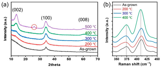
Figure 4.
(a) X-ray diffraction (XRD) spectra and (b) Raman shift as a function of annealing temperatures.
For a better understanding of the annealing effect, we also performed Raman spectra measurements, as shown in Figure 4b. The two main Raman peaks corresponding to and are clearly observed in all cases, depending on the annealing temperature. In the as-grown sample, two peaks are observed at 374.4 cm−1 and 411.2 cm−1; the frequency difference of these two Raman peaks is 36.9 cm−1. After annealing at 200 °C and 300 °C, a slight blue shift is observed in the peak. When the annealing temperature was increased to 400 °C, the intensity of the peak is increased; the peak is red-shifted (374.5 cm−1) and the peak is blue-shifted (408.4 cm−1). The frequency difference of the two Raman peaks is 33.9 cm−1 for this RTA temperature, which is less than that of the as-grown sample. This suggests that the crystallinity of annealed nanowalls is improved, which is in agreement with the XRD results in Figure 4a. Compared with single crystal monolayer MoS2 peaks [32,40], the observed Raman peaks show a blue shift for peaks and broadening at both peaks. The peak is associated with in-plane motion of Mo and S, in opposite directions, and the peak is associated with out-of-plane motion of S atoms [16]. Similar shifts and broadening results have been reported in previous papers [16,17,20,21,34]. The blue shift and asymmetric broadening can be associated with several effects from structural parameters, defects, size, crystallinity, elemental composition, etc [16,21,40]. Our nanowalls have a polycrystal structure, different wall sizes, and possibly contain different elemental compositions, such as MoS2, MoSX and MoOX.
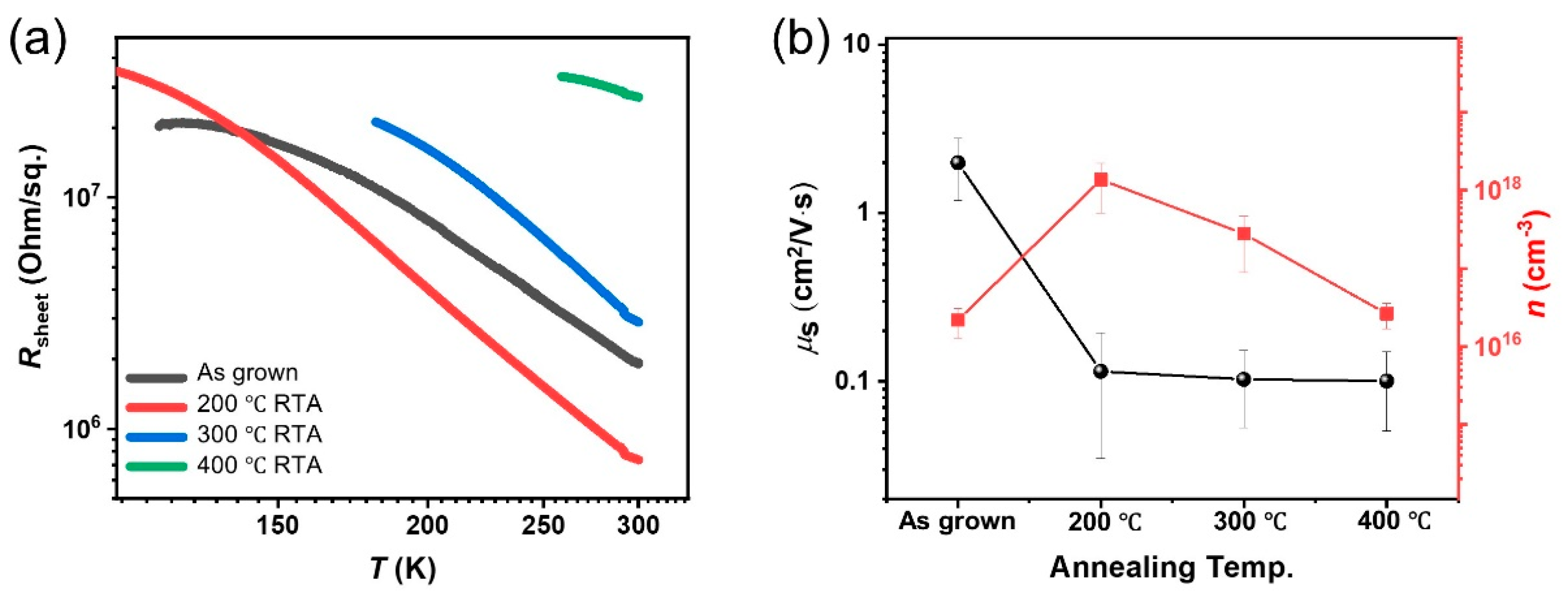
Next, the response of electrical properties to a perpendicular magnetic field were studied. Figure 5a shows sheet resistance trends as a function of measurement temperature. All resistance was measured while decreasing temperature and using the VDP geometry (5 mm-square samples). The data is displayed in log scale for both the temperature (x-axis) and sheet resistance (y-axis). As the sample temperature decreases, the sheet resistance behavior shows a higher-order trend, which has quadratic-like behavior in agreement with conventional semiconductor performance, for all samples. As shown in Figure 5a, the slope of the temperature dependent sheet resistance has the lowest value for the as-grown sample, which has the maximum value of residual resistance ratio (RRR) [R(300 K)/R(200 K) = 0.24] among the four samples. The other RRR values were 0.18 [R(300 K)/R(200 K)] at 200 °C RTA and 0.18 [R(300 K)/R(200 K)] at 300 °C RTA. The 400 °C RTA sample already reached the voltage detection limit at ~250 K.
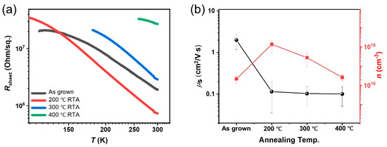
Figure 5.
(a) Temperature dependent sheet resistance and (b) Hall mobility and carrier concentrations at 300 K for four nanowall samples (as grown and RTA at 200 °C, 300 °C, and 400 °C for 10 min).
The RRR can be strongly affected by the amount of impurities and other crystallographic defects. It indirectly represents the purity and overall quality of a sample [41,42]. The RRR value for 200 °C and 300 °C RTA samples indicate that they have better crystallinity than the as-grown sample. The 400 °C RTA sample has different phases of crystallinity and conductance due to the melt-and-recrystallization procedure. Furthermore, the obtained sheet mobility (µ) and carrier concentration (n) show reasonable behavior of the higher mobility but lower carrier concentration at as-grown sample and lower mobility but higher carrier concentration at 200 °C and 300 °C RTA samples (Figure 5b). However, the 400 °C RTA sample has both low mobility and carrier concentration, which may be due to changes in elemental composition and nanowalls structure by the recrystallization process. In this study, all samples show the independently grown nanostructures, which are not connected to each other, not the form of a film in which the grains are connected. This structural effect makes the long and complex pathway for carrier transport, which is the reason that all samples show lower mobility values compared to previous reports [6,26].
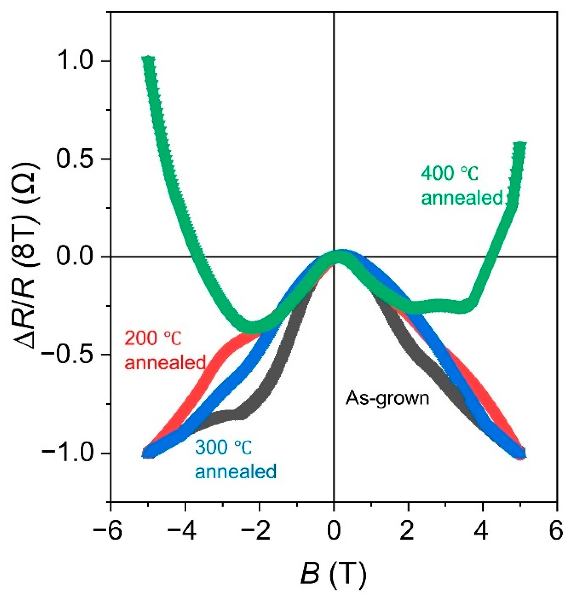
Furthermore, we studied magnetoresistance behavior as a function of perpendicular magnetic field sweep. All data were obtained using samples with a 5 mm-square geometry and four-probe measurements. Note that all magnetoresistance behavior is not smooth and shows less-quadratic trends because of the geometrical effect during the electromagnetic response measurement, which is caused by side carrier transport. As plotted in Figure 6, the magnetoresistance behavior mostly exhibits negative magnetoresistance behavior except for the 400 °C RTA sample. Negative magnetoresistance represents higher defects, disorder, and complicated diffusive carrier transport in crystalline materials [43,44,45,46]. This negative magnetoresistance behavior observed in three samples, from as-grown to 300 °C RTA, corresponds with high defect density caused by the nanowall structures. The 400 °C RTA annealed sample shows decreased negative magnetoresistance and close to conventional magnetoresistance (quadratic behavior with increasing magnetic field originated by cyclotron motion) at the higher magnetic field regime (approximately more than 3 T). This dramatic change for the 400 °C RTA sample is also in agreement with its film-like structure and phase transform due to the melt-and-recrystallization procedure. Thus, we can control electromagnetic response by tuning the post-annealing temperature and/or conditions.
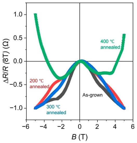
Figure 6.
Magnetoresistance behavior of samples (as grown, 200 °C, 300 °C, and 400 °C RTA for 10 min) at 300 K. Magnetoresistance values are normalized with ΔR divided by R (at 5 T).
4. Conclusions
We have shown the direct growth of MoS2 nanowalls via a sputtering deposition method and indicated the possibility of electronic transport tuning by investigating MoS2 nanowall electromagnetic properties. The MoS2-MoSX nanowall growth behavior was studied by changing growth time and the RTA process. All samples show exponential resistance increase with decreasing temperature, which corresponds to conventional low bandgap semiconductor behavior. The ~ 750 nm-thick MoS2-MoSX nanowalls have sheet carrier mobilities up to 2 cm2·V−1·s−1 and bulk carrier concentrations ranging from ~1017–1019 cm−3 depending on the RTA temperature. Moreover, perpendicular field dependent magnetoresistance at 300 K shows negative magnetoresistance behavior, which indicates resistance decay by an applied magnetic field. Interestingly, the 400 °C RTA samples show resistance upturn when applying an external magnetic field of more than 3 T. These results suggest the possible tuneability of MoS2 nanowall size and mesoscopic electronic transport properties.
Supplementary Materials
The following are available online at https://www.mdpi.com/article/10.3390/cryst11040351/s1. Figure S1: Large area growth of MoS2-MoSX nano-walls on 6-inch wafer. Figure S2: Fully Melted and collapsed MoS2-MoSX nano-walls at an annealing temperature of 500 °C., Figure S3: XPS narrow scan spectra of MoS2-MoSX nanowalls before and after annealing at 500 °C.
Author Contributions
Conceptualization, D.-S.U., J.-C.W., D.-P.K. and G.-H.K.; methodology, D.-S.U., J.-C.W., D.-P.K. and G.-H.K.; validation, D.-S.U., M.-J.J. and G.-H.K.; formal analysis, D.-S.U., M.-J.J., J.P. and Y.J.; data curation, D.-S.U., M.-J.J., J.P., Y.J. and G.-H.K.; writing-original draft preparation, D.-S.U. and M.-J.J.; writing-review and editing, D.-S.U. and G.-H.K.; visualization, D.-S.U., M.-J.J. and G.-H.K.; project administration, G.-H.K.; funding acquisition, G.-H.K. All authors have read and agreed to the published version of the manuscript.
Funding
The authors acknowledge support from the soft chemical materials research center for organic-inorganic multi-dimensional structures, which is funded by Gyeonggi Regional Research Center Program (Dankook 2016-B01). This work was also supported by the National Research Foundation of Korea (NRF-2018R1D1A1B07051202 and NRF-2020R1G1A1102692).
Institutional Review Board Statement
Not applicable.
Informed Consent Statement
Not applicable.
Data Availability Statement
The data presented in this study are available on request from the corresponding author.
Conflicts of Interest
The authors declare no conflict of interest.
References
- Wang, H.; Yuan, H.; Sae Hong, S.; Li, Y.; Cui, Y. Physical and chemical tuning of two-dimensional transition metal dichalcogenides. Chem. Soc. Rev. 2015, 44, 2664–2680. [Google Scholar] [CrossRef] [PubMed]
- Ryder, C.R.; Wood, J.D.; Wells, S.A.; Hersam, M.C. Chemically Tailoring Semiconducting Two-Dimensional Transition Metal Dichalcogenides and Black Phosphorus. ACS Nano 2016, 10, 3900–3917. [Google Scholar] [CrossRef]
- Lv, R.; Robinson, J.A.; Schaak, R.E.; Sun, D.; Sun, Y.; Mallouk, T.E.; Terrones, M. Transition metal dichalcogenides and beyond: Synthesis, properties, and applications of single- and few-layer nanosheets. Acc. Chem. Res. 2015, 48, 56–64. [Google Scholar] [CrossRef] [PubMed]
- Costanzo, D.; Jo, S.; Berger, H.; Morpurgo, A.F. Gate-induced superconductivity in atomically thin MoS2 crystals. Nat. Nanotechnol. 2016, 11, 339–344. [Google Scholar] [CrossRef]
- Hussain, S.; Shehzad, M.A.; Vikraman, D.; Khan, M.F.; Singh, J.; Choi, D.C.; Seo, Y.; Eom, J.; Lee, W.G.; Jung, J. Synthesis and characterization of large-area and continuous MoS2 atomic layers by RF magnetron sputtering. Nanoscale 2016, 8, 4340–4347. [Google Scholar] [CrossRef] [PubMed]
- Hussain, S.; Singh, J.; Vikraman, D.; Singh, A.K.; Iqbal, M.Z.; Khan, M.F.; Kumar, P.; Choi, D.C.; Song, W.; An, K.S.; et al. Large-area, continuous and high electrical performances of bilayer to few layers MoS2 fabricated by RF sputtering via post-deposition annealing method. Sci. Rep. 2016, 6, 30791. [Google Scholar] [CrossRef]
- Wang, Y.; Wang, S.; Li, C.; Qian, M.; Bu, J.; Wang, J.; Huang, R. Facile growth of well-dispersed and ultra-small MoS2 nanodots in ordered mesoporous silica nanoparticles. Chem. Commun. 2016, 52, 10217–10220. [Google Scholar] [CrossRef]
- Kalanyan, B.; Kimes, W.A.; Beams, R.; Stranick, S.J.; Garratt, E.; Kalish, I.; Davydov, A.V.; Kanjolia, R.K.; Maslar, J.E. Rapid Wafer-Scale Growth of Polycrystalline 2H-MoS2 by Pulsed Metalorganic Chemical Vapor Deposition. Chem. Mater. 2017, 29, 6279–6288. [Google Scholar] [CrossRef]
- Hu, C.; Jiang, Z.; Zhou, W.; Guo, M.; Yu, T.; Luo, X.; Yuan, C. Wafer-Scale Sulfur Vacancy-Rich Monolayer MoS2 for Massive Hydrogen Production. J. Phys. Chem. Lett. 2019, 10, 4763–4768. [Google Scholar] [CrossRef]
- Kim, Y.; Bark, H.; Kang, B.; Lee, C. Wafer-Scale Substitutional Doping of Monolayer MoS2 Films for High-Performance Optoelectronic Devices. ACS Appl. Mater. Interfaces 2019, 11, 12613–12621. [Google Scholar] [CrossRef]
- Krishnan, U.; Kaur, M.; Singh, K.; Kumar, M.; Kumar, A. A synoptic review of MoS2: Synthesis to applications. Superlattices Microstruct. 2019, 128, 274–297. [Google Scholar] [CrossRef]
- Song, B.; Gu, H.; Fang, M.; Chen, X.; Jiang, H.; Wang, R.; Zhai, T.; Ho, Y.-T.; Liu, S. Layer-Dependent Dielectric Function of Wafer-Scale 2D MoS2. Adv. Opt. Mater. 2019, 7, 1801250. [Google Scholar] [CrossRef]
- Sharma, A.; Mahlouji, R.; Wu, L.; Verheijen, M.A.; Vandalon, V.; Balasubramanyam, S.; Hofmann, J.P.; Erwin Kessels, W.M.M.; Bol, A.A. Large area, patterned growth of 2D MoS2 and lateral MoS2-WS2 heterostructures for nano- and opto-electronic applications. Nanotechnology 2020, 31, 255603. [Google Scholar] [CrossRef] [PubMed]
- Yoo, C.; Kaium, M.G.; Hurtado, L.; Li, H.; Rassay, S.; Ma, J.; Ko, T.J.; Han, S.S.; Shawkat, M.S.; Oh, K.H.; et al. Wafer-Scale Two-Dimensional MoS2 Layers Integrated on Cellulose Substrates Toward Environmentally Friendly Transient Electronic Devices. ACS Appl. Mater. Interfaces 2020, 12, 25200–25210. [Google Scholar] [CrossRef]
- Sari, F.N.I.; Ting, J.M. Direct Growth of MoS2 Nanowalls on Carbon Nanofibers for Use in Supercapacitor. Sci. Rep. 2017, 7, 5999. [Google Scholar] [CrossRef] [PubMed]
- Alexaki, K.; Kostopoulou, A.; Sygletou, M.; Kenanakis, G.; Stratakis, E. Unveiling the Structure of MoSx Nanocrystals Produced upon Laser Fragmentation of MoS2 Platelets. ACS Omega 2018, 3, 16728–16734. [Google Scholar] [CrossRef]
- Sreedhara, M.B.; Gope, S.; Vishal, B.; Datta, R.; Bhattacharyya, A.J.; Rao, C.N.R. Atomic layer deposition of crystalline epitaxial MoS2 nanowall networks exhibiting superior performance in thin-film rechargeable Na-ion batteries. J. Mater. Chem. A 2018, 6, 2302–2310. [Google Scholar] [CrossRef]
- Nawz, T.; Safdar, A.; Hussain, M.; Sung Lee, D.; Siyar, M. Graphene to Advanced MoS2: A Review of Structure, Synthesis, and Optoelectronic Device Application. Crystals 2020, 10, 902. [Google Scholar] [CrossRef]
- Yu, B.; Chen, Y.; Wang, Z.; Chen, D.; Wang, X.; Zhang, W.; He, J.; He, W. 1T-MoS2 nanotubes wrapped with N-doped graphene as highly-efficient absorbent and electrocatalyst for Li–S batteries. J. Power Sources 2020, 447, 227364. [Google Scholar] [CrossRef]
- Yang, P.; Zhang, Z.; Sun, M.; Lin, F.; Cheng, T.; Shi, J.; Xie, C.; Shi, Y.; Jiang, S.; Huan, Y.; et al. Thickness Tunable Wedding-Cake-like MoS2 Flakes for High-Performance Optoelectronics. ACS Nano 2019, 13, 3649–3658. [Google Scholar] [CrossRef]
- Kong, D.; Wang, H.; Cha, J.J.; Pasta, M.; Koski, K.J.; Yao, J.; Cui, Y. Synthesis of MoS2 and MoSe2 films with vertically aligned layers. Nano Lett. 2013, 13, 1341–1347. [Google Scholar] [CrossRef] [PubMed]
- Lin, Z.Y.; Liu, Y.; Halim, U.; Ding, M.N.; Liu, Y.Y.; Wang, Y.L.; Jia, C.C.; Chen, P.; Duan, X.D.; Wang, C.; et al. Solution-processable 2D semiconductors for high-performance large-area electronics. Nature 2018, 562, 254–258. [Google Scholar] [CrossRef]
- Kim, S.; Konar, A.; Hwang, W.S.; Lee, J.H.; Lee, J.; Yang, J.; Jung, C.; Kim, H.; Yoo, J.B.; Choi, J.Y.; et al. High-mobility and low-power thin-film transistors based on multilayer MoS2 crystals. Nat. Commun. 2012, 3, 1–7. [Google Scholar] [CrossRef]
- Chang, H.Y.; Yogeesh, M.N.; Ghosh, R.; Rai, A.; Sanne, A.; Yang, S.X.; Lu, N.S.; Banerjee, S.K.; Akinwande, D. Large-Area Monolayer MoS2 for Flexible Low-Power RF Nanoelectronics in the GHz Regime. Adv. Mater. 2016, 28, 1818–1823. [Google Scholar] [CrossRef]
- Bertolazzi, S.; Krasnozhon, D.; Kis, A. Nonvolatile Memory Cells Based on MoS2/Graphene Heterostructures. ACS Nano 2013, 7, 3246–3252. [Google Scholar] [CrossRef]
- Tao, J.G.; Chai, J.W.; Lu, X.; Wong, L.M.; Wong, T.I.; Pan, J.S.; Xiong, Q.H.; Chi, D.Z.; Wang, S.J. Growth of wafer-scale MoS2 monolayer by magnetron sputtering. Nanoscale 2015, 7, 2497–2503. [Google Scholar] [CrossRef]
- Chen, C.-A.; Lee, C.-L.; Yang, P.-K.; Tsai, D.-S.; Lee, C.-P. Active Site Engineering on Two-Dimensional-Layered Transition Metal Dichalcogenides for Electrochemical Energy Applications: A Mini-Review. Catalysts 2021, 11, 151. [Google Scholar] [CrossRef]
- Nalwa, H.S. A review of molybdenum disulfide (MoS2) based photodetectors: From ultra-broadband, self-powered to flexible devices. Rsc Adv. 2020, 10, 30529–30602. [Google Scholar] [CrossRef]
- Wang, L.; Jie, J.S.; Shao, Z.B.; Zhang, Q.; Zhang, X.H.; Wang, Y.M.; Sun, Z.; Lee, S.T. MoS2/Si Heterojunction with Vertically Standing Layered Structure for Ultrafast, High-Detectivity, Self-Driven Visible-Near Infrared Photodetectors. Adv. Funct. Mater. 2015, 25, 2910–2919. [Google Scholar] [CrossRef]
- Um, D.S.; Lee, Y.; Lim, S.; Park, S.; Lee, H.; Koe, H. High-Performance MoS2/CuO Nanosheet-on-One-Dimensional Heterojunction Photodetectors. ACS Appl. Mater. Inter. 2016, 8, 33955–33962. [Google Scholar] [CrossRef]
- Kim, H.S.; Kumar, M.D.; Kim, J.; Lim, D. Vertical growth of MoS2 layers by sputtering method for efficient photoelectric application. Sens. Actuat. A-Phys. 2018, 269, 355–362. [Google Scholar] [CrossRef]
- Shao, Q.; Yu, G.; Lan, Y.W.; Shi, Y.; Li, M.Y.; Zheng, C.; Zhu, X.; Li, L.J.; Amiri, P.K.; Wang, K.L. Strong Rashba-Edelstein Effect-Induced Spin-Orbit Torques in Monolayer Transition Metal Dichalcogenide/Ferromagnet Bilayers. Nano Lett. 2016, 16, 7514–7520. [Google Scholar] [CrossRef]
- Zhang, W.; Sklenar, J.; Hsu, B.; Jiang, W.; Jungfleisch, M.B.; Xiao, J.; Fradin, F.Y.; Liu, Y.; Pearson, J.E.; Ketterson, J.B.; et al. Research Update: Spin transfer torques in permalloy on monolayer MoS2. APL Mater. 2016, 4, 032302. [Google Scholar] [CrossRef]
- Jie, W.; Yang, Z.; Zhang, F.; Bai, G.; Leung, C.W.; Hao, J. Observation of Room-Temperature Magnetoresistance in Monolayer MoS2 by Ferromagnetic Gating. ACS Nano 2017, 11, 6950–6958. [Google Scholar] [CrossRef] [PubMed]
- Zhou, J.; Qiao, J.; Duan, C.G.; Bournel, A.; Wang, K.L.; Zhao, W. Large Tunneling Magnetoresistance in VSe2/MoS2 Magnetic Tunnel Junction. ACS Appl. Mater. Interfaces 2019, 11, 17647–17653. [Google Scholar] [CrossRef] [PubMed]
- Bai, S.L.; Chen, C.; Luo, R.X.; Chen, A.F.; Li, D.Q. Synthesis of MoO3/reduced graphene oxide hybrids and mechanism of enhancing H2S sensing performances. Sens. Actuat. B-Chem. 2015, 216, 113–120. [Google Scholar] [CrossRef]
- Liu, Y.; Feng, P.Z.; Wang, Z.; Jiao, X.Y.; Akhtar, F. Novel Fabrication and Enhanced Photocatalytic MB Degradation of Hierarchical Porous Monoliths of MoO3 Nanoplates. Sci. Rep. 2017, 7, 1845. [Google Scholar] [CrossRef]
- Liu, M.X.; Shi, J.P.; Li, Y.C.; Zhou, X.B.; Ma, D.L.; Qi, Y.; Zhang, Y.F.; Liu, Z.F. Temperature-Triggered Sulfur Vacancy Evolution in Monolayer MoS2/Graphene Heterostructures. Small 2017, 13, 1602967. [Google Scholar] [CrossRef]
- Ishihara, S.; Hibino, Y.; Sawamoto, N.; Suda, K.; Ohashi, T.; Matsuura, K.; Machida, H.; Ishikawa, M.; Sudoh, H.; Wakabayashi, H.; et al. Improving crystalline quality of sputtering-deposited MoS2 thin film by postdeposition sulfurization annealing using (t-C4H9)2S2. Jpn. J. Appl. Phys. 2016, 55, 04EJ07. [Google Scholar] [CrossRef]
- Li, H.; Zhang, Q.; Yap, C.C.R.; Tay, B.K.; Edwin, T.H.T.; Olivier, A.; Baillargeat, D. From Bulk to Monolayer MoS2: Evolution of Raman Scattering. Adv. Funct. Mater. 2012, 22, 1385–1390. [Google Scholar] [CrossRef]
- Murase, S.; Ogawa, R.; Saitoh, T.; Moriai, H.; Matsushita, T.; Osamura, K. Residual Resistance Ratio Measurement Method of Cu/Nb3Sn Composite Conductors; Springer: Tokyo, Japan, 2000; pp. 700–702. [Google Scholar]
- Charifoulline, Z. Residual Resistivity Ratio (RRR) Measurements of LHC Superconducting NbTi Cable Strands. IEEE Trans. Appl. Supercond. 2006, 16, 1188–1191. [Google Scholar] [CrossRef]
- Eisele, I.; Dorda, G. Negative Magnetoresistance in n-Channel (100) Silicon Inversion Layers. Phys. Rev. Lett. 1974, 32, 1360–1363. [Google Scholar] [CrossRef]
- Bishop, D.J.; Dynes, R.C.; Tsui, D.C. Magnetoresistance in Si metal-oxide-semiconductor field-effect transitors: Evidence of weak localization and correlation. Phys. Rev. B 1982, 26, 773–779. [Google Scholar] [CrossRef]
- Hishiyama, Y.; Kaburagi, Y.; Inagaki, M. Chapter 9—Magnetoresistance. In Materials Science and Engineering of Carbon; Inagaki, M., Kang, F., Eds.; Butterworth-Heinemann: Oxford, UK, 2016; pp. 173–204. [Google Scholar]
- Breunig, O.; Wang, Z.; Taskin, A.A.; Lux, J.; Rosch, A.; Ando, Y. Gigantic negative magnetoresistance in the bulk of a disordered topological insulator. Nat. Commun. 2017, 8, 15545. [Google Scholar] [CrossRef]
Publisher’s Note: MDPI stays neutral with regard to jurisdictional claims in published maps and institutional affiliations. |
© 2021 by the authors. Licensee MDPI, Basel, Switzerland. This article is an open access article distributed under the terms and conditions of the Creative Commons Attribution (CC BY) license (http://creativecommons.org/licenses/by/4.0/).

