Article

Terahertz Emission and Ultrafast Carrier Dynamics of Ar-Ion Implanted Cu(In,Ga)Se2 Thin Films

1
Integrated Optics Laboratory, Advanced Photonics Research Institute, Gwangju Institute Science and Technology, Gwangju 61105, Korea
2
Research Group of Consumer Safety, Korea Food Research Institute, Jeonju 55365, Korea
3
ICT Materials Technology Research Laboratory, Electronics and Telecommunications Research Institute, Daejeon 34129, Korea
4
YUHS-KRIBB, Medical Convergence Research Institute, College of Medicine, Yonsei University, Seoul 03722, Korea
5
Department of Advanced Device Technology, Korea University of Science and Technology, Daejeon 34113, Korea
*
Authors to whom correspondence should be addressed.
Crystals 2021, 11(4), 411; https://doi.org/10.3390/cryst11040411
Submission received: 17 February 2021 / Revised: 8 April 2021 / Accepted: 8 April 2021 / Published: 12 April 2021
(This article belongs to the Special Issue Investgation of Molecular by Terahertz Spectroscopy)

Abstract

:
We investigated THz emission from Ar-ion-implanted Cu(In,Ga)Se2 (CIGS) films. THz radiation from the CIGS films increases as the density of implanted Ar ions increases. This is because Ar ions contribute to an increase in the surface surge current density. The effect of Ar-ion implantation on the carrier dynamics of CIGS films was also investigated using optical pump THz probe spectroscopy. The fitted results imply that implanted Ar ions increase the charge transition of intra-and carrier–carrier scattering lifetimes and decrease the bandgap transition lifetime.

1. Introduction

Copper indium gallium diselenide (CIGS) thin films are considered good candidates for semiconductor-based solar cells, because they are capable of large-area fabrication and have a high energy conversion efficiency and flexibility. They are extensively used in the space of solar cell applications in particular, owing to their flexibility and large-area fabrication [1,2,3,4]. Recent research on CIGS reveals that their conversion efficiency exceeds 23% [5].
Ion implantation can change the properties of solid materials according to the energy that accelerates one elemental ion without heat treatment or compounding [6]. Therefore, ion implantation can be widely used to change the physical and chemical properties of various solid structures. Ion implantation is an extremely useful tool, particularly for controlling the electrical properties of semiconductor surfaces [7]. Thus, it can be utilized as an alternative to adjust the electrical and optical properties of semiconducting thin film materials such as CIGS. Gas ion implantation is good specifically for controlling the properties because of the depth of gas ionization around a few μm [3,4].
Terahertz (THz) technologies are powerful tools for characterizing the electrodynamics of the carriers and optical properties of semiconductors and nanomaterials non-destructively [8,9]. In the case of THz emission spectroscopy, we can observe the current characteristics and charge transfer of the surface and bulk [10,11]. THz time-domain spectroscopy can be used to measure the optical transmittance, complex optical and dielectric constants, and ac conductivity of matters in the THz frequency region [8,9]. Optical pump THz probe spectroscopy can detect carrier dynamics, spin motion, and charge transfer in the semiconductor and dielectric matter according to the energy of the excitation beam [12,13,14]. Recently, the carrier dynamics of CIGS thin films were actively investigated using optical pump THz probe spectroscopy to interpret the behavior of several defects distributed in CIGS thin films [14,15,16]. Thus, THz spectroscopy studies on the carrier dynamics of ion-implanted CIGS films would be significant.
In this study, the electrical properties and carrier dynamics of Ar-ion-implanted CIGS thin films were investigated using THz emission and optical pump THz probe spectroscopy. Ar ion can affect the surface of CIGS rather than light ions, for example, H ion [17] because Ar ion weighs more than H-ion.
Therefore, Ar-ion implantation can directly affect the surface damage of CIGS films. Enhanced THz emission from Ar-ion-implanted CIGS films was observed. This is because the implanted Ar ions increase the participation of surface carriers in the transient surface current generating THz radiation. The carrier dynamics of the CIGS films were investigated by optical pump THz probe spectroscopy. Ar-ion implantation increases the term associated with fast decay but decreases the term associated with slow decay to affect the overall current flow.

2. Materials and Methods
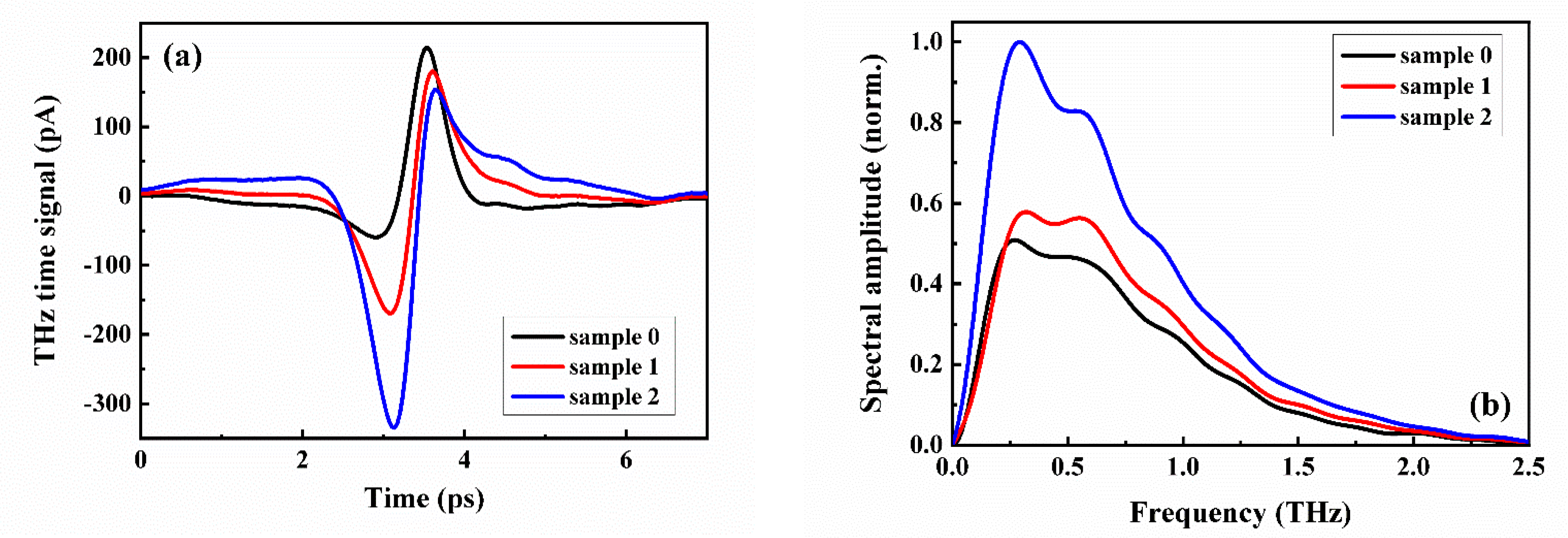
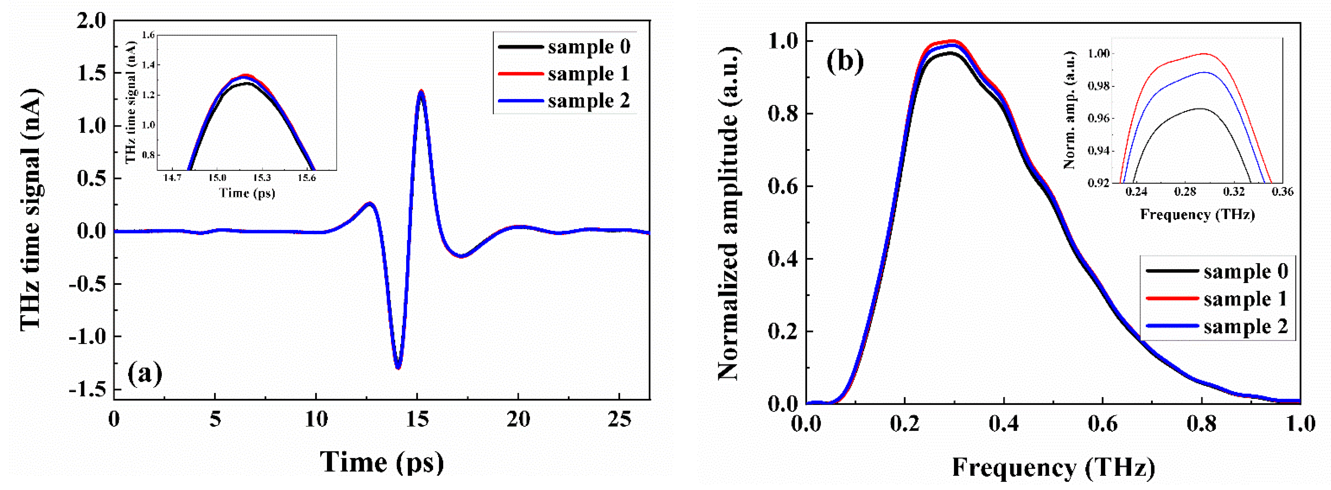
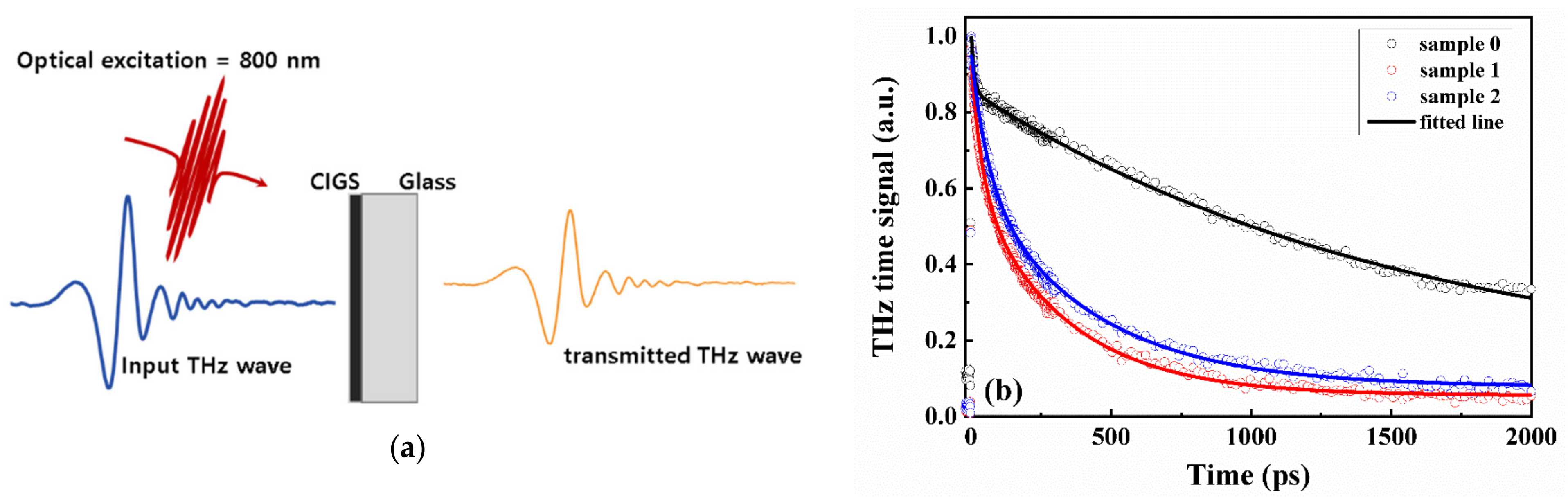
The CIGS thin film is directly deposited on a soda lime glass with a thickness of approximately 2 μm using a 3-stage co-evaporation system [18]. The composition ratios of Cu/III and Ga/III in the CIGS thin film were measured to be 1.02 and 0.33, respectively, by energy dispersive spectrometry. In general, the bandgap of CIGS is dependent on the ratio of In and Ga content from about 1 eV (CIS) to approximately 1.7 eV (CGS). In our sample, the bandgap is below 1.3 eV before Ar-ion implantation at 14 K [17].
Ar-ion implantation into CIGs thin film was carried out at the Korea Multi-purpose Accelerator Complex (KOMAC). The implantation densities of Ar ions were 1 × 10¹⁴/cm2 (sample 1) and 1 × 10¹⁶/cm2 (sample 2) with an energy of 200 keV. Two samples were prepared to investigate the changes the electrical and optical properties of the surfaces of the CIGS films according to the concentration. The implantation distribution of Ar ions was calculated using stopping and range of ions in matter (SRIM), which is generally used to calculate the interaction of ions with matter, based on the element ratio of the CIGS thin film. The calculation results demonstrate that the Ar-ion implantation is predominantly distributed in 1 μm of the 2 μm thick CIGS film (not shown here).

3. Results

Figure 1 presents the results of THz emission spectroscopy obtained from the CIGS thin film as a function of the Ar-ion implantation density. To radiate the THz waves on the CIGS thin films, a femtosecond laser with an 80 MHz repetition rate, 800 nm wavelength, and 100fs pulse width was illuminated on the samples. The input power was 350 mW, the incident angle was 45°, and the diameter was 5 mm. The detector for THz waves is used with a 5 μm dipole gap photoconductive antenna on a low-temperature grown GaAs substrate with 10 mW fs laser power.
Figure 2a displays the THz radiation waveforms of the CIGS film samples in the time domain. Sample 0 denotes a CIGS thin film without Ar-ion implantation. In the time-domain waveforms, the down-peak amplitudes decrease as the Ar-ion implantation density increases. The increment ratio of the down peak dramatically increases and the upper peak slightly decreases as the Ar-ion implantation density increases. Figure 2b depicts the frequency domain data acquired by fast Fourier transformation of the time-domain data. All data have frequency components up to 2.5 THz. The spectral amplitudes of the CIGS thin films increase as the Ar-ion implantation density increases.
THz transmission through samples were measured using THz time-domain spectroscopy. Figure 3a,b show the transmitted THz waveforms in time and spectral amplitudes of the THz waves, respectively. The results confirmed that the considered Ar-ion implantation density rarely changes the THz transmission.
To investigate the electrical properties, we performed Hall measurements for the samples. From the measurements, the carrier densities (mobilities) of samples 0, 1, and 2 are 1.57 (1.31), 3.45 (1.05), and 41.1 × 1017 cm−3 (0.057 cm2/V∙s), respectively. The Ar-ion implantation increases the carrier density but decreases the mobility because the implanted ions cause the defect sites to prevent the flow of current and increase the change in current in time. In general, THz radiation is dependent on the surge current of the surface of a semiconductor. The related equation is as follows [19]:
E T H z t d J d t E b d n t d t
ETHz is the THz radiation field, J is the surge current, Eb is the built-in surface field, and n is the carrier density. The build-in surface field is formed by the energy band bending at a surface. The implanted Ar ions increase the band bending and, thus, the build-in field [17]. Since the surge current of the surface is proportional to the carrier density, the Ar-ion implantation density-dependent THz emission from the samples reflects the Hall measurement results.
In order to investigate the effect of Ar ion implantation on the carrier dynamics in the CIGS films, we employed optical pump THz probe spectroscopy, which is widely used to observe the dynamics of charge in the fs to ps time region. The optical pump THz probe spectroscopy scheme is shown in Figure 4a,b and shows the decay of the upper peak amplitudes of the transmitted THz wave of the samples over time. We used a regenerative amplified fs laser system with a 1 kHz repetition rate of 800 nm. In order to generate and detect THz pulses, we used ZnTe crystals [17]. The shapes of the decay of the Ar-ion implanted samples are clearly different from that of sample 0. To analyze the difference, we employed bi-exponential decay functions to fit the decay curves [17,20].
A 1 × e x p t t 0 τ 1 + A 2 × e x p t t 0 τ 2 + y 0
where y0 and t0 are the offsets of the y and t values of the decay curve, respectively, while the absolute values of A1 and A2 are the amplitudes of the exponential terms having τ1 and τ2 decay time constants, respectively. The fitted results are summarized in Table 1. The τ1 and τ2 are considered to be determined by surface and bulk defect states, respectively, and depend on the quality of the CIGS thin film with respect to various defect densities [14,16,21]. The decay time constants of samples are similar to those of previous studies [22]. According to the fitting results, τ1 and τ2 increase as the density of Ar-ion increases. It was explained by the increase in the density of both surface and bulk defect states [14,16,21]. The τ1 is determined by the trapping time of photo-carriers from the conduction band to shallow defect states within several or tens of picoseconds. The τ2 denoted the averaged slow decay time captured at various defect states in the CIGS thin film [14,16,21]. The results show that not only surface defects but also bulk defect states are formed by the Ar-ion implantation, and the defect density depends on the concentration of the implanted Ar-ions.

4. Conclusions

We investigated the effect of Ar-ion implantation on the THz emission of CIGS films. THz emission from CIGS films increases as the density of implanted Ar ions increases because Ar ions increase the build-in surface field and density of the surface surge current. The effect of Ar-ion implantation on the carrier dynamics of CIGS films was also investigated using optical pump THz probe spectroscopy. The fitted results demonstrate that the surface and bulk defect states formed by the implanted Ar ions change the carrier lifetimes.

Author Contributions

Conceptualization, C.K., G.L., and W.-J.L.; methodology, I.M. and D.-H.C.; validation, C.K. and W.-J.L.; formal analysis, G.L.; writing—original draft preparation, C.K., G.L., and W.-J.L.; writing—review and editing, Y.-D.C. and C.-S.K.; project administration, Y.-D.C. and C.-S.K. All authors have read and agreed to the published version of the manuscript.

Funding

This work was supported by the Gwangju Institute of Science and Technology (GIST) Research Institute (GRI) grant funded by the GIST in 2021 and the Basic Science Research Program through the National Research Foundation of Korea (NRF) funded by the Ministry of Science and ICT (NRF-2019R1F1A1063156) and The Technology Development Program to Solve Climate Changes of the National Research Foundation (NRF) funded by the Ministry of Science, ICT and Future Planning (2016M1A2A2936754).

Conflicts of Interest

The authors declare no conflict of interest.

References

  1. Dabbabi, S.; Bennasr, T.; Kamoun, N.T. CIGS Solar Cells for Space Applications: Numerical Simulation of the Effect of Traps Created by High-Energy Electron and Proton Irradiation on the Performance of Solar Cells. JOM J. Miner. Met. Mater. Soc. 2019, 71, 602–607. [Google Scholar] [CrossRef]
  2. Otte, K.; Makhova, L.; Braun, A.; Konovalov, I. Flexible Cu(In,Ga)Se2 thin-film solar cells for space application. Thin Solid Films 2006, 511–512, 613–622. [Google Scholar] [CrossRef]
  3. Jasenek, A.; Schock, H.W.; Werner, J.H.; Rau, U. Defect annealing in Cu(In,Ga)Se2 heterojunction solar cells after high energy electron irradiation. Appl. Phys. Lett. 2001, 79, 2922. [Google Scholar] [CrossRef]
  4. Jasenek, A.; Rau, U. Defect generation in Cu(In,Ga)Se2 heterojunction solar cells by high-energy electron and proton irradiation. J. Appl. Phys. 2001, 90, 650. [Google Scholar] [CrossRef]
  5. Green, M.A.; Dunlop, E.D.; Hohl-Ebinger, J.; Yoshita, M.; Kopidakis, N.; Hao, X. Solar cell efficiency tables (version 56). Prog. Photovoltaics Res. Appl. 2020, 28, 629–638. [Google Scholar] [CrossRef]
  6. Mayer, J.W. Ion Implantation Semiconductors; Californian Institution of Technology: Pasadena, CA, USA, 1998. [Google Scholar]
  7. Larson, L.A.; Williams, J.M.; Michael, I. Current, Ion Implantation for Semiconductor Doping and Materials Modification. Rev. Accel. Sci. Technol. 2011, 4, 11–40. [Google Scholar] [CrossRef]
  8. Lee, S.H.; Choi, M.; Kim, T.T.; Lee, S.; Liu, M.; Yin, X.; Choi, H.K.; Lee, S.S.; Choi, C.-G.; Zhang, X.X.; et al. Switching terahertz waves with gate-controlled active graphene metamaterials. Nat. Mater. 2012, 11, 936–941. [Google Scholar] [CrossRef] [PubMed] [Green Version]
  9. Yoo, H.K.; Yoon, Y.; Lee, K.; Kang, C.; Kee, C.-S.; Hwang, I.-W.; Lee, J.W. Highly efficient terahertz wave modulators by photo-excitation of organics/silicon bilayers. Appl. Phys. Lett. 2014, 105, 011115. [Google Scholar] [CrossRef]
  10. Lee, W.J.; Ma, J.W.; Bae, J.M.; Jeong, K.S.; Cho, M.H.; Kang, C.; Wi, J.S. Strongly Enhanced THz Emission caused by Localized Surface Charges in Semiconducting Germanium Nanowires. Sci. Rep. 2013, 3, 1984. [Google Scholar] [CrossRef] [PubMed] [Green Version]
  11. Němec, H.; Pashkin, A.; Kužel, P.; Khazan, M.; Schnüll, S.; Wilke, I. Carrier dynamics in low-temperature grown GaAs studied by terahertz emission spectroscopy. J. Appl. Phys. 2001, 90, 1303. [Google Scholar] [CrossRef] [Green Version]
  12. George, P.A.; Strait, J.; Dawlaty, J.; Shivaraman, S.; Chandrashekhar, M.; Rana, F.; Spencer, M.G. Ultrafast Optical-Pump Terahertz-Probe Spectroscopy of the Carrier Relaxation and Recombination Dynamics in Epitaxial Graphene. Nano Lett. 2008, 8, 4248. [Google Scholar] [CrossRef] [PubMed] [Green Version]
  13. Averitt, R.D.; Rodriguez, G.; Siders, J.L.W.; Trugman, S.A.; Taylor, A.J. Conductivity artifacts in optical-pump THz-probe measurements of YBa2Cu3O7. J. Opt. Soc. Am. B Opt. Phys. 2000, 17, 327–331. [Google Scholar] [CrossRef]
  14. Lee, W.-J.; Cho, D.-H.; Wi, J.-H.; Han, W.S.; Chung, Y.-D.; Park, J.; Bae, J.M.; Cho, M.-H. Na-Dependent Ultrafast Carrier Dynamics of CdS/Cu(In,Ga)Se2 Measured by Optical Pump-Terahertz Probe Spectroscopy. J. Phys. Chem. C 2015, 119, 20231–20236. [Google Scholar] [CrossRef]
  15. Lee, W.-J.; Yu, H.-J.; Wi, J.-H.; Cho, D.-H.; Han, W.S.; Yoo, J.; Yi, Y.; Song, J.-H.; Chung, Y.-D. Behavior of Photocarriers in the Light-Induced Metastable State in the p-n Heterojunction of a Cu(In,Ga)Se2 Solar Cell with CBD-ZnS Buffer Layer. ACS Appl. Mater. Interfaces 2016, 8, 22151–22158. [Google Scholar] [CrossRef] [PubMed]
  16. Lee, W.-J.; Cho, D.-H.; Wi, J.-H.; Yu, H.-J.; Han, W.S.; Bae, J.M.; Park, J.; Chung, Y.-D. Ultrafast Photocarrier Dynamics at the p–n Junction in Cu(In,Ga)Se2 Solar Cell with Various Zn(O,S) Buffer Layers Measured by Optical Pump–Terahertz Probe Spectroscopy. ACS Appl. Energy Mater. 2018, 1, 522–530. [Google Scholar] [CrossRef]
  17. Lee, W.-J.; Lee, G.; Cho, D.-H.; Chul, K.; Myoung, N.; Kee, C.S.; Chung, Y.-D. Ultrafast Photoexcited-Carrier Behavior Induced by Hydrogen Ion Irradiation of a Cu(In,Ga)Se2 Thin Film in the Terahertz Region. IEEE Trans. Terahertz Sci. Technol. Early Access 2021. [Google Scholar] [CrossRef]
  18. Chung, Y.-D.; Cho, D.-H.; Han, W.-S.; Park, N.-M.; Lee, K.-S.; Kim, J. Incorporation of Cu in Cu(In,Ga)Se2-based Thin-film Solar Cells. J. Korean Phys. Soc. 2010, 57, 1826–1830. [Google Scholar] [CrossRef]
  19. Sakai, K. THz Optoelectronics, Topics in Applied Physics; Springer: Berlin/Heidelberg, Germany, 2005; Chapter 3. [Google Scholar]
  20. Liu, X.; Yu, H.; Ji, Q.; Gao, Z.; Ge, S.; Qiu, J.; Liu, Z.; Zhang, Y.; Sun, D. An ultrafast terahertz probe of the transient evolution of the charged and neutral phase of photo-excited electron-hole gas in a monolayer semiconductor. 2D Mater. 2016, 3, 014001. [Google Scholar] [CrossRef] [Green Version]
  21. Lee, W.-J.; Cho, D.-H.; Bae, J.M.; Kim, M.E.; Park, J.h.; Chung, Y.-D. Ultrafast wavelength-dependent carrier dynamics related to metastable defects in Cu(In,Ga)Se2 solar cells with chemically deposited Zn(O,S) buffer layer. Nano Energy 2020, 74, 104855. [Google Scholar] [CrossRef]
  22. Kushnir, K.; Wang, M.; Fitzgerald, P.D.; Koski, K.J.; Titova, L.V. Ultrafast zero-bias photocurrent in GeS nanosheets: Promise for photovoltaics. ACS Energy Lett. 2017, 2, 1429–1434. [Google Scholar] [CrossRef]
Figure 1. Schematic view of the THz time-domain spectroscopy system employed in the experiments.
Crystals 11 00411 g001
Figure 2. (a) Radiated THz waveforms of copper indium gallium diselenide (CIGS) thin films in time domain and (b) frequency domain waveforms of time-domain waveforms of CIGS thin films through fast Fourier transformation.
Crystals 11 00411 g002
Figure 3. (a) The transmitted THz time-domain waveforms of CIGS films by using the THz time-domain spectroscopy and (b) frequency domain waveforms of time-domain waveforms.
Crystals 11 00411 g003
Figure 4. (a) Scheme of optical pump THz probe measurement and (b) the decay of amplitudes of transmitted THz wave through samples measured by optical pump THz spectroscopy.
Crystals 11 00411 g004
Table 1. Fitted decay constants of samples.
Sample 0Sample 1Sample 2
τ19.9038.4359.44
τ21569.22328.45414.44
Publisher’s Note: MDPI stays neutral with regard to jurisdictional claims in published maps and institutional affiliations.

