Abstract
Mechanism of copper nanostructuring by oxides and hydroxide formation during anodizing is not fully understood. At the same time, the search for novel copper anodizing regimes and electrolytes is ongoing due to multiple potential applications. In this work copper anodizing in two electrode setups, in stirred 0.01 M solution of NaHCO3 at 20 °C and at voltages ranging from 5 to 40 V was explored. The morphology and composition of prepared materials were studied using FE-SEM imaging and XRD measurements. Anodizing at potentials in a range of 15–30 V led to formation of nanowires composed of crystalline Cu2O, CuO, Cu(OH)2 and malachite Cu2CO₃(OH)2. The latter was formed due to anion incorporation from the electrolyte. The diameter of nanowires strongly depended on the applied voltage, and was 35 ± 6 nm for samples prepared at 15 V, and 45 ± 9 nm for 30 V. At higher applied voltages oscillations of current density were observed, suggesting partial delamination of the formed oxidized layer, with subsequent self-healing.
1. Introduction
Copper surface nanostructuring with oxide layers is one of the approaches that could benefit numerous emerging applications, like: carbon dioxide reduction reaction (CO2RR) [1,2,3,4], photoelectrochemical water splitting [1,5], assembly of efficient batteries [1,6,7], photodegradation of pollutants [1,8], improved performance and lower costs of direct methanol fuel cells assembly [1,9,10], engineering of smart and corrosion resistant surfaces [1,11,12].
There are numerous methods of copper oxides nanostructuring, including: thermal annealing [13], hydrothermal methods [14,15], precipitation using colloids chemistry [16,17], sonochemical synthesis [18] and exploding wire technique [19], as well as anodizing [1,20]. The latter seems to be one of the least explored techniques for copper oxides formation, despite the fact that it could provide benefits like: high aspect ratio of the nanostructures, control of the morphology by adjusting the synthesis conditions and easy scaling up even to industrial scale.
Additionally, from the fundamental point of view, copper anodizing is an interesting issue itself. Mechanism of electrooxidative CuOx growth on Cu surface is yet not fully explored and it is much more complex when compared to anodization of other metals. Such a complex mechanism of copper anodizing has certain implications in morphology, chemical composition and crystallinity of the grown nanostructures. Typically, anodic oxides form hexagonally arranged nanopores [21,22,23,24] or nanotubes [25,26,27], while for anodic copper oxides/hydroxide nanowires, nanoneedles or nanorods morphology have been reported [28,29]. Only zinc anodizing leads to formation of nanowires similar to those grown via copper anodizing [30]. Nevertheless, in this particular case, when fluoride-based electrolytes were used, copper anodizing resulted in nanopores formation [29]. Furthermore, stoichiometry for majority of anodic oxides is fixed, i.e., Al2O3 [21,22,23,24], TiO2 [25,26], WO3 [27] or ZnO [30], while anodization of copper results in formation of three compounds simultaneously: Cu2O, CuO and Cu(OH)2 with various ratios between them [28,29]. Moreover, oxides formed via anodizing are typically amorphous with the only exception for anodically grown ZrO2 that is tetragonal or monoclinic [31]. Copper anodizing, however, enables formation of nanowires consisting of monoclinic tenorite—CuO, cubic cuprite—Cu2O, and usually amorphous Cu(OH)2 [28].
Aforementioned features of anodically grown CuOx/Cu(OH)2 nanostructures attract scientific attention, however copper anodizing is still neither fully understood nor explored. Therefore, studying new experimental conditions of the process -such as new electrolytes—is essential to acquire deeper insight into the phenomena behind formation of these nanostructures. So far, copper was reported to be anodized usually in aqueous alkaline electrolytes like NaOH [32] or KOH [33,34]. Recently also anodizing in aqueous solutions of salts with alkaline hydrolysis, such as K2CO3 [33], KHCO3 [34] and Na2CO3 was reported [28,35].
The main motivation of this research is to explore a new electrolyte for copper anodizing, namely 0.01 M NaHCO3. Studies on crystallinity of the formed nanostructures, accompanied by quantitative image analysis provide valuable insight into new anodizing regimes. Additionally, limitations of copper anodizing in sodium bicarbonate solutions are shown and discussed.
2. Materials and Methods
High-purity (99.9999%) 0.25 mm thick copper foil (Puratronic, Alfa-Aesar) was cut into 10 × 25 mm coupons and degreased with acetone and ethanol. The samples were electropolished at 10 V in 10 M H3PO4 at 20 °C for 4 min. with stirring. Afterwards, back side and edges of each sample were coated with protective paint in order to limit the working area of each sample to 1 cm2.
Before anodizing, the samples were dipped for ca. 2 s in concentrated HCl to remove any native oxides at the surface of Cu, and subsequently thoroughly washed in DI water.
Anodizations were performed in a typical two-electrode setup, where Pt mesh was used as a cathode and a copper sample served as anode. The experiments were performed in vigorously stirred 0.01 M NaHCO3 at 20 °C and at voltages ranging from 5 to 40 V (5 V step) for 2 h. Current density transients were recorded using APPA 208 multimeters with 1 Hz frequency. For each experiment, a fresh portion of an electrolyte was used to avoid redeposition of copper species remaining in the solution from previous experiments [35]. It is important to note that in the case of copper anodizing hydrodynamics of the electrochemical cell is crucial. In reported experiments, the distance between electrodes was kept constant, at 3 cm and the stirring was vigorous, providing vortex. Anode and cathode were placed on the opposite sides of the vortex.
Morphology of the prepared material was investigated using Zeiss 1550 Field Emission Scanning Electron Microscope (FE-SEM, Eindhoven, The Netherlands). Diameters of the obtained nanostructures were assessed using three FE-SEM images taken in random sections. The quantitative image analyses were performed using ImageJ freeware. For each sample 100 independent measurements were performed, and the results are presented as an average ± standard deviation. The measurements were taken individually, from original images, without any thresholding, nor binarization.
The X-ray diffraction (XRD) experiments of all as-prepared samples were conducted using Rigaku ULTIMA IV diffractometer (Rigaku, Tokyo, Japan) equipped with CoKα radiation source within the 2θ range of 20°–50°, with a step size of 0.02° and an acquisition rate of 1° per minute. The recorded data was processed using Origin® software (Original Lab, Origin Pro 8, North Hampton, NH, USA) and crystalline phases were identified based on the COD crystallographic database with Match software (Crystal Impact, v 3.11.3.192, Bonn, Germany). The XRD patterns have been normalized to the most intensive reflex in each pattern.
3. Results and Discussion
3.1. Current Density Transients
Figure 1 shows current density transients recorded during copper anodizing in 0.01 M NaHCO3 for 2 h.
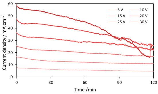
Figure 1.
Current density transients recorded during 2 h long copper anodizations in 0.01 M NaHCO3 performed at 5, 10, 15, 20, 25 and 30 V.
It is apparent that during the first 2 min there is a rapid drop in current density followed by short plateau (especially for greater voltages). Presumably, in this initial phase, anodic oxide coats the entire Cu surface. According to Giri and Sarkar [36], electrochemical oxidation of copper might lead to the formation of Cu2O and CuO, where CuO could be generated through both copper and Cu2O oxidation. Thus, it can be stated, Cu2O formation is the first stage of copper anodizing, and can be represented by following electrochemical and chemical reactions (Equations (1)–(3)) [36]:
In further stages, both Cu2O and CuO are formed directly by metallic copper oxidation. Simultaneously, Cu2O undergoes consecutive conversion and Cu(I) species and can be partially consumed to form CuO, according to the following reactions (Equations (4)–(7)) [36]:
Afterwards, copper oxides and hydroxide growth continues and copper is consumed for both Cu(I) and Cu(II) compounds formation with partial Cu(I) consumption to form Cu(II) species. Additionally, in alkaline environment, Cu(II) species might form water soluble coordination anions according to (Equations (8)–(10)) [36]:
Simultaneously, there is a local pH drop at the anode (Equation (11)):
And Cu(II) species redeposition at the electrode surface might occur (Equation (12)):
What is more, Cu(OH)2 might decompose forming CuO (Equation (13)):
The gradual drop of current density is caused by the growth of the oxide layer. Both copper oxides are semiconductors with band gaps equal to 2.19–2.29 and 1.44 eV for Cu2O and CuO, respectively. Therefore, CuOx layer formed at the metallic Cu surface increases electric resistance of the anode [37]. However, after a certain time, further drop accompanied by current oscillations is noticed (Figure 1 and Figure S1 (Supplementary Materials)). The greater the applied voltage the sooner this drop was achieved. Probably, there is a critical thickness of the oxide layer at which the oscillations start to occur. The greater the anodizing voltage, the greater charge has flown through the circuit and consequently, greater current densities were being achieved. It translates, according to Faraday’s Law into a greater mass of the products formed on the anode. Therefore, when high voltage is applied oscillations in the current density transients are observed sooner. According to our previous considerations, the current density oscillations are linked to the detachment and regrowth of the CuOx particles [37]. Rapid increase of the current density could be ascribed to local detachment of copper oxide/hydroxide layer, as the oxidized layer becomes much thinner. This increase is followed by slower decrease of the current density that represents recreation of the semiconducting layer, i.e., self-healing. The greater the voltage, the greater the amplitude of the oscillations, which was observed especially for anodizations performed at 30, 35 and 40 V (Figure S1).
3.2. Morphology
Colors change of all the samples was the first macroscopic observation after anodization. Majority of them became blue, which indicates that Cu(OH)2 was the main component of the newly formed layer. Nonetheless, for the sample formed at 5 V, the surface was rather black with some additional blue deposit (Figure S2). FE-SEM imaging (Figure 2) revealed that nanowires are preferably formed under reported anodizing condition. However, it was found that the morphology obtained at the Cu surface depends strongly on the applied voltage. During anodizing at 5 V nanostructures were not formed, and only highly developed surface was observed (Figure 2a). Anodizing at 10 V was also insufficient to cause formation of closely packed nanowires. In this case, nanostructures with irregularities generated from intergranular corrosion (bare grains of material) were spotted (Figure 2b). With applied voltage higher than 10 V, anodization led to the formation of nanowires (Figure 2c–j).
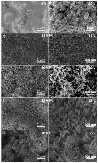
Figure 2.
FE-SEM images of morphology formed at the Cu surface during copper anodizing in 0.01 M NaHCO3 at 5 (a), 10 (b), 15 (c,d), 20 (e,f), 25 (g,h) and 30 V (i,j).
Greater magnifications show that the formed nanowires are densely packed, which makes them promising morphology for all the applications, where high surface area is demanded, i.e., catalysis (Figure 2c–j). For samples prepared at 25 and 30 V FE-SEM imaging showed that the nanowires tend to form bundles (Figure 2g–j).
Additionally, observation of numerous random areas of the samples revealed that the tensions on the surface of the growing anodic nanostructures are so high that the nanowires form various ridges (Figure 3a,b), peaks (Figure 3c) and clusters (Figure 3d). Therefore, such high stresses would rather ease partial dissolution or detachment of the grown oxide. What is even more interesting, certain random zones of the oxidized sample with bimodal distribution of nanowires were found (Figure 3e,f).
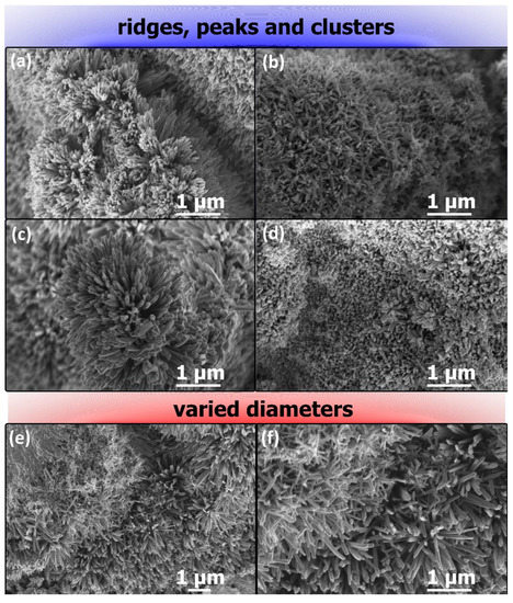
Figure 3.
FE-SEM images of nanostructures formed by copper anodizing in 0.01 M NaHCO3 at 25 (a), 30 (b), 35 (c) and 40 V (d) revealing formation of curved surfaces covered by nanostructures as well as images of nanostructures formed by copper anodizing in 0.01 M NaHCO3 at 25 V, showing two populations of nanowires with various diameters (e,f).
In Figure 3e,f it is apparent that there is a visible boundary between two populations of the nanowires. This can be easily explained by the discussed earlier partial and local delamination of the formed copper oxides/hydroxide, which lead to disruption of the nanowire growth in this section. As the self-healing of this section progresses, new, visibly thinner, nanowires are formed. As a result, in the FE-SEM images, sections with thicker, “older” and sections with thinner, “younger” populations of nanostructures can be distinguished. Nanowires created after partial detachment are thinner due to shorter growth time.
The findings from microscopic observations are in line with quantitative image analysis of the grown oxides (Figure 4).
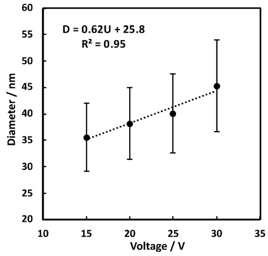
Figure 4.
Dependency of the applied anodizing voltage on the average diameter of the grown nanowires.
Diameter of the nanostructures grows with voltage linearly up to 30 V (Figure 4, Figures S3 and Figure S5). The diameter increases with applied voltage in a range of 15 V (35 ± 6 nm) to 30 V (45 ± 9 nm). At voltage higher than the 30 V average diameter of nanowires decreases (Figure 4 and Figure S3) due to detachment and regrowth phenomena. Simultaneously, for samples prepared at 35 and 40 V, the current density transients show strong oscillations, which confirms occurrence of numerous consecutive detachment-regrowth cycles Presence of both original and regrown nanowires in samples prepared at higher voltage lowers the average nanowire diameter as compared to nanowires in samples anodized at lower voltages.
The influence of applied voltage (15–30 V) on diameter of formed nanowires has been previously reported in two-electrode anodizing setup [33]. It confirms the previous findings on mechanism of copper-derived nanostructures growth during anodizing [33,34], where detachment and redeposition affect diameter of formed nanowires.
Both in the current work and in previous reports on hard anodizing of copper in potassium carbonate [33], the distribution of standard deviations of the average diameters were found to be very wide.
3.3. Crystallinity
X-ray diffraction patterns are presented in Figure 5.
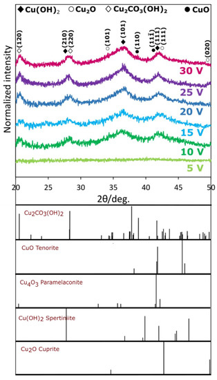
Figure 5.
X-ray diffraction patterns of materials formed by copper anodizing in 0.01 M NaHCO3 at 5–30 V with relevant theoretical patterns calculated for wavelength 1.789010 Å.
It is apparent that for samples anodized at 5 V no crystalline structures were formed. This is in line with FE-SEM observations, where no actual nanostructures were revealed (see Figure 2a). In other cases, also at the highest voltages (35–40 V; see—Figure S5) reflexes originating from monoclinic tenorite (CuO) and cubic cuprite (Cu2O) were found, confirming suggested mechanisms of formation. What is quite uncommon, three reflexes originating from Cu(OH)2 were found in the XRD pattern. Despite the reflexes have low intensity and width, the most distinct ones originate from Cu(OH)2. There are literature reports in which Cu(OH)2 is also found to be crystalline. However, there are numerous cases when only oxides (Cu2O and CuO) were formed by anodizing and passivation in NaOH [38]. On the other hand, according to Zhang and Wang, nanostructures formed by anodizing in NaOH consisted of crystalline Cu(OH)2 and reflexes from tenorite appeared after calcination, i.e., after thermal Cu(OH)2 decomposition into CuO and water [39]. So already at this point, the reported data were found to be unequivocal. Similarly, contradictory data were reported for copper electrochemical oxidation in KOH. For example Wu et al. [40] and Cheng et al. [12] obtained nanostructures that were made of crystalline Cu(OH)2 using galvanostatic passivation in 2 M KOH at 1.5 mA·cm−2. In order to obtain any reflexes from CuO, the samples were annealed for 3 h at 150 °C or 200 °C [40]. On the contrary, Xiao et al. reported formation of Cu2O and CuO, in 0.5–2.0 M KOH at 0.5–4.0 mA·cm−2, as the only crystalline phases [11].
The most probable explanation of the contradictory data is also given in the Figure 5—reflexes from certain phases tend to overlap when are of low intensity and width. For example at ca. 2 theta equal to 43° there are three neighboring reflexes from Cu2O, CuO and Cu(OH)2 that may obscure correct interpretation. Nevertheless, other reflexes confirm the presence of crystalline Cu(OH)2. Furthermore, at certain operating conditions, the nanostructures might grow in a form of a core-shell—oxide core is coated with hydroxide shell that is as thick as the extend of Cu2+ redeposition from the electrolyte. Therefore, at specific experimental conditions (i.e., type of electrolyte, cell assembly, voltage, temperature, electrolyte additives) redeposition of Cu2+ from electrolyte bulk and subsequent Cu(OH)2 formation might be favored, while at other sets of operating conditions, redeposition might be hindered or even blocked.
It is worth noting that in the XRD pattern there are reflexes from malachite, Cu2CO3(OH)2, originating from its two crystallographic planes: (120) at (220). The only reliable explanation of the malachite presence in the samples is electrolyte anions incorporation into the growing anodic coating. This is also in line with our previous findings for copper anodizing in K2CO3 [33]. The presence of carbonates in the anodic coating on the copper were also detected using XPS when copper was anodized in Na2CO3 [28]. It is worth to emphasize that incorporation of anions into anodic oxides, e.g., anodic alumina, is commonly observed. [41]. Due to the anions’ incorporation i.e., in current research also malachite was formed. Generally, when metals like Al or Ti are anodized, the formed oxides as well as the incorporated anions form amorphous products. In the case of copper anodizing, crystalline products are formed, due to more complex mechanism of growth that involves redeposition.
4. Conclusions
Copper anodizing in 0.01 M NaHCO3 leads to nanostructures formation at applied voltage higher than 15 V. The copper-derived nanowires growth mechanism is jet to be thoroughly understood, however the conducted research can be concluded in the following bullet points, which provide some additional insight:
- For greater applied voltages (from 25 V), the current transients are oscillating, which might indicate partial delamination of the grown oxide coatings and its subsequent regeneration.
- The obtained nanowires form bundles and ridges, assumingly due to the internal stresses during anodic oxide growth.
- Consecutive delamination-regrowth cycles occur during anodizing, leading to broad size distribution of grown nanowires.
- Copper anodizing in 0.01 M NaHCO3 results in formation of commonly known crystalline Cu2O and CuO, as well as crystalline Cu(OH)2.
- Crystalline malachite, Cu2CO3(OH)2, was formed due to anions incorporation into anodic coating.
Supplementary Materials
Supporting information file with data for sample anodized at 35 and 40 V is available. The following are available online at https://www.mdpi.com/article/10.3390/cryst11060624/s1, Figure S1. Current density transients of copper anodizing in 0.01 M NaHCO3 registered for 30, 35 and 40 V. Figure S2. Photographs of samples after 2-h-long anodizing in 0.01 M NaHCO3 at various voltages. Figure S3. FE-SEM images of nanostructures formed by copper anodizing in 0.01 M NaHCO3 at 35 (a) and 40 V (b). Figure S4. FE-SEM images of nanostructures formed by copper anodizing in 0.01 M NaHCO3 at 35 (a) and 40 V (b). Figure S5. Xray diffraction patterns of CuOx formed by copper anodizing in 0.01 M NaHCO3 at 30, 35 and 40 V.
Author Contributions
D.G.: samples preparation (MUT), XRD experiments, discussion, writing, editing, funds acquiring; A.B.: discussion, writing, editing; M.R.A.: samples preparation (LU), discussion; K.-K.W.: samples preparation (LU), discussion; W.Z.M.: funds acquiring (LU), supervision, writing, discussion; W.J.S.: Conceptualization, FE-SEM imaging, funds acquiring (MUT), supervision, writing. All authors have read and agreed to the published version of the manuscript.
Funding
This research was funded by Polish Returns 2019 Project granted from Polish National Agency for Academic Exchange (agreement no. PPN/PPO/2019/1/ 00003 /U/0001) and National Science Centre, Poland (NCN-MINIATURA4 DEC- 2020/04/X/ST5/00383). This publication was financially supported by statutory research funds of the Department of Functional Materials and Hydrogen Technology, Military University of Technology, Warsaw. Poland.
Data Availability Statement
Rough data are available on request from corresponding Authors.
Acknowledgments
M.R.A. acknowledge sponsorship from the King Khalid University. M.R.A., K.-K.W. and W.Z.M. cordially acknowledge generous support provided by the Loewy Institute at Lehigh University.
Conflicts of Interest
The authors declare no conflict of interest.
References
- Giziński, D.; Brudzisz, A.; Santos, J.S.; Trivinho-Strixino, F.; Stępniowski, W.J.; Czujko, T. Nanostructured anodic copper oxides as catalysts in electrochemical and photoelectrochemical reactions. Catalysts 2020, 10, 1338. [Google Scholar] [CrossRef]
- Xie, J.F.; Huang, Y.X.; Li, W.W.; Song, X.N.; Xiong, L.; Yu, H.Q. Efficient electrochemical CO2 reduction on a unique chrysanthemum-like Cu nanoflower electrode and direct observation of carbon deposite. Electrochim. Acta 2014, 139, 137–144. [Google Scholar] [CrossRef]
- Mandal, L.; Yang, K.R.; Motapothula, M.R.; Ren, D.; Lobaccaro, P.; Patra, A.; Sherburne, M.; Batista, V.S.; Yeo, B.S.; Ager, J.W.; et al. Investigating the role of copper oxide in electrochemical CO2 reduction in real time. ACS Appl. Mater. Interfaces 2018, 10, 8574–8584. [Google Scholar] [CrossRef]
- Li, J.; Kuang, Y.; Meng, Y.; Tian, X.; Hung, W.-H.; Zhang, X.; Li, A.; Xu, M.; Zhou, W.; Ku, H.-S.; et al. Electroreduction of CO2 to formate on a copper-based electrocatalyst at high pressures with high energy conversion efficiency. J. Am. Chem. Soc. 2020, 142, 7276–7282. [Google Scholar] [CrossRef]
- John, S.; Roy, S.C. CuO/Cu2O nanoflake/nanowire heterostructure photocathode with enhanced surface area for photoelectrochemical solar energy conversion. Appl. Surf. Sci. 2020, 509, 144703. [Google Scholar] [CrossRef]
- Ratynski, M.; Hamankiewicz, B.; Krajewski, M.; Boczar, M.; Ziolkowska, D.; Czerwinski, A. Single step, electrochemical preparation of copper-based positive electrode for lithium primary cells. Materials 2018, 11, 2126. [Google Scholar] [CrossRef] [PubMed]
- Wang, Z.; Zhang, Y.; Xiong, H.; Qin, C.; Zhao, W.; Liu, X. Yucca fern shaped CuO nanowires on Cu foam for remitting capacity fading of Li-ion battery anodes. Sci. Rep. 2018, 8, 6530. [Google Scholar] [CrossRef] [PubMed]
- Li, M.; Li, Y.; Zhang, Q.; Qin, C.; Zhao, W.; Wang, Z.; Inoue, A. Ultrafine Cu2O/CuO nanosheet arrays integrated with NPC/BMG composite rod for photocatalytic degradation. Appl. Surf. Sci. 2019, 483, 285–293. [Google Scholar] [CrossRef]
- Anantharaj, S.; Sugime, H.; Noda, S. Ultrafast growth of Cu(OH)2–CuO nanoneedle array on Cu foil for methanol oxidation electrocatalysis. ACS Appl. Mater. Interfaces 2020, 12, 27327–27338. [Google Scholar] [CrossRef] [PubMed]
- Anantharaj, S.; Sugime, H.; Yamaoka, S.; Noda, S. Pushing the limits of rapid anodic growth of CuO/Cu(OH)2 nanoneedles on Cu for the methanol oxidation reaction: Anodization pH Is the game change. ACS Appl. Energy Mater. 2021, 4, 899–912. [Google Scholar] [CrossRef]
- Xiao, F.; Yuan, S.; Liang, B.; Li, G.; Pehkonen, S.O.; Zhang, T.J. Superhydrophobic CuO nanoneedle-covered copper surfaces for anticorrosion. J. Mater. Chem. A 2015, 3, 4374–4388. [Google Scholar] [CrossRef]
- Cheng, Z.; Ming, D.; Fu, K.; Zhang, N.; Sun, K. pH-controllable water permeation through a nanostructured copper mesh film. ACS Appl. Mater. Interfaces 2012, 4, 5826–5832. [Google Scholar] [CrossRef]
- Scuderi, V.; Amiard, G.; Boninelli, S.; Scalese, S.; Miritello, M.; Sberna, P.M.; Impellizzeri, G.; Privitera, V. Photocatalytic activity of CuO and Cu2O nanowires. Mater. Sci. Semicond. Process. 2016, 42, 89–93. [Google Scholar] [CrossRef]
- Hajimammadov, R.; Bykov, A.; Popov, A.; Juhasz, K.L.; Lorite, G.S.; Kukovecz, A.; Huuhtanen, M.; Kordas, K. Random networks of core-shell-like Cu-Cu2O/CuO nanowires as surface plasmon resonance-enhanced sensors. Sci. Rep. 2018, 8, 4708. [Google Scholar] [CrossRef]
- Sonia, S.; Poongodi, S.; Suresh Kumar, P.; Mangalaraj, D.; Ponpandian, N.; Viswanathan, C. Hydrothermal synthesis of highly stable CuO nanostructures for efficient photocatalytic degradation of organic dyes. Mater. Sci. Semicond. Process. 2015, 30, 585–591. [Google Scholar] [CrossRef]
- Dagher, S.; Halik, Y.; Ayesh, A.I.; Tit, N. Synthesis and optical properties of colloidal CuO nanoparticles. J. Lumin. 2014, 15, 149–154. [Google Scholar] [CrossRef]
- Zhang, X.; Wang, G.; Liu, X.; Wu, J.; Li, M.; Gu, J.; Liu, H.; Fang, B. Different CuO nanostructures: Synthesis, characterization, and applications for glucose sensors. J. Phys. Chem. C 2008, 112, 16845–16849. [Google Scholar] [CrossRef]
- Mosleh, S.; Rahimi, M.R.; Ghaedi, M.; Dashtian, K.; Hajati, S. Sonochemical-assisted synthesis of CuO/Cu2O/Cu nanoparticles as efficient photocatalyst for simultaneous degradation of pollutant dyes in rotating packed bed reactor: LED illumination and central composite design optimization. Ultrason. Sonochem. 2018, 40, 601–610. [Google Scholar] [CrossRef] [PubMed]
- Sahai, A.; Goswami, N.; Kaushik, S.D.; Tripathi, S. Cu/Cu2O/CuO nanoparticles: Novel synthesis by exploding wire technique and extensive characterization. Appl. Surf. Sci. 2016, 390, 974–983. [Google Scholar] [CrossRef]
- Stepniowski, W.J.; Misiolek, W.Z. Review of Fabrication Methods, Physical properties, and applications of nanostructured copper oxides formed via electrochemical oxidation. Nanomaterials 2018, 8, 379. [Google Scholar] [CrossRef]
- Sulka, G.D.; Brzózka, A.; Zaraska, L.; Wierzbicka, E.; Brudzisz, A. AAO templates with different patterns and channel shapes. In Submicron Porous Materials, 1st ed.; Bettotti, P., Ed.; Springer International Publishing: New York, NY, USA, 2017; pp. 107–156. [Google Scholar] [CrossRef]
- Zaraska, L.; Brudzisz, A.; Wierzbicka, E.; Sulka, G.D. The effect of electrolyte change on the morphology and degree of nanopore order of porous alumina formed by two-step anodization. Electrochim. Acta 2016, 198, 259–267. [Google Scholar] [CrossRef]
- Iwai, M.; Kikuchi, T.; Suzuki, R.O.; Natsui, S. Electrochemical and morphological characterization of porous alumina formed by galvanostatic anodizing in etidronic acid. Electrochim. Acta 2019, 320, 134606. [Google Scholar] [CrossRef]
- Iwai, M.; Kikuchi, T.; Suzuki, R.O. High-speed galvanostatic anodizing without oxide burning using a nanodimpled aluminum surface for nanoporous alumina fabrication. Appl. Surf. Sci. 2021, 537, 147852. [Google Scholar] [CrossRef]
- Simon, A.P.; Santos, V.A.Q.; Rodrigues, A.; Santos, J.S.; Trivinho-Strixino, F.; Pereira, B.L.; Lepienski, C.M.; Sikora, M.D.S. Enhancement of mechanical properties and wettability of TiO2NT arrays formed in simulated body fluid-based electrolyte. Adv. Eng. Mater. 2019, 21, 1900813. [Google Scholar] [CrossRef]
- Simon, A.P.; Ferreira, C.H.; Rodrigues, A.; Santos, J.S.; Strixino, F.T.; Marques, P.T.; Junior, H.E.Z.; Sikora, M.S. TioO2NT as platform for drug release: The effect of film wettability. Orbital 2019, 11, 361–366. [Google Scholar] [CrossRef]
- Choi, Y.W.; Kim, S.; Seong, M.; Yoo, H.; Choi, J. NH4-doped anodic WO3 prepared through anodization and subsequent NH4OH treatment for water splitting. Appl. Surf. Sci. 2015, 324, 414–418. [Google Scholar] [CrossRef]
- Stępniowski, W.J.; Paliwoda, D.; Abrahami, S.T.; Michalska-Domańska, M.; Landskron, K.; Buijnsters, J.G.; Mol, J.M.C.; Terryn, H.; Misiolek, W.Z. Nanorods grown by copper anodizing in sodium carbonate. J. Electroanal. Chem. 2020, 857, 113628. [Google Scholar] [CrossRef]
- Oyarzún Jerez, D.P.; López Teijelo, M.; Ramos Cervantes, W.; Linarez Pérez, O.E.; Sánchez, J.; Pizarro, G.C.; Acosta, G.; Flores, M.; Arratia-Perez, R. Nanostructuring of anodic copper oxides in fluoride-containing ethylene glycol media. J. Electroanal. Chem. 2017, 807, 181–186. [Google Scholar] [CrossRef]
- Batista-Grau, P.; Fernández-Domene, R.M.; .Sánchez-Tovar, R.; García-Antón, J. Control on the morphology and photoelectrocatalytic properties of ZnO nanostructures by simple anodization varying electrolyte composition. J. Electroanal. Chem. 2021, 880, 114933. [Google Scholar] [CrossRef]
- Wierzbicka, E.; Syrek, K.; Mączka, K.; Sulka, G.D. Photocatalytic decolorization of methyl red on nanoporous anodic ZrO2 of different crystal structures. Crystals 2021, 11, 215. [Google Scholar] [CrossRef]
- Zhang, Z.; Zhong, C.; Liu, L.; Teng, X.; Wu, Y.; Hu, W. Electrochemically prepared cuprous oxide film for photo-catalytic oxygen evolution from water oxidation under visible light. Sol. Energy Mater. Sol. Cells 2015, 132, 275–281. [Google Scholar] [CrossRef]
- Stępniowski, W.J.; Paliwoda, D.; Chen, Z.; Landskron, K.; Misiołek, W.Z. Hard anodization of copper in potassium carbonate aqueous solution. Mater. Lett. 2019, 252, 182–185. [Google Scholar] [CrossRef]
- Stępniowski, W.J.; Wang, K.-K.; Chandrasekar, S.; Paliwoda, D.; Nowak-Stępniowska, A.; Misiolek, W.Z. The impact of ethylenediaminetetraacetic acid (EDTA) additive on anodization of copper in KHCO3–hindering Cu2+ re-deposition by EDTA influences morphology and composition of the nanostructures. J. Electroanal. Chem. 2020, 871, 114245. [Google Scholar] [CrossRef]
- Stępniowski, W.J.; Misiolek, W.Z. The influence of electrolyte usage on the growth of nanostructured anodic films on copper in sodium carbonate aqueous solution. J. Electroanal. Chem. 2020, 871, 113491. [Google Scholar] [CrossRef]
- Giri, S.D.; Sarkar, A. Electrochemical study of bulk and monolayer copper in alkaline solution. J. Electrochem. Soc. 2016, 163, H252–H259. [Google Scholar] [CrossRef]
- Stępniowski, W.J.; Yoo, H.; Choi, J.; Norek, M.; Jóźwik, P.; Misiolek, W.Z. Fabrication and characterization of oxide nano-needles formed by copper passivation in sodium hydroxide solution. Thin Solid Film. 2019, 671, 111–119. [Google Scholar] [CrossRef]
- Stępniowski, W.J.; Yoo, H.; Choi, J.; Chilimoniuk, P.; Karczewski, K.; Czujko, T. Investigation of oxide nanowires growth on copper via passivation in NaOH aqueous solution. Surf. Interfaces 2019, 14, 15–18. [Google Scholar] [CrossRef]
- Zhang, Z.; Wang, P. Highly stable copper oxide composite as an effective photocathode for water splitting via a facile electrochemical synthesis strategy. J. Mater. Chem. 2012, 22, 2456–2464. [Google Scholar] [CrossRef]
- Wu, X.; Bai, H.; Zhang, J.; Chen, F.; Shi, G. Copper hydroxide nanoneedle and nanotube arrays fabricated by anodization of copper. J. Phys. Chem. B 2005, 109, 22836–22842. [Google Scholar] [CrossRef] [PubMed]
- Le Coz, F.; Arurault, L.; Datas, L. Chemical analysis of a single basic cell of porous anodic aluminium oxide templates. Mater. Charact. 2010, 61, 283–288. [Google Scholar] [CrossRef]


Publisher’s Note: MDPI stays neutral with regard to jurisdictional claims in published maps and institutional affiliations. |
© 2021 by the authors. Licensee MDPI, Basel, Switzerland. This article is an open access article distributed under the terms and conditions of the Creative Commons Attribution (CC BY) license (https://creativecommons.org/licenses/by/4.0/).