1. Introduction
The reliability of soldered interconnections of solar PV modules and other electronic devices is usually assessed using accelerated thermal cycling tests. The control and acceleration parameters that are utilized in thermal cycling tests include dwell times, ramp rates, maximum and minimum ramp temperatures, mean temperature, and cycle time.
Figure 1 shows the relationships between the thermal cycle parameters.
Bath et al., Sharma and Dasgupta [
1,
2] in their respective studies compared dwell times of 10 min to over 30 min. Studies on relatively shorter dwell times and dwell time intervals have also been carried out by [
3,
4]. Clech [
5] proposed an optimum dwell time of 10 min for ball grid array (BGA) assemblies, based on the highest damage rate. A dwell time of 8–10 min at the highest ramp has been recommended by [
6]. The researchers in [
6] further observed that, with dwell times beyond 20 min, the effect on the acceleration factor becomes insignificant since the induced stresses tend to stabilize. Several related studies [
7,
8,
9] however, reported a decrease in a lifetime with increasing dwell time. Xuejun et al. [
7], in their study on the effects of dwell time and ramp rates on lead-free solder joints in flip-chip ball grid array (FCBGA) packages, reported a decrease in fatigue life with an increase in dwell time from 15 to 30 min, and up until 90 min. The results from [
8] show a strong dependency of dwell time on the initiation of failures. Furthermore, [
8] observed that longer dwell times lead to earlier failures as compared with shorter dwell times. Manock et al. [
9] compared 10, 30, and 60 min dwells with 10-min ramps between (0 °C–100 °C) temperature boundaries. Their results show a decrease in a characteristic lifetime in cycles to failure with an increase in dwell time. Several studies have reported conflicting outcomes on the effects of ramp rate on fatigue life of solder joints, but a significant majority [
5,
10,
11,
12,
13] agree that the number of cycles to failure decreases with an increase in ramp rate. For instance, [
12] reported in their findings that a fewer number of cycles to failure occur under thermal shock compared with temperature cycling conditions. Ghaffarian [
11] observed that (10 to 15 °C/min) thermal shock conditions will produce fewer cycles to failure than temperature cycling conditions of (2 to 5 °C/min). Qi, Y., et al. [
13] reported that (95 °C/min) caused more damage than a slower ramp rate of (14 °C/min). The reported differences in cycles to failure are explained by the resulting large change in creep strain energy density per cycle at faster ramp rates.
Bouarroudj et al., and Schubert et al. [
14,
15] reported in their respective studies that test conditions with higher mean temperature lead to significantly shorter lifetimes than test conditions with lower mean temperature. The observed differences in the reported lifetime of solder joints relate to the impact of temperature on the mechanical properties of solder. The research reports that the mean temperature influences the width and height of the stress-strain hysteresis loop produced in the thermal cycling of the solder interconnection. Clech [
5] studied the mean temperature effects of lead-free and tin-lead assemblies and suggested that a minimum lifetime for Sn-Ag-Cu solder interconnection exists when the mean temperature of a thermal cycle profile falls in the range of about 50 °C to 65 °C. The authors [
16,
17] have all suggested that at a lower dwell temperature, the dwell phase is insensitive to duration since there is a minimal amount of accumulated visco-plastic strain. Syed [
18] in estimating acceleration factors for lead-free solders, however, reported that dwell time at lower temperature contributes significantly to failure mechanism when accumulated creep strain is used as the damage indicator in thermal cycling. Syed also observed that high-temperature dwell is the lowest contributor to accumulated creep strain and, therefore, placing too much emphasis on high-temperature dwell could be misleading.
In general, the standard approach for predicting solder joint reliability under a complex temperature profile is to segment it into single or normal profiles and then combine their damage results. Using a numerical approach Pei et al. [
19] conducted a series of numerical simulations to investigate the impact of field conditions on the solder joint fatigue life of an FCBGA packaging. According to the simulation findings, SnPb and SnAgCu solders respond differently in terms of dwell time and mini-cycles. Yang et al. [
20] used a modified linear damage superposition approach to predict the life of solder joints. The authors discovered that solder joint life can be divided into three regions: the first is affected by creep damage, the second by cumulative loading damage, and the third by fatigue damage. According to their findings, the authors concluded that under constant temperature, fatigue damage increases with vibration amplitude, while creep damage increases and then decreases until it eventually stabilizes. Pang et al. [
21] created a vibration fatigue evaluation and inspection technique for predicting the life of solder joints in flip chip on board (FCOB) assemblies using Miner’s rule. The investigators in [
21] accomplished this by evaluating the dynamic characterizations of the FCOBs in vibration tests using an accelerometer and a high-speed camera and found that as the sinusoidal vibration acceleration input increases, the solder joint fatigue life decreases rapidly. Chai et al. [
22] used Engelmair’s model to predict the solder interconnect life expectancy under a dynamic field thermal cycle by segmenting the complex temperature cycle into several basic temperature cycles. Following that, the authors superimposed the damage of the segmented cycles and estimated the existence of solders Sn
62Pb36Ag2, Sn96.5Ag3Cu0.5, and SN100C under the complex temperature cycle. Though the life prediction results of the recommended segmenting scheme were the nearest to their test results, a shift in temperature cycle profile would necessitate a new cycle segmentation process. According to other research findings in [
23,
24], the linear accumulation law does not apply to the majority of dynamic loading conditions. Chen et al. [
25] on the other hand, developed a non-linear damage accumulation rule for solder joint life prediction under a combined profile of two standard temperature cycles based on both damage curve theory and fatigue crack propagation theory. The damage accumulation rule considered both sequential and superimposed effects that resulted in a very simple non-linear damage rule. The authors concluded that the equivalent damage under both segmented standard temperature cycles can be calculated with the damage curve and summarized to achieve the accumulation rule. It is important to note that all the above studies involved different materials and packages, such as printed circuit boards (PCB), insulated gate bipolar transistors (IGBT), and ball grid arrays (BGA). The results of investigations into the effect of ramp rates, dwell times, and temperature gradients on solar PV cell interconnections are scarcely available.
In solar PV cells, the solder interconnection provides mechanical strength to the PV module assembly, as well as electrical path. As a result, increased strain energy accumulation due to fatigue and creep damage will lead to crack initiation and growth. This will lead to loss of electrical contact emanating from increased series resistance and decreased shunt resistance of the solar cell. In this study, accumulated creep energy density (ACED) will be used to assess the life of the cell interconnection during the thermal cycling process. In the thermo-mechanical analysis, creep strain energy density offers a more robust damage indicator in the solder joint as it is based on the deformation that is internally stored throughout the volume of the joint during thermal loading. Thus, the creep strain energy density captures the entire deformation in the joint. Furthermore, the response of accumulated creep energy density as a life prediction parameter provides the advantage of capturing the effect of low temperature dwell better than the accumulated creep strain. In practice, the change in ACED averaged over the volume of solder is used for predicting the cycles of failure. The change in ACED (∆Wacc) will be used to predict the damage in the soldered c-Si PV cell interconnection.
Theory
The Garofalo-Arrhenius model [
26,
27,
28] using accumulated creep strains and dissipated strain energy density which involves exponential dependence on temperature and a hyperbolic sine dependence on high stress, is widely accepted for the characterization of solder alloys. This model is used in this study to formulate the creep response of the solders and IMCs.
In this study, instead of using the usual definition of fatigue, cyclic loading is regarded as a specific case of creep due to the sequence of loading that is repeated cyclically to produce the life prediction model parameters. This is done by using two equations.
The Monkman-Grant equation for creep rupture, as given in Equation (1), states that the time to rupture,
, is inversely related to the steady-state creep strain rate,
, during a test.
The constant
gives the “creep ductility” or the strain at the onset of failure. The above equation assumes constant stress during the creep test. In the situation of variable stresses repeated cyclically, as shown in this study, an estimate of rupture time (or cycles to failure) can be evaluated using a special form of time-fraction rule, as shown in Equation (2). The term inside the summation sign bears similarity with the more recognized Palmgren-Miner rule for cyclic damage.
= number of cycles to failure
n = number of steps within a cycle
= time spent at a stress level within a cycle, and
= rupture time for stress level .
Using Monkmann-Grant equality, Equation (2) becomes
where
is the steady-state creep rate for stress level
. Since the numerator term within the summation sign is the creep strain accumulated during a time
, the summation for all steps n within a cycle gives the accumulated creep strain,
, for the whole cycle. Thus, the above equation can be simplified as
where
= Accumulated creep strain per cycle.
, the inverse of creep ductility.
Equation (4) can also be derived using a fracture mechanics approach, as discussed previously by [
29]. It has also been shown by the author [
29] that this equation can easily be converted into an energy density-based life prediction model:
where,
= Creep energy density per cycle
= Accumulated creep energy density per cycle.
The term ∆W
acc (change in accumulated creep energy density) is obtained by computing the average change in creep strain energy density from the finite element analysis (FEA) results and then normalizing with the volume of the solder used in generating the geometric model. Thus:
where
,
are the total accumulated strain energy density in one element at the endpoint and starting point of one thermal cycle, respectively.
,
is the volume of the element at the endpoint and start point of one cycle, respectively, and
is the number of selected elements used. Consequently, the ACED per cycle (
is evaluated as:
where ‘n’ is the number of thermal cycles.
The accumulated creep energy density (ACED) was evaluated using the creep work command NL CRWK in Ansys. Furthermore, the contributions of ramp rates and dwell times to the degradation of soldered interconnections by ACED of a c-Si PV module under field temperature cycling were investigated. Subsequently, damage prediction functions are generated to predict the damage in the interconnections for a given number of thermal cycles.
2. Materials and Methods
In this investigation, geometric models of solar cells interconnected using two different solder formulations, namely, Pb
60Sn
40 and Sn
3.8Ag
0.7Cu as interconnecting materials were used. The Pb
60Sn
40 represents the solder formulation commonly used as interconnecting material in solar cells whereas the Sn
3.8Ag
0.7Cu (Pb-free) solder represents a potential Pb-free alternative. Four geometric models were generated for the study of each type of solder interconnection. Additionally, four temperature load profiles (for the years 2012, 2013, 2014) and test region average (TRA) thermal cycles generated from three-year real-time monitoring of installed PV modules at the test site were used in the study. The methodology for generating these temperature profiles has been extensively discussed and reported in our earlier study [
30]. The material models used for the different laminating materials of the solar cell are summarized in
Table 1.
The generalized Garafalo-Arrhenius model was used in the study of the creep behaviour of the solders. Intermetallic compound (IMC) thickness of 6 µm comprising Cu
3Sn
5 and Ag
3Sn on either side of the solder material were used to completely model the interconnection. The Garofalo-Arrhenius model [
26,
27,
28] using accumulated creep strain and dissipated strain energy density which involves exponential dependence on temperature and a hyperbolic sine dependence on high stress is widely accepted for the characterization of solder alloys.
The flow equation for creep strain rate is given by:
where
,
and T are the scalar creep strain rate, von Mises effective stress and absolute temperature, respectively. The other symbols
represent material-dependent parameters. This model is used in this study to formulate the creep response of the solders and IMCs.
Table 2 lists the various creep parameters used in predicting the thermo-mechanical response of the solders.
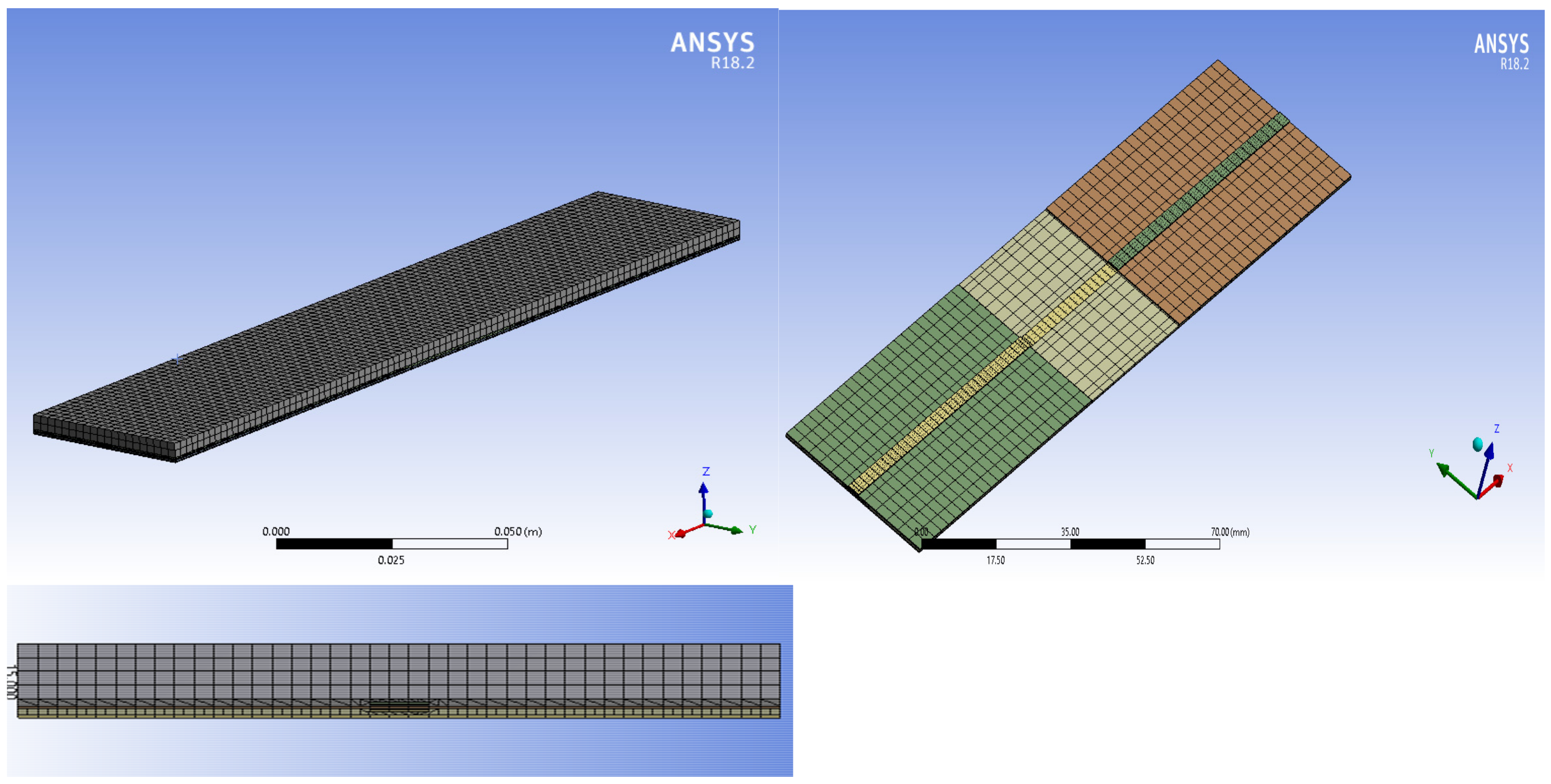
Table 3 lists the various geometric parameters of the PV model. A sliced geometric model (quarter cell) was meshed using the ANSYS mesh creation engine (ANSYS Mesher). This engine discretizes the geometric model enabling equations to be solved at nodal locations. The mesh efficiency and accuracy were improved through refinement and sizing for high solution gradients and fine geometric details.
In this research work, selective mesh adjustment and refinement operations were carried out on the intermetallic compounds (IMC) and solder geometric models. ANSYS mesh refinement settings were applied to the IMC, which is very thin, while a face sizing setting was applied to the solder geometric models, respectively. We applied a system default size of mesh elements with an adaptive size function and a medium relevance centre to the model to generate a mesh with a medium span angle centre and minimum edge length. A total of 195,329 nodes and 49,075 elements constituted the resultant mesh statistics.
Figure 2 shows a meshed geometry of a cell interconnected with an adjacent cell.
Table 4 summarizes the results of temperature cycle profiles generated from in situ thermal cycles as reported by authors in [
30]. The methodology for generating the thermal cycle profiles has been discussed exhaustively in [
30].
Analysis of a Single Thermal Cycle
The c-Si PV cell assemblies were assumed to be at a stress-free state at room temperature of 22 °C, which was approximately equal to the starting temperature of the field thermal cycle loadings. The cell assemblies are also assumed to be at a homogeneous temperature at load steps. The initial stresses in the assemblies, which may be accumulated from reflow soldering processes, are neglected and all contacting surfaces are assumed to be bonded with perfect adhesion.
In a single thermal cycle, the damage accumulation occurs at various load steps defined in the cycle. In this study, a typical daily temperature cycle shown in
Figure 3 has five (5) load steps that can be defined as 1st cold dwell load step, ramp-up load step, hot dwell load step, ramp-down load step, and 2nd cold dwell step. Each of these five load steps generated different damage profiles in the soldered interconnection.
The study focused on evaluating the damage from accumulated creep energy density (ACED) in each load step over twelve (12) thermal cycles. Subsequently, the damage profiles resulting from each category of the thermal load steps were used to generate functions useful in predicting the ACED in the interconnections at a given number of thermal cycles.
3. Results and Discussions
This section presents the results and discussions of the simulation studies.
Section 3.1 deals with the validation of the FEA model by comparing the ACED with results from models developed from experimental studies. The results from this study are also compared with those presented by other researchers.
3.1. FEA Model Validation
The finite element model was validated by comparing the finite element simulation results from the ACED with results from experimental studies. Syed’s [
47] updated life prediction model was used to predict the life of the solder interconnections. Syed’s model is based on creep strain energy density that relates to the deformation stored internally throughout the volume of the solder joint during thermal loading. This model offers a more robust damage indicator in the solder joint since creep strain energy density captures the entire deformation in the joint. In this section, the authors predicted the life of the solder interconnects using the accumulated creep energy density per cycle (
) in Syed’s [
47] updated life prediction model given by:
The cycle time used in this study is 86,400 s (24 h or 1 day). Additionally, [
48] reported that, within a temperature change of about 50 °C, PV modules generally experience one and a half (1.5) thermal cycles per day. Thus, the expected life (
) of interconnects (in years) is evaluated as:
Table 5 presents the results from the evaluation of
,
Nf and
Lyears from Equations (8), (9), and (10), respectively.
From
Table 5, the results from the life prediction study are in close agreement with a study by Guyenot et al. [
48] where the authors estimated the life of PV modules operating per day with an average temperature gradient of about 50 °C as 13,688 cycles (25 years). Besides, the results correlate well with a study by Köhl et al. [
49] in which the authors reported 10,950 cycles in a four-year German project. Furthermore, related studies from Kumar and Sarkan [
50] where the authors recorded a minimum life of 11,497 cycles (21 years) under constant stress accelerated life test on 20 PV modules for stress-related failure closely matches the results from this study. Subsequently, the finite element model was used for the study of creep damage in the soldered interconnections.
3.2. Evaluation of Change in Accumulated Creep Energy Density (ACED) of the Solder Joint
The change in accumulated creep energy density (ACED) is evaluated by computing the difference between the damage accumulated in the solder interconnect from a thermal cycle and the next higher thermal cycle. In this study, we compute the change in the ACED per cycle for the two different types of interconnect solder (Tin lead and lead-free) and present the response of the solder interconnect to creep damage in
Figure 4.
As observed from
Figure 4, the change in accumulated creep energy density reduces sharply in the solder interconnects from the first to the second thermal cycle for all four thermal cycle profiles considered. For the Pb-free solder interconnection, the change in ACED increases steadily after the second thermal cycle for both the 2012 and TRA thermal cycles. However, in the case of the 2013 and 2014 thermal cycles, the change in ACED decreases further but marginally after the second thermal cycle. Similar trends in the change in ACED were observed in the SnPb solder interconnect for 2012, 2013, and 2014 thermal cycles. The TRA thermal cycle, on the other hand, generated an alternating increase and decrease in the change in ACED per cycle in the SnPb solder interconnect. Overall, the change in ACED in Pb-free solder interconnects was observed to be relatively higher than the change in ACED registered in the SnPb solder interconnects for all the four different thermal cycles under study. To study the effect of ramp rates and dwell times on the total damage index, it is important to examine the percentage damage contribution of each of these load steps within the cycle. In the next section, we study the creep damage distribution from the daily thermal cycle profiles.
3.3. Study on Creep Damage Distribution from Thermal Cycles
The distribution of the percentage changes in ACED shows that the ramp-up load step contributes the highest percentage (approximately 50%) of the accumulated damage in the first thermal cycle for all the four different thermal cycle profiles under study (TRA, 2012, 2013, and 2014 thermal cycles). However, the distributions change after the first thermal cycle, showing varied responses from the different thermal cycles and thermal load steps. For every thermal cycle, the combined effect of the ramp-up load step and ramp-down load step accounted for at least 80% of the damage in the two types of solder interconnects.
Another key observation reveals that the damage contribution from the hot dwell load step and cold dwell load step is significantly higher in the SnPb solder interconnects than in the Pb-free interconnects for all the thermal cycles utilized in the study. The subsequent subsections discuss the damage distribution from the four thermal cycles.
3.3.1. ACED Damage Distribution from TRA Thermal Cycle
The damage distribution from the TRA thermal cycle is displayed in
Figure 5. From
Figure 5, the ramp-up load step contributed approximately 36% of creep damage per cycle in both the SnPb and Pb-free solder interconnect during the TRA thermal cycle. Additionally, the creep damage distributions in both interconnections from the TRA thermal cycle shows that the contribution to creep damage from the ramp-down load step remained the highest from the second thermal cycle up to the end of the 12 thermal cycles. The results from the TRA thermal cycle show that, from the second thermal cycle, the contribution of the ramp-down load step to creep damage is slightly higher (approximately 40%) in the Pb-free solder interconnect than the creep damage registered in the SnPb solder interconnect (approximately 37%) from the same ramp-down load step.
The contribution of the 1st cold dwell load steps accounted for the lowest percentage (3%) of the creep damage per cycle. On the other hand, the 2nd cold dwell load step accounted for about 12% in Pb-free solder interconnect and 15% in SnPb solder interconnect, respectively. Additionally, the hot dwell load step accounted for about 5% and 8% of creep damage per cycle in the Pb-free and SnPb interconnects, respectively.
3.3.2. ACED Damage Distribution from 2012 Thermal Cycle
The damage distribution from the 2012 thermal cycle displayed in
Figure 6 showed that, after the first thermal cycle, the damage contribution from the ramp-up load step stabilizes at approximately 35% in the Pb-free interconnect. On the other hand, the damage contribution from the ramp-up load step increases after stabilizing around 30% in the second (2nd) and third (3rd) thermal cycle in the PbSn interconnect. It rises to a peak value of 40% at the fifth (5th) and sixth (6th) thermal cycle. Subsequently, the damage from the ramp-up load step declined from the seventh (7th) thermal cycle and again stabilized at 30% from the eighth (8th) cycle up to the eleventh (11th) thermal cycle.
The ramp-down load step contributed approximately 42% of the damage accumulation per cycle in the Pb-free solder interconnect. The damage within the Pb-free interconnect from the hot dwell load step contributed approximately 8% of the accumulated damage per cycle. The 1st cold dwell step contribution to the damage per cycle remained the lowest (at 2%), while the 2nd cold dwell step accounted for 10% of the damage in the Pb-free solder interconnect. The damage distribution in the PbSn solder interconnect from the 2012 thermal cycling showed that the damage contribution from the ramp-up load step peaked at the 5th and 6th thermal cycles with nearly 40% of the damage contribution. Subsequently, the damage contribution declined to an average value of 30% after the 7th thermal cycle. The 2nd cold dwell step and the hot dwell load step generated significant creep damage in the PbSn solder interconnect after the 6th thermal cycle with 15% and 10% contribution per cycle, respectively.
3.3.3. ACED Damage Distribution from 2013 Thermal Cycle
The damage distribution of ACED from the 2013 thermal cycle displayed in
Figure 7 shows a nearly equal percentage distribution in creep damage for ramp-up (heating) and ramp-down (cooling) load steps in both types of interconnections after the first thermal cycle.
The ACED from the heating and cooling load steps accounted for about 88% of the total accumulated creep damage in the Pb-free solder interconnect. Similarly, the heating and cooling load step show accounted for 78% of the total accumulated damage in the PbSn solder interconnect. The remaining three load steps (1st cold dwell, 2nd cold dwell, and hot dwell) contributed 12% and 22% of the accumulated creep damage in the Pb-free and PbSn solder interconnects, respectively.
3.3.4. ACED Damage Distribution from 2014 Thermal Cycle
The damage distributions from the 2014 thermal cycle shown in
Figure 8 displays similar trends as in the 2013 thermal cycle, with the combined accumulated, creep energy damage from the heating and cooling load step accounting for 90% of the total accumulated creep energy damage in the Pb-free interconnect. A similar damage distribution can be observed in the PbSn interconnect where the heating and cooling load steps accounted for 76% of the total damage.
The damage from hot and cold dwell periods in the SnPb interconnects recorded a significant value of 24%, whereas a relatively lower percentage of 10% was generated in the Pb-free solder. The damage distribution from the four thermal cycles (TRA, 2012, 2013, and 2014) studied shows that the ACED is sensitive to the thermal cycle parameters of dwell time and temperature ramp rate. To quantify the effect of ramp rates and dwell times of the thermal cycle on the damage accumulation, it is imperative to study the damage profiles resulting from both ramp rates and dwell times to generate some functional relationships between them, as well as the total accumulated creep energy density. The next section discusses the damage accumulation profiles from the five thermal load steps.
3.4. Study on Damage Accumulation Profile at Temperature Dwells
3.4.1. ACED Damage profile at Cold Dwell Load Step at the Start of Thermal Cycle
The change in ACED in the soldered interconnects from the cold dwell load steps across the four thermal cycles (2012, 2013, 2014, and TRA) is presented in
Figure 9. The first cold dwell load step in each thermal cycle generated the minimum ACED within the soldered interconnects.
The contribution to damage from the first cold dwell step in each thermal cycle remained insignificant. The damage accumulation profiles in the Pb-free interconnect from 2012, 2014, and TRA thermal cycles exhibited clear similarities across the 12 cold dwell load steps corresponding to the start of each cycle. Generally, they showed a sharper rise in the change in ACED from the end of the first load step up to the end of the 2nd cold dwell load step corresponding to the start of the second thermal cycle. Subsequently, they exhibited a drop in ACED at the third cold dwell load step. After the 3rd cold dwell load step, the changes in ACED from the respective thermal cycle loads assumed polynomial profiles.
The damage profiles in Pb-free solder interconnects from 2014 and TRA thermal cycles trend closely with the damage profile in Pb-free solder interconnects. On the other hand, the damage profile in SnPb and Pb-free interconnects from the 2013 thermal cycle declined further from the 3rd cold dwell load step through to the 5th load step. Furthermore, the damage profile assumed a steady rise from the 5th cold dwell load steps up to the 7th thermal cycle. Subsequently, the damage profiles in both interconnects assumed stagnation from the 7th cold dwell load step to the end of the 11th load step, and finally, the profiles dropped sharply at the end of the 12th cold dwell load step. The damage profile in PbSn interconnect from the 2012 thermal cycle displayed a fluctuating profile up to the 9th cold dwell step. After the 9th cold dwell load step, the profile assumed a steady rise up to the end of the 12th thermal cycle. The results from this study showed that the change in ACED from the cold temperature dwell at the start of each thermal cycle in SnPb interconnects for all four thermal cycling conditions was generally higher than that in Pb-free interconnects.
3.4.2. ACED Damage at Cold Dwell Load Step at the End of Thermal Cycles
The change in ACED profiles during the end of each thermal cycle (cold dwell at the start of the thermal cycle) displayed in
Figure 10 showed similarities to the cold dwell load steps at the start of the thermal cycle.
The distinction observed revealed that, for the cold dwell steps at the end of each cycle, the change in ACED registered a peak value initially at the end of the 1st dwell load step as against the second dwell load step registered in
Figure 9. Additionally, the change in ACED generated per load step during the temperature dwells at the end of the thermal cycles was observed to be relatively higher than that at the start of the thermal cycle (1st cold dwell load step).
3.4.3. ACED Damage Profile at Maximum Temperature Dwell (Hot Dwell Load Step)
The damage profiles depicted in
Figure 11 from maximum temperature dwell (hot dwell load steps) show similar trends except for the profile generated from the 2012 thermal cycle. The damage profiles from the 2012 (SnPb), 2013, 2014, and TRA (SnPb) thermal cycles in
Figure 11 show sharp increases in the change in ACED to peak values at the end of the first (1st) hot dwell load step, followed by a corresponding sharp drop at the end of the 2nd hot dwell load step.
Furthermore, relatively higher amplitudes in the change in ACED were observed for SnPb solder interconnects across all the thermal cycles at the end of the second hot dwell temperature load step. Subsequently, the profiles (from 2013, 2014, and TRA (SnPb) thermal cycles) show approximately linear trends from the third thermal cycle onwards. On the other hand, the damage profiles from the 2012 thermal cycles exhibited non-linearity in the damage profiles for the two types of interconnects after the 2nd hot dwell. The damage profile of TRA (Pb-free) assumed a steady decline from the second hot dwell load step up to the end of the 3rd hot dwell load step, followed by a steady rise up to the end of the 12th thermal cycle. The damage profiles at temperature ramps are discussed in the next subsection.
3.5. Study on ACED Damage Accumulation profile at Temperature Ramps
3.5.1. ACED Damage Profile at Heating (Ramp Up) Load Step
The ramp-up load steps displayed in
Figure 12 generated a relatively higher change in the ACED per cycle within the Pb-free interconnects than in the SnPb interconnects. This is in sharp contrast with the cold dwell load steps where the damage profiles exhibited a relatively higher change in ACED within the SnPb interconnects. Within the Pb-free interconnects, the damage profiles from all four thermal cycles (2012, 2013, 2014, and TRA) exhibited a sharp increase in ACED at the end of the first load step. Subsequently, the damage profiles experience a gradual drop in amplitude for up to the 4th thermal cycle. However, a steady increase in ACED was observed for the TRA and 2012 thermal cycle, while marginal declines were observed for the 2013 and 2014 thermal cycles.
On the other hand, within the SnPb interconnects, the change in ACED per cycle remained constant after a steady rise to the 2nd ramp-up load step across 2013, 2014, and TRA thermal cycles. More so, the damage profile in SnPb solder interconnection from the 2012 thermal cycle appears to trend closely with the profile from the Pb-free interconnect.
3.5.2. ACED Damage Profile at Cooling Ramp Down Load-Step
The damage profiles resulting from the ramp-down Load steps displayed in
Figure 13 show more linearity across the 12 load steps compared with the damage profiles at the ramp-up load steps. The changes in ACED in both Pb-free and SnPb interconnects from 2013 and 2014 thermal cycles show a steady rise up to the 2nd load step. Subsequently, they assume a marginal decline up to the 12th ramp-down load step. The TRA thermal cycle imposed a similar damage profile in the SnPb interconnect. On the other hand, the damage profile in the Pb-free interconnect from the TRA and 2012 thermal cycles showed a sharp rise up to peak values at midway into the 2nd ramp-down load step.
Subsequently, the change in ACED drops at the end of the 2nd ramp down load step, followed by a steady rise up to the end of the 12th thermal cycle from the TRA and 2012 thermal cycles. In the next section, a damage function from the summation of ACED from the various load steps is generated to predict the life of interconnects from ACED damage under thermal cycling.
3.6. Generating Accumulated Creep Damage Function for Solder Joint Life Prediction
In this section, the damage profiles from the change in ACED from the five different load steps in each cycle are predicted as functions of the respective load steps using polynomial and logarithmic functions to approximate the trend lines from data points generated by the FEA results.
Figure 14 and
Figure 15 show plots of change in ACED for the various thermal load steps for the Pb-free solder.
The TRA thermal cycle is used as the representative thermal cycle to generate the functions for the solder joint life prediction.
Figure 14 and
Figure 15 also show the damage profiles together with their respective functions for prediction.
It was also observed that all the damage profiles approximated logarithmic functions at the second dwell and ramp load steps. Beyond the second dwell and ramp load steps, the ACED profiles approximated six-order polynomial functions. The results from the regression analysis show that all the logarithmic functions provided a perfect fit for each data set with a coefficient of determination value of one (R2 = 1). The six-order functions also provided nearly perfect fits to the data sets with (R2=0.9874) being the widest spread.
In general, the trends from the change in ACED profiles can be predicted by a step function as:
where the subscripts
‘ij’ denote the damage corresponding to a particular load step. The following variables can be defined to correspond to the dwell/ramp load steps:
= cold dwell load step at the start of each thermal cycle (1st cold dwell);
= cold dwell load step at the end of each thermal cycle (2nd cold dwell);
= load steps from temperature ramp-ups;
= load steps from temperature ramp-downs;
= load steps from hot dwell;
= change in ACED from 1st cold dwell;
= change in ACED from 2nd cold dwell;
= change in ACED from temperature ramp-ups;
= change in ACED from temperature ramp-downs;
= change in ACED from hot dwells.
3.6.1. ACED Damage Functions for b-free Solder Interconnects
3.6.2. ACED Damage Functions for PbSn Interconnects
Therefore, the ACED over the 12 thermal cycles is written as:
The temperature dwells and ramps occur at equal time steps (time intervals), respectively. Thus, the damage prediction functions can be simplified by representing the load steps for the temperature dwells and ramps with single variables as:
, , and
The prediction functions can be combined and simplified in the following subsections:
3.6.3. ACED Damage in Pb-free Interconnects
3.6.4. ACED Damage in Pb-Sn Interconnects
A further simplification of the damage prediction functions is achieved by substituting the different variables for dwells and ramps with a single variable ‘Ls’ such that:
X = Y = Z= Ls; where L
s is defined as the number of thermal load steps involved in generating ACED damage profile. Thus, the total ACED function over the 12 cycles is given as;
PbSn solder interconnect
The above Equations (29) and (30) are used as damage prediction functions to estimate the ACED per cycle (W
acc) in the solder interconnects for the test region. From Equation (2), the ACED per cycle (W
acc) relation over 12 thermal cycles is evaluated as:
Thus,
is computed by summing up the step functions generated within the limits of the thermal cycle number as:
Table 6 and
Figure 16 present the results from ACED from Ansys FEA simulation and the ACED damage functions generated from the temperature ramp rates, and dwells. From
Figure 16, ACED of 0.13,572 MJ/mm
3 will lead to a complete interconnection break (shunting of the solar cell) in the Pb
60Sn
40 soldered cell interconnect at the test site. This also translates into 12,814 cycles and 23.4 years before failure (
Table 5). On the other hand, ACED of 0.23275 MJ/mm
3 will cause a crack, and, subsequently, an open circuit in the Sn
3.8Ag
0.7Cu (Pb-free) soldered interconnect.
From
Table 6 and
Figure 16, the damage functions predict the ACED values with close approximations to results from the FEA simulation from Ansys. The Pb
60Sn
40 interconnection gives a closer approximation of 0.13242 MJ/mm
3 (2.33% variation) as compared with the Sn
3.8Ag
0.7Cu (Pb-free) interconnection damage of 0.22635 MJ/mm
3 (2.47% variation).
Thus, Equations (25) and (26) can be generated to predict the total damage from ACED in both Pb-free and SnPb interconnects in c-Si photovoltaic cells installed at the test site for the number of thermal cycles used in this study. Subsequently, the expected life (number of cycles to failure) of the soldered interconnect from the estimated thermal cycles can be computed.
3.6.5. Generalized ACED Damage Prediction Functions for Pb60Sn40 and Sn3.8Ag0.7Cu for c-Si PV Modules at Test Site
Equations (32) and (33) can be generalized and used to predict the ACED damage in the soldered interconnections for a given number of thermal cycles at the test site. Thus, for a given number of cycles (n), an equal number of load steps (Ls) for ramps and dwells (Ls = n) can be found.
Thus, in general, the change in ACED for c-Si PV interconnections for the test site for ‘n’ number of thermal cycles is given by:
and
Thus, to predict the number of cycles to failure of soldered interconnections at a test site, the thermal cycle profile of the test site is generated by real-time monitoring. Subsequently, a 12-thermal cycle is generated as a thermal cycle load for the prediction. Finally, a generalized function is derived which is capable of predicting the life of the soldered interconnection for a given number of thermal cycles.
These equations are useful in saving computational space, time, and cost as the FEA simulation from even a fewer number of thermal cycles tends to generate several gigabytes of data, which require substantial computing storage on a hard drive.


