Article

Carrier Dynamics in InGaN/GaN-Based Green LED under Different Excitation Sources

1
Department of Physics, School of Electronic and Information Engineering, Qilu University of Technology (Shandong Academy of Science), Jinan 250353, China
2
International School for Optoelectronic Engineering, Qilu University of Technology (Shandong Academy of Science), Jinan 250353, China
3
College of Physics and Electronics, Shandong Normal University, Jinan 250014, China
*
Authors to whom correspondence should be addressed.
These authors are co-first authors.
Crystals 2021, 11(9), 1061; https://doi.org/10.3390/cryst11091061
Submission received: 1 August 2021 / Revised: 28 August 2021 / Accepted: 30 August 2021 / Published: 2 September 2021

Abstract

:
The excitation power and temperature dependence of the photoluminescence (PL) and electroluminescence (EL) spectra were studied in green InGaN/GaN multiple quantum well (MQW)-based light-emitting diodes (LED). An examination of the PL-325, PL-405, and EL spectra at identical optical or electrical generation rates at room temperature showed that the normalized spectra exhibited different characteristic peaks. In addition, the temperature behavior of the peak energy was S-shaped for the PL-405 spectrum, while it was V-shaped for the EL spectrum. These measurement results demonstrate that the excitation source can affect the carrier dynamics about the generation (injection), transfer, and distribution of carriers.

1. Introduction

In recent years, GaN-based light emitting diodes (LEDs) have been used in an increasing number of applications, including general lighting applications and visible light communications, due to the significant progress achieved in GaN material growth and device manufacturing [1,2,3]. However, GaN-based LEDs and particularly the LEDs emitting at longer wavelengths in the green/yellow spectral range still suffer from unfavorable characteristics such as a high density of defect states, large strain-induced polarization caused by lattice mismatch, and undesirable Auger recombination at high excitation power density [4,5,6]. These unfavorable properties affect carrier dynamics in InGaN/GaN multiple quantum wells (MQWs), which are the basis of the LEDs, thereby reducing the light quantum efficiency. Therefore, understanding the mechanisms of carrier dynamics in InGaN MQWs structures is vital for the further development of InGaN-based optoelectronics devices.
Photoluminescence (PL) and electroluminescence (EL) are basic measurement methods for investigations of optoelectronic semiconductor devices because of their advantages of convenience and high sensitivity. Although both PL and EL result from the recombination of excessive electrons and holes, their carrier dynamics processes are fundamentally different, namely photon injection by optical illumination in PL and current injection from the n- or p-layer in EL. However, to the best of our knowledge, there have been no detailed experimental reports on the comparison of emission mechanisms of PL and EL from 6 to 300 K under the same optical or electrical generation rate [7,8,9,10].
In this study, based on the successful growth of green InGaN/GaN MQWs-based LED on a silicon (Si) substrate, the excitation power and temperature dependence of the PL and EL spectrum were measured. The obtained results revealed the underlying carrier dynamics through the analysis of the emission energy, linewidth, and intensity.

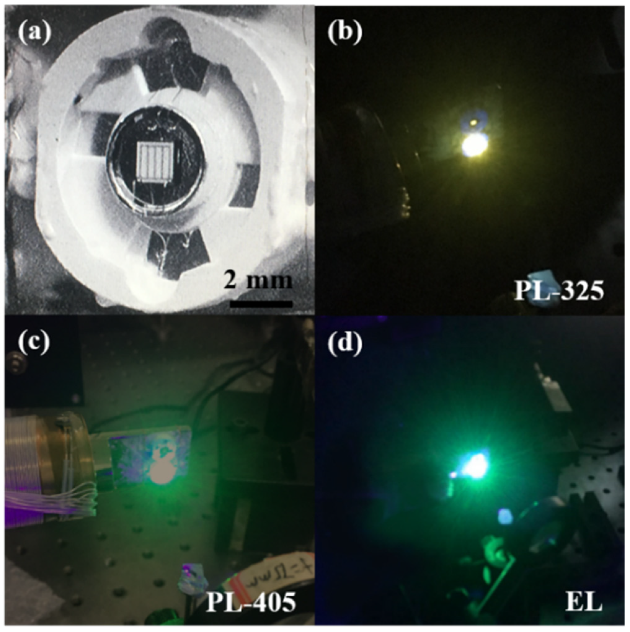
2. Materials and Methods

GaN-based green LEDs were grown on a trenched Si (111) substrate by metalorganic chemical vapor deposition (MOCVD). Trimethylaluminum (TMAl), trimethylgallium (TMGa), trimethylindium (TMIn), ammonia (NH3), and silane (SiH4) were used as the Al, Ga, In, N, and Si precursors, respectively. Prior to growth, thermal annealing was carried out at 1100 °C under hydrogen atmosphere to remove the surface contamination of the substrates. For the GaN-based green LEDs, four pairs of InGaN/GaN MQWs with 2-nm-thick In0.35Ga0.65N wells and 14-nm-thick GaN barriers were grown under N2 ambient following the growth of a 2-µm-thick undoped GaN buffer layer and a 2-µm-thick Si-doped GaN epitaxial layer. The wells and barriers were grown at 770 and 870 °C, respectively. Subsequently, a 20-nm-thick Mg-doped p-AlGaN electron blocking layer (EBL) followed by a 150-nm-thick p-GaN contact layer was grown directly on the last GaN barrier layer of the MQWs. In addition, another two samples with different structures were grown. Sample-N included a 2-µm-thick undoped GaN buffer layer and a 2-µm-thick Si-doped GaN epitaxial layer. Sample-P only included a 150-nm-thick Mg-doped p-GaN contact layer. The growth conditions of the two sample refer to the above LEDs. The electronic concentration of the n-GaN layer was 1 × 1019 cm−3, and the hole concentration of the p-AlGaN EBL and p-GaN contact layer was 1 × 1017 cm−3 and 5 × 1017 cm−3, respectively. The LED chip with the dimensions of approximately 1.16 × 1.16 mm2 was fabricated using a conventional mesa structure method, as shown in Figure 1a.
Figure 1b–d shows luminescent images of the green LED chip under excitation of 325-laser, 405-laser, and current, respectively, measured at room temperature. The chip was mounted on a Cu cold stage in a temperature-variable closed-cycle He cryostat to allow variation of the sample temperature over a wide range from 6 to 300 K. The signals were analyzed using a Jobin-Yvon iHR320 monochromator equipped with a thermoelectrically cooled Synapse CCD detector. For PL measurements, the 325 nm line of a He-Cd laser and the 405 nm line of a semiconductor laser were used as the excitation light source. Meanwhile, for the EL measurements, a Keithley 2400 source meter was used as the excitation current source. The excitation power for the PL-325, PL-405, and EL spectra changed from 0.002 to 20 mW, 0.001 to 100 mW, and 0.001 to 350 mA, respectively.
For clarity, the incident PL excitation power and the EL excitation power were respectively converted to optical and electrical generation rates [9,11,12]. The absorption coefficient is calculated by
α = α 0 ( E E g ) / E g
where α0 is the absorption coefficient at E = 2Eg, E is the laser photon energy, and Eg is the bandgap energy. The absorbance can be expressed as
A = 1 e α l
where l is the effective thickness of light absorption. Finally, the generation rate can be estimated from experimental parameters using
G P L = P l a s e r ( 1 R ) ( 1 e α 0 ( E E g ) / E g l ) A s E l
where Plaser is the laser power, R is the Fresnel reflection at the sample surface, and As is the area of the laser spot. For the PL-325 measurement, all the epitaxial layers are excited by the 325-laser, and the 325-laser power of Plaser = 2 μW (As = 3.55 × 10⁻⁶ cm2) gives a PL-325 generation rate of 1.5 × 1021 cm−3s−1. As comparison, only the InGaN epitaxial layers are excited by the 405-laser during the PL-405 measurement, and the 405-laser power of Plaser = 1 μW (As = 9.29 × 10⁻⁵ cm2) gives a PL-325 generation rate of 1.5 × 1021 cm−3s−1.
Furthermore, the EL generation rate is given by
G E L = I A s e l Q W
where I, e, and lQW are current, elementary charge, and the thickness of the total QWs, respectively. For example, a current of 2.5 μA corresponds to a generation rate of 1.5 × 1021 cm−3s−1.

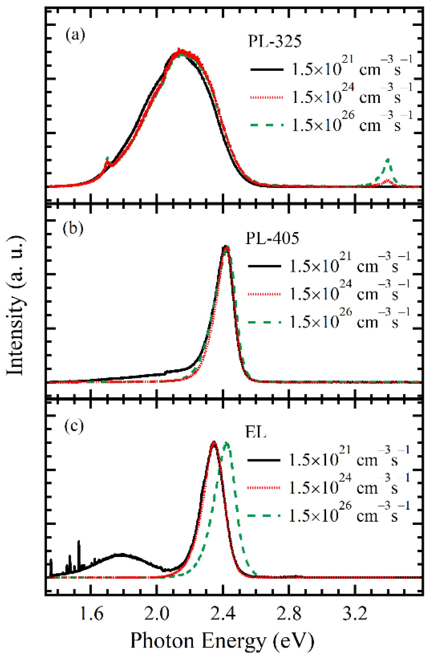
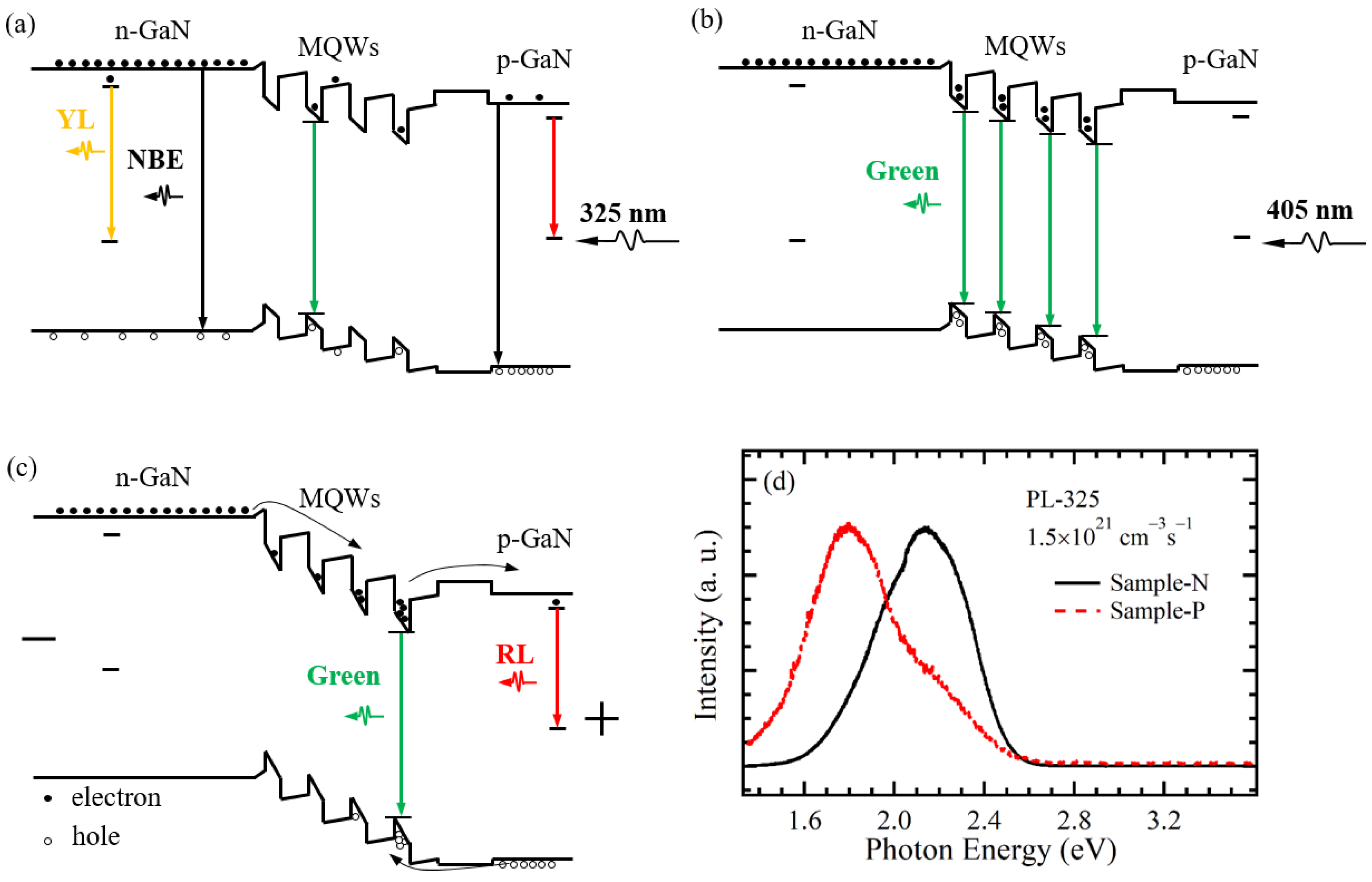
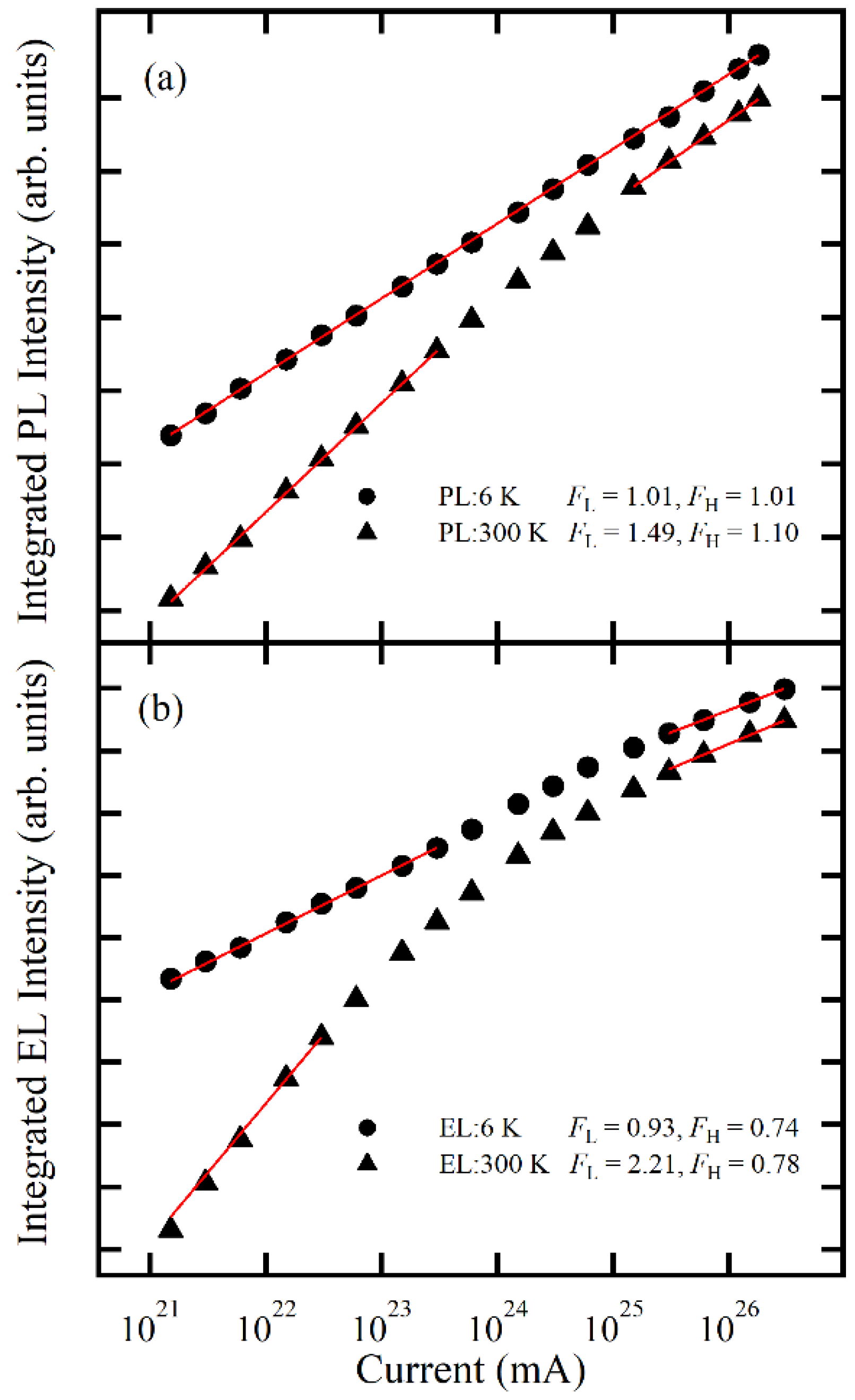
3. Results and Discussion

Figure 2 shows the normalized spectra of the LED chip with excitation power range from 1.5 × 10²¹ to 1.5 × 1026 cm−3s−1 at 300 K measured with different excitation source. As shown in Figure 2a at low excitation power, the PL-325 spectrum was dominated by a very broad yellow luminescence (YL) band at approximately 2.2 eV, which is commonly observed for GaN epitaxial layers and may be ascribed to gallium vacancy (VGa)-related defects [13,14,15]. With the increase in the excitation power to 7.5 × 1026 cm−3s−1, a new emission peak at approximately 3.40 eV appeared on the high energy side of the YL band. This peak originates from the flat-band region of the GaN epitaxial layer and is known as the near-band edge (NBE) emission [16,17,18]. The appearance of NBE with increasing excitation power can be explained as follows. For the excitation power of 1.5 × 1021 cm−3s−1, there are more defect states than free carriers, so that defect-related emission was more likely to occur than the NBE transitions. Therefore, the PL-325 spectrum at low excitation power was dominated by the YL band only. As the excitation power increased to 7.5 × 1026 cm−3s−1, the NBE emission grew faster than the YL band, due to the limited number of defect states [17]. In other words, the NBE to the YL intensity ratio increased. By contrast, as shown in Figure 2b, compared to the PL-325 spectra, the PL-405 spectra at low and high excitation powers were dominated by green emission at approximately 2.41 eV, which is similar to that obtained from the green InGaN/GaN MQWs-based LEDs [19,20]. In addition, a band-tail state was observed on the low-energy side of the PL-405 spectrum at low excitation power. When the current is used as the excitation source, the spectra are still dominated by the green emission. Meanwhile, an unexpected red luminescence (RL) band emission at approximately 1.77 eV appeared, as shown in Figure 2c, and then disappeared with the excitation power increasing from 1.5 × 10²¹ to 7.5 × 1026 cm−3s−1.
To explain the aforementioned spectrum measurement results under the excitation by 325-laser, 405-laser, and current, Figure 3a–c shows energy band diagrams from undoped GaN buffer layer to p-GaN layer, which indicates the possible mechanism of carrier generation (injection), transfer, and distribution in the MQWs structure. Figure 3a shows the energy band diagrams excited by 325-laser for which the photon energy (3.81 eV) was larger than the bandgap energies of the GaN epitaxial layer (3.4 eV) and the InGaN quantum wells. The photo-generated carriers generated by the 325-laser were distributed throughout the entire epitaxial layer from the undoped GaN buffer layer to the p-GaN layer, and almost no transport was observed due to the absence of an external electric field. In addition, a large number of defects such as VGa were present in the GaN epitaxial layer, leading to the occurrence of the YL band observed in PL-325 spectrum, as shown in Figure 2a. However, the green emission associated with the InGaN matrix-related NBE transition was not observed either at low or high excitation power. This can be attributed to the fact that, although the internal quantum efficiency of the InGaN QWs was much higher than that of the GaN epitaxial layer, its total thickness (approximately 8 nm) was too low so that the layer had a negligible effect compared to the effect of the GaN epitaxial layer with a thickness of approximately 5.2 μm. Therefore, green emission was too weak to be observed.
As shown in Figure 3b, for the PL-405 measurements, we employed resonant optical excitation with an excitation wavelength of 405 nm. The photon energy of the 405-laser is greater than the InGaN bandgap energy but is lower than the GaN bandgap energy. Thus, the GaN epitaxial layer was transparent to the photons, and only the InGaN MQWs were excited. This means that the generation and recombination of photo-generated carriers occurred in the InGaN QWs. In addition, since the numbers of the photo-generated carriers in each InGaN well layer excited by the 405-laser were almost equal, the contributions of all InGaN well layers to the PL-405 spectrum were approximately the same [8,9,10]. Therefore, it is clear that the green peak and its band-tail state shown in Figure 2b are derived from the InGaN QWs, rather than from the other epitaxial layers. The deep localized states in the green InGaN/GaN MQWs are the most likely origin of the band-tail state [20,21]. The band-tail state disappeared in the PL-405 spectrum at high excitation power, reflecting the fact that the deep localized states became gradually saturated due to the small density of the deep localized states.
As shown in Figure 3c, in the EL measurements, the electrons were injected into the InGaN well layers from the n-GaN layer, while holes were injected into the InGaN well layers from the p-GaN layer under the action of the external electric field. Electrons and holes tend to be confined within the last QW due to the difficulty of injecting holes from the p-type region into QWs, and the local characteristics of the carrier recombination in the InGaN matrix. The last QW plays a dominant role in the radiative recombination of the MQW active region in the EL measurements [22,23]. In other words, the EL spectrum mainly stems from the contribution of the last QW. Therefore, the green emission in the EL spectrum was observed from the contribution of the last QW, as shown in Figure 2c.
Furthermore, the EL spectrum shown in Figure 2c displayed an RL band at 1.77 eV, as described above. This peak did not originate from the InGaN/GaN MQWs, because no corresponding RL band was observed in the PL-405 spectrum shown in Figure 2b. To further confirm the origin of the RL band, Figure 3d shows normalized spectra of the Sample-N and Sample-P with excitation power of 1.5 × 1021 cm−3s−1 at 300 K under excitation of 325-laser. The spectrum of Sample-P displayed the RL band with a shoulder peak (YL band) on the high-energy side, whereas the spectrum of Sample-N was dominated by the YL band. It means that the RL band can only originate from the Mg-doped p-GaN layer and relate to the Mg impurity, as well as the RL band for the GaN-based green LEDs. Furthermore, as mentioned above, it was difficult for the holes to be injected into the MQWs active region, because of their low concentration and large effective mass, which leads to electron leakage from the last QW into the p-AlGaN EBL and p-GaN contact layer [24,25]. Meanwhile, it was reported that N vacancies (VN) or VN-MgGa are the origin of RL band especially in GaN:Mg films, and the formation energies of VN and VN-MgGa decrease with the lowering Fermi level [17,26,27]. Above all, we strongly suspect that the RL band at low excitation power may originate from the p-GaN contact layer, as shown in Figure 2c. At high excitation power, due to the limited number of VN and VN-MgGa, the RL band grows more slowly than the green emission, despite the stronger electron leakage. The ratio of the green and RL intensities increased, supporting our assignment of the RL band to the VN or VN-MgGa in the p-GaN contact layer. Meanwhile, compared to the PL-405 spectrum, the peak energy of the EL spectrum shows a large blue shift with increasing the excitation power, which is attributed to the larger Coulomb screening of the quantum confined Stark effect (QCSE) in EL spectrum. Besides, the thickness of the AlGaN layer in the GaN-based green LEDs is too thin, resulting in a weak RL intensity, compared with that of YL band. Therefore, the RL band was not observed in the 325-spectrum of the GaN-based green LEDs, as shown in Figure 2a.
To further study the difference of the green emission under 405-laser excitation and the current excitation, Figure 4a shows the temperature-dependence of the PL-405 and EL peak energies for the green LEDs, as obtained by fitting the corresponding spectrum to Gaussian functions. For the PL-405 spectrum, the temperature behavior at 1.5 × 1021 cm−3s−1 is observed to be S-shaped (decrease-increase-decrease) for the peak energy, which was attributed to the potential inhomogeneity and localized character of the carrier recombination due to the slight composition fluctuations in the InGaN matrix [20,21,28]. Upon increasing the excitation power from 1.5 × 10²¹ to 1.5 × 1024, and further to 1.5 × 1026 cm−3s−1, the temperature behavior of the peak energy gradually evolved from a strong S-shaped temperature-dependence into a weak S-shaped relationship, and then finally change to an inverted “V-shaped” temperature dependence, indicating that, upon increasing the excitation power, the carrier localization effect gradually decreased.
By contrast, the temperature behavior of the peak energy for the EL spectrum was “V-shaped” over the temperature range of 6–300 K at the excitation power of 1.5 × 1021 cm−3s−1. In other words, the temperature behavior of the peak energy for the EL spectrum showed a blue shift rather than a red shift at the temperature range from 220 to 300 K, unlike the PL-405 spectrum at the same excitation power. The differences in the behavior of the peak energies with increasing temperature between the PL-405 and EL spectra indicated that the emission process of the EL spectrum was dominated by Coulomb screening in the higher temperature range. In this temperature range, the Mg impurity was continuously ionized, resulting in more holes to be injected into the last QW from the p-AlGaN EBL and the p-GaN contact layer. Therefore, Coulomb screening of free carriers dominated the recombination process of the MQWs, leading to a flattening of the energy band and an increase in the peak energy. However, for the PL-405 spectrum, there was no transport of the photogenerated carriers between the epitaxial layers, and the peak energy became consistent with the Varshni equation in the temperature range from 200 to 300 K. When the excitation power continued to increase from 1.5 × 10²¹ to 1.5 × 1026 cm−3s−1 for the EL spectrum (Figure 4b), the temperature behavior of the peak energy gradually evolved into an inverted V-shape, consistent with the PL-405 spectrum.
Additionally, as shown in Figure 4a, the temperature-dependent curve for the EL spectrum shifted upward by approximately 150–200 meV as the excitation power increased from 1.5 × 10²¹ to 1.5 × 1026 cm−3s−1, while the curve for PL-405 spectrum only shifted upward by approximately 50 meV. This observation can be explained as follows. For the PL-405 spectrum, although the excitation power increased by 5 orders of magnitude, the shift of the curve was not evident due to the flat QW profile and larger state density of the quantum wells, as shown in Figure 4c. For the EL spectrum at the lowest excitation power, the QW profile shown in Figure 4d had a larger slope due to the effect of the applied external electric field (Figure 4b) [20]. When the excitation power in the QW increased by 5 orders of magnitude, the QW profile gradually became flatter, and the spatial electron-hole separation in the MQWs was gradually suppressed. Meanwhile, the filling effect of the localized states or the band gradually increased, resulting in a larger shift of the temperature dependence curve.
Figure 5 shows the integrated intensity (I) dependence on the excitation power (P) for PL-405 and EL spectrum at different temperatures. Generally, the intensity can be expressed as [29,30,31]
I P F
where F reflects the various recombination processes. F = 1 indicates that the radiative recombination dominates, while F > 1 indicates that the Shockley–Read–Hall recombination occurs due to the presence of nonradiative centers that provide a shunt path for the carriers. F < 1 indicates that radiative recombination rate decreases gradually. For the PL-405 spectrum at 6 K, the intensity linearly varied with increasing excitation power (F = 1), indicating that radiative recombination dominated the recombination process and the nonradiative centers are quenched at low temperature. When the temperature increased to 300 K under low excitation power, a superlinear relationship between I and P was observed, showing that the decisive factor was non-radiative recombination. However, as the excitation power increased from 1.5 × 10²¹ to 1.5 × 1026 cm−3s−1, the F value decreased from 1.49 to 1.10 monotonically, indicating that the nonradiative centers were saturated, leading to the gradual suppression of the nonradiative recombination. Compared to the light injection method at 6 K, the electrical injection method caused electron leakage that becomes more pronounced with increasing excitation power due to the decrease in the F value from 0.93 to 0.62, as shown in Figure 5. By contrast, with increasing excitation power at 300 K, the F value decreased monotonically from 2.21 to 0.78, indicating that the device underwent a change from non-radiative recombination to electron leakage due to the saturation of the nonradiative recombination centers.
Taking into account the above-mentioned difference between the spectra excited by the 325-laser, 405-laser, and current, we find that the excitation sources can determine the generation (injection), transfer, and distribution process of carriers, reflecting the different characteristics of the GaN-based green LEDs. The experimental results obtained in the present work are expected to provide useful guidance for the research and development of fabrication of high-performance GaN-based green LEDs.

4. Conclusions

In summary, we investigated the carrier dynamics of the MOCVD-grown InGaN/GaN MQWs under 325-laser, 405-laser, and current excitation sources, respectively. The PL-325 measurement results showed that the photo-generated carriers were distributed throughout the epitaxial layer from the undoped GaN buffer layer to the p-GaN layer, and no transport was observed. Therefore, NBE and YL band emissions were observed. The PL-405 measurement results showed that green emission was obtained from all InGaN QWs accompanied by a band-tail state on the low-energy side, because only the InGaN QWs could absorb 405-laser photons. However, when the current was used as the excitation source, an unexpected RL band at approximately 1.77 eV was observed at low excitation power, which was attributed to VN or VN-MgGa in the p-GaN layer. In addition, the S-shaped temperature dependence of the peak energy was not observed in the EL spectrum unlike for the temperature behavior of the peak energy in the PL-405 spectrum. This indicated that Coulomb screening rather than the usual thermalization of the carriers dominated the recombination process at the temperature range from 220 to 300 K. The difference between the integrated EL intensity dependence on the excitation power from that for PL-405 further showed that the electron leakage for EL spectrum occurred in the entire current range at low temperatures, whereas it only occurred in the high current range at high temperature.

Author Contributions

Data curation, J.L. (Jianfei Li); Formal analysis, J.L. (Jianfei Li) and D.C.; Funding acquisition, J.L. (Jiancai Leng); Methodology, K.L.; Resources, Q.W.; Supervision, M.S.; Validation, C.C.; Writing—original draft, J.L. (Jianfei Li); Writing—review & editing, J.L. (Jianfei Li). All authors have read and agreed to the published version of the manuscript.

Funding

This research was funded by Natural Science Foundation of Shandong Province of China (ZR2019PF002; ZR2019MA037), Research Leader Program of Jinan Science and Technology Bureau (2019GXRC061), National Natural Science Foundation of China (11904212), and China Postdoctoral Science Foundation (2019M662455).

Data Availability Statement

The data that support the findings of this study are available from the corresponding author upon reasonable request.

Conflicts of Interest

The authors declare no conflict of interest.

References

  1. Crawford, M.H. LEDs for solid-state lighting: Performance challenges and recent advances. IEEE J. Sel. Top. Quantum Electron. 2009, 15, 1028–1040. [Google Scholar] [CrossRef]
  2. Shen, C.; Ng, T.K.; Lee, C.; Nakamura, S.; Speck, J.S.; DenBaars, S.P.; Alyamani, A.Y.; El-Desouki, M.M.; Ooi, B.S. Semipolar InGaN quantum-well laser diode with integrated amplifier for visible light communications. Opt. Express 2018, 26, A219–A226. [Google Scholar] [CrossRef] [Green Version]
  3. Jain, B.; Velpula, R.T.; Bui, H.Q.T.; Nguyen, H.D.; Lenka, T.R.; Nguyen, T.K.; Nguyen, H.P.T. High performance electron blocking layer-free InGaN/GaN nanowire white-light-emitting diodes. Opt. Express 2020, 28, 665–675. [Google Scholar] [CrossRef]
  4. Liu, M.; Zhao, J.; Zhou, S.; Gao, Y.; Hu, J.; Liu, X.; Ding, X. An InGaN/GaN superlattice to enhance the performance of green LEDs: Exploring the role of V-Pits. Nanomaterials 2018, 8, 450. [Google Scholar] [CrossRef] [PubMed] [Green Version]
  5. Zhou, Q.; Wang, H.; Xu, M.; Zhang, X. Quantum efficiency enhancement of a GaN-Based green Light-Emitting diode by a graded indium composition p-Type InGaN layer. Nanomaterials 2018, 8, 512. [Google Scholar] [CrossRef] [PubMed] [Green Version]
  6. Pieniak, K.; Chlipala, M.; Turski, H.; Trzeciakowski, W.; Muziol, G.; Staszczak, G.; Kafar, A.; Makarowa, I.; Grzanka, E.; Grzanka, S.; et al. Quantum-confined Stark effect and mechanisms of its screening in InGaN/GaN light-emitting diodes with a tunnel junction. Opt. Express 2021, 29, 1824–1837. [Google Scholar] [CrossRef]
  7. Li, L.; Li, P.; Wen, Y.; Wen, J.; Zhu, Y. Temperature dependences of photoluminescence and electroluminescence spectra in light-emitting diodes. Appl. Phys. Lett. 2009, 94, 261103. [Google Scholar] [CrossRef]
  8. Shan, Q.; Cho, Y.S.; Lin, G.B.; Meyaard, D.S.; Cho, J.; Schubert, E.F.; Son, J.K.; Cheolsoo, S. Analysis of parasitic cyan luminescence occurring in GaInN blue light-emitting diodes. J. Appl. Phys. 2012, 112, 253506. [Google Scholar] [CrossRef] [Green Version]
  9. Lin, G.B.; Schubert, E.F.; Cho, J.; Park, J.H.; Kim, J.K. Onset of the Efficiency Droop in GaInN Quantum Well Light-Emitting Diodes under Photoluminescence and Electroluminescence Excitation. ACS Photonics 2015, 2, 1013–1018. [Google Scholar] [CrossRef]
  10. El-Ghoroury, H.S.; Yeh, M.; Chen, J.C.; Li, X.; Chuang, C.L. Growth of monolithic full-color GaN-based LED with intermediate carrier blocking layers. Aip Adv. 2016, 6, 3976. [Google Scholar] [CrossRef] [Green Version]
  11. Schubert, E.F. Light-Emitting Diodes, 2nd ed.; Cambridge University Press: Cambridge, UK, 2006. [Google Scholar]
  12. Song, J.H.; Kim, H.J.; Ahn, B.J.; Dong, Y.; Hong, S.; Song, J.H.; Moon, Y.; Yuh, H.K.; Choi, S.C.; Shee, S. Internal quantum efficiency and nonradiative recombination coefficient of GaInN/GaN multiple quantum wells with different dislocation densities. Appl. Phys. Lett. 2009, 95, 263503. [Google Scholar] [CrossRef]
  13. Kubota, M.; Onuma, T.; Ishihara, Y.; Usui, A.; Uedono, A.; Chichibu, S.F. Thermal stability of semi-insulating property of Fe-doped GaN bulk films studied by photoluminescence and monoenergetic positron annihilation techniques. J. Appl. Phys. 2009, 105, 5393. [Google Scholar] [CrossRef]
  14. Dumcenco, D.O.; Levcenco, S.; Huang, Y.S.; Reynolds, C.L., Jr.; Reynolds, J.G.; Tiong, K.K.; Paskova, T.; Evans, K.R. Characterization of freestanding semi-insulating Fe-doped GaN by photoluminescence and electromodulation spectroscopy. J. Appl. Phys. 2011, 109, 123508. [Google Scholar] [CrossRef]
  15. Arifin, P.; Sugianto; Subagio, A.; Sutanto, H.; Dwiputra, D.; Florena, F.F.; Keintjem, A.C.; Khaeroni, R. Room-temperature photoluminescence of Mg-doped GaN thin films grown by plasma-assisted MOCVD. AIP Adv. 2020, 10, 045123. [Google Scholar] [CrossRef]
  16. Bergman, J.P.; Lundström, T.; Monemar, B.; Amano, H.; Akasaki, I. Photoluminescence related to the twodimensional electron gas at a GaN/AlGaN heterointerface. Appl. Phys. Lett. 1996, 69, 3456–3458. [Google Scholar] [CrossRef]
  17. Reshchikov, M.A.; Morkoç, H. Luminescence properties of defects in GaN. J. Appl. Phys. 2005, 97, 061301. [Google Scholar] [CrossRef]
  18. Medvedev, O.; Albrecht, M.; Vyvenko, O. Temperature dependence of the cathodoluminescence spectra of irradiated light-emitting-diode structures with multiple InGaN/GaN quantum wells. Phys. Status Solidi A 2019, 216, 1900305. [Google Scholar] [CrossRef]
  19. Wang, G.; Tao, X.; Liu, J.; Jiang, F. Temperature-dependent electroluminescence from InGaN/GaN green light-emitting diodes on silicon with different quantum-well structures. Semicond. Sci. Technol. 2015, 30, 015018. [Google Scholar]
  20. Li, J.; Li, C.; Xu, M.; Ji, Z.; Shi, K.; Xu, X.; Li, H.; Xu, X. “W-shaped” injection current dependence of electroluminescence linewidth in green InGaN/GaN-based LED grown on silicon substrate. Opt. Express 2018, 25, A871–A879. [Google Scholar] [CrossRef]
  21. Li, C.; Ji, Z.; Li, J.; Xu, M.; Xiao, H.; Xu, X. Electroluminescence properties of InGaN/GaN multiple quantum well-based LEDs with different indium contents and different well widths. Sci. Rep. 2017, 7, 15301. [Google Scholar] [CrossRef] [Green Version]
  22. Liu, J.P.; Ryou, J.H.; Dupuis, R.D.; Han, J.; Shen, G.D.; Wang, H.B. Barrier effect on hole transport and carrier distribution in InGaN/GaN multiple quantum well visible light-emitting diodes. Appl. Phys. Lett. 2008, 93, 021102. [Google Scholar] [CrossRef]
  23. Mao, A.; Cho, J.; Dai, Q.; Schubert, E.F.; Son, J.K.; Park, Y. Characteristics of dotlike green satellite emission in GaInN light emitting diodes. Appl. Phys. Lett. 2011, 98, 23503. [Google Scholar] [CrossRef] [Green Version]
  24. Lei, Y.; Liu, Z.; He, M.; Li, Z.; Kang, J.; Yi, X.; Wang, J.; Li, J. Performance enhancement of blue light-emitting diodes by adjusting the p-type doped last barrier. Appl. Phys. A 2014, 115, 1115–1119. [Google Scholar] [CrossRef]
  25. Hwang, S.; Ha, W.J.; Kim, J.K.; Xu, J.; Cho, J.; Schubert, E.F. Promotion of hole injection enabled by GaInN/GaN light-emitting triodes and its effect on the efficiency droop. Appl. Phys. Lett. 2011, 99, 181115. [Google Scholar] [CrossRef] [Green Version]
  26. Reshchikov, M.A.; Demchenko, D.O.; McNamara, J.D.; Fernandez-Garrido, S.; Calarco, R. Green luminescence in Mg-doped GaN. Phys. Rev. B 2014, 90, 035207. [Google Scholar] [CrossRef] [Green Version]
  27. Chichibu, S.F.; Shima, K.; Kojima, K.; Takashima, S.Y.; Ueno, K.; Edo, M.; Iguchi, H.; Narita, T.; Kataoka, K.; Ishibashi, S. Room temperature photoluminescence lifetime for the near-band-edge emission of epitaxial and ion-implanted GaN on GaN structures. Jpn. J. Appl. Phys. 2019, 58, SC0802. [Google Scholar] [CrossRef]
  28. Cho, Y.H.; Gainer, G.H.; Fischer, A.J.; Song, J.J.; Keller, S.; Mishra, U.K.; DenBaars, S.P. Influence of excitation power and temperature on photoluminescence in InGaN/GaN multiple quantum wells. Appl. Phys. Lett. 1998, 73, 1370. [Google Scholar] [CrossRef]
  29. Cao, X.A.; LeBoeuf, S.F.; Rowland, L.B.; Liu, H. Temperature-dependent electroluminescence in InGaN/GaN multiple-quantum-well light-emitting diodes. J. Electron. Mater. 2003, 32, 316–321. [Google Scholar] [CrossRef]
  30. Cao, X.A.; LeBoeuf, S.F.; Rowland, L.B.; Yan, C.H.; Liu, H. Temperature-dependent emission intensity and energy shift in InGaN/GaN multiplequantum-well light-emitting diodes. Appl. Phys. Lett. 2003, 82, 3614. [Google Scholar] [CrossRef]
  31. Wang, H.; Ji, Z.; Xiao, H.; Wang, M.; Qu, S.; Shen, Y.; Xu, X. Influence of injection current and temperature on electroluminescence in InGaN/GaN multiple quantum wells. Phys. E 2014, 59, 56–59. [Google Scholar] [CrossRef]
Figure 1. (a) Enlarged image of the green LED chip. (bd) Luminescent image of the green LED chip under excitation by 325-laser, 405-laser, and current, respectively. The spectra excited by 325-laser and 405-laser are marked as PL-325 and PL-405, respectively.
Crystals 11 01061 g001
Figure 2. Normalized spectra of the InGaN/GaN MQWs in 300 K measured under excitation by 325-laser (a), 405-laser (b), and current (c), respectively.
Crystals 11 01061 g002
Figure 3. Energy band diagrams from the undoped GaN buffer layer to the p-GaN layer under excitation by 325-laser (a), 405-laser (b), and current (c). (d) Normalized spectra of the Sample-N and Sample-P measured under 325-laser.
Crystals 11 01061 g003
Figure 4. (a) Temperature dependencies of the PL-405 and EL peak energies for the green LEDs. (b) Temperature dependencies of the voltage at various current magnitudes. Schematic diagrams of a single QW indicating the possible mechanism of carrier transfer and distribution under excitation by 405-laser (c), and current (d).
Crystals 11 01061 g004
Figure 5. Dependence of the integrated PL-405 (a) and EL (b) intensity on the generation rate at 6 and 300 K. We also indicated the values of F in Equation (1) in the low and high current ranges labelled as FL and FH, respectively.
Crystals 11 01061 g005
Publisher’s Note: MDPI stays neutral with regard to jurisdictional claims in published maps and institutional affiliations.

