Abstract
We have demonstrated modeling of phonon and defect-induced spin relaxation length (L) in FeO and organic semiconductor (OSC) Alq. L of Alq decreases with enhanced disorder and film thickness at a low film width regime. Exponential change of L at low width regime is found for Alq which is, however, absent for FeO indicating comparable spin-dependent scattering and L in FeO. L also decreases with spin-flip probability both for Alq and FeO. Voltage-dependent tunnel magnetoresistance (TMR) response in FeO/Alq/Co and LaSrMnO (LSMO)/Alq/Co hybrid magnetic tunnel junction (MTJ) devices has been attributed to modified spin filter effect across magnetic/OSC junction at high bias regime. TMR reduction with Alq thickness for FeO device has been attributed to spin relaxation at the organic spacer layer. A low bias peak from differential TMR indicates spin-polarized injection for both MTJ devices. Enhanced in-plane spin transfer torque for both MTJ is associated with modified spin filtering at magnetic/OSC junctions. Lower TMR signal for LSMO device indicates reduced tunneling and enhanced carrier injection across the OSC, which is also supported by the band structure profile. The TMR response observed from simulation results matches well with previously reported experimental results. Higher TMR response for FeO device indicates the possibility of device employment in room temperature magnetic recording applications.
1. Introduction
Room temperature magnetoresistance (MR) has always been a matter of open perspective in the context of realizing highly efficient organic spintronics devices and circuits [1,2,3,4,5,6,7,8,9,10,11,12,13,14,15,16,17,18,19,20,21,22,23,24,25,26,27]. Amongst them, organic spin valves (OSV), organic light emitting diode (OLED) based magnetic sensors, and spin-OLEDs are the youngest of all organic semiconductor (OSC) based spin-dependent devices having potential applications on account of their rich physics, cost-effectiveness, and flexible chemistry like properties [22]. Weak spin-orbit coupling and hyperfine interactions in OSCs make their spin relaxation lengths several orders of magnitude larger than inorganics [22]. However, efficient spin injection/detection across ferromagnetic (FM)/OSC heterojunction always restricts the generation of strong MR signals in OSV devices [28]. The spin diffusion length across OSCs is significantly quenched with temperature increase which eventually becomes negligible at room temperature [29]. Interestingly, the MR quenching with temperature follows a profile similar to the one observed for spin diffusion length in OSV devices [29]. Several spin-dependent processes like higher hyperfine interaction [15], higher spin scattering due to Dyakonow-Perel mechanism [29], enhanced structural disorder [30] and large carrier mobility are some of the most prevailing reasons behind the quenching of temperature-dependent MR across OSV devices. Reduction of spin polarization at magnetic/OSC junction [30] and spin filtering at magnetic heterojunction [20] are some of the most significant processes behind diminished spin injection/detection across magnetic/OSC heterojunctions.
In this direction, very few analytical modeling has been performed to understand the cross-section of prevailing models responsible for room temperature MR response in OSV devices. Ab-initio calculations have been performed, which indicates weak ferromagnetic coupling and strong spin filter effect with temperature in LSMO-based OSV devices [31]. M. J. M. van Schijndel, in his master’s thesis, has developed an algorithm that segregates interface total electron density from the Scott-Malliaras injection model into spin-up and spin-down densities. It has been shown that electrochemical potential in the semiconducting layer is related to the corresponding spin density [32]. S. Shi has developed a model that elucidates that Coulomb interaction gives rise to spin-dependent transmission probabilities. A magnetic field can be used to inhibit transition between different spin configurations [33]. Goswami et al. has created a tunneling model which provides a spin selective mechanism to inject spin-polarized charge carriers into organic semiconductors [34].
Hence, modulation of spin relaxation and spin filtering respectively in OSCs and magnetic/OSC interfaces may lead to significant magnetic recording through non-volatile magnetic random access memory devices (MRAM) [35]. High room temperature tunnel magnetoresistance (TMR) in MRAMs will reduce external magnetic field involvement during writing operation and encourage all-electrical operation with low power consumption [36].
In this paper, we have investigated thickness, width, and spin-flip probability-dependent spin relaxation length (L) in Alq and FeO thin films considering spin-polarized injection/detection across the films. The modeling is performed using an analytical model considering phonon and defect-induced scatterings through the films. The simulated L values are then used to investigate tunnel magnetoresistance (TMR) across FeO/Alq/Co and LaSrMnO (LSMO)/Alq/Co hybrid (inorganic-organic) magnetic tunnel junction (MTJ) devices. The TMR responses have been analyzed using a model based on non-equilibrium Green’s function, which determines spin current densities across the MTJ devices. Higher TMR response for FeO device indicates the possibility of device employment in room temperature magnetic recording applications.
2. Device Structure
Figure 1 shows schematic of four device structures out of which first two (Figure 1a,b) depicts structures of Alq and FeO thin films while the next two shows structures of FeO/Alq/Co and LaSrMnO (LSMO)/Alq/Co magnetic tunnel junction (MTJ) devices (Figure 1a,b). The analytical model considers the thin films of Alq and FeO with Cu/Al interconnects. These films are used for finding spin relaxation lengths (L) considering those Cu/Al interconnects. L values are simulated as it will decide the strength of the TMR signal for the following MTJ device structures. The model for TMR simulation considers vertical MTJ structures shown in Figure 1c,d. We have kept one magnetic electrode Co fixed for the MTJ devices to understand the effect of FeO and LSMO on the TMR signal of the devices. We have chosen these magnetic electrodes as they are generally found to exhibit considerable spin polarization at room temperature.
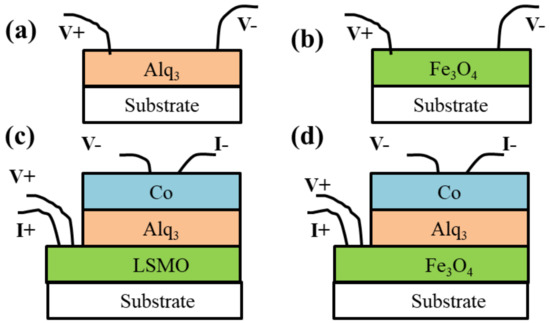
Figure 1.
Device structures of (a) Alq thin film with Cu/Al interconnects, (b) FeO thin films with Cu/Al interconnects, (c) FeO/Alq/Co magnetic tunnel junction(MTJ), (d) LaSrMnO (LSMO)/Alq/Co (MTJ).
3. Modeling and Assumptions
The paper presents a simple analytical model to investigate spin relaxation length in organic semiconductors and magnetic thin films. The computational process involves Matthiessen’s rule to combine the spin relaxation times due to various scatterings to obtain the net spin relaxation time given as,
where, , and are net, defect induced and phonon induced spin relaxation times, respectively. and can be replaced by their corresponding momentum relaxation times and following the relation,
where the index i corresponds to the i-th scattering mechanism, ‘a’ as spin-flip probability and is the corresponding spin-orbit coupling (SOC). This is a generalized model for the Elliot-Yafet spin scattering mechanism considering spin-orbit coupling induced hyperfine interaction [37,38].
The paper also presents a simple effective mass model with five parameters: (a) Equilibrium Fermi level E (b) Spin split fermi level, (c) Barrier height of the organic semiconductor, U (d) Effective masses for electrons inside FM contacts (m = m = m) and (e) effective mass for electrons inside organic spacer (m).
The three-dimensional band structure of organic semiconductors can be calculated using the semi-empirical intermediate neglect of differential overlap method. The method typically provides transfer integrals of the same magnitude as those obtained using DFT-based calculations. Under the model assumptions of constant relaxation time and fermi level carrier transport, the carrier mobility is found to be dependent on effective mass, whereas the effective mass is in turn dependent on band structure of the organic semiconductor [39].
Using these, we can understand different features of spin transfer torque (STT) devices like, (i) differential resistance, (ii) TMR, (iii) in-plane/out-of-plane STT etc. The model on spin transport is based on Non-Equilibrium Green’s Function (NEGF). Single band effective mass Hamiltonian H and self-energy are used to determine spin current densities, Green’s function, G(E), and electron correlation function G. Matched self-energy matrices have been used for both right and left magnetic leads as ballistic and coherent transport is considered across the MTJ devices. The retarded Green’s function (propagator) and electron correlation (density matrix) are calculated using Equations (3) and (4), respectively.
where G is the conjugate transpose of G(E). broadening matrices of the leads, and f are fermi functions of magnetic leads at energy E. Multiple transverse modes with wave vector k have been used for the analysis. H and are calculated, and hence spin current densities, G(E) and G have been extracted for each transverse mode. The results for each transverse mode are then used to find the current at any point using the following two equations:
The first current Equation (5) gives current between two terminals i and j, whereas the second one determines current between two points a and b. The indices (a,b) on the right-hand side of Equation (6) indicate specific matrix elements of the corresponding matrix. The resistance of MTJ is calculated using Equation (5) whereas the STT at free layer is calculated using Equation (6). The results so obtained are for single energy and single mode. The total current is then determined by taking double integral over all modes and energies between Fermi level windows of left and right magnetic electrodes. The details of mathematical modeling can be found in the supplementary section of the paper reported by Datta et al. [1].
4. Results and Discussion
We have investigated the effect of Alq width and thickness on spin relaxation length of conduction electrons across the organic semiconductor (Figure 2a). The modeling has been performed using spin transport modeling tool from nanohub database designed by Dincer et al. [2]. The compact model calculates spin-relaxation lengths and effective mean free path of carriers due to phonon-induced and defect-induced scatterings. The model parameters used for simulation have been taken from literature [3,4,5,6,7,8,9,10] and is depicted in Table 1. Spin relaxation length (L) is found to have a sharp rise at a small Alq width region, which eventually attains saturation at high width regime (Figure 2a). At a small width regime, the population of spin scattering sites may have been comparable with the distance between two consecutive scattering of a conduction electron within the organic semiconductor. The spin scattering sites considered are nonmagnetic and are mostly surface defects due to lattice distortion, which can precess due to coupling with local hyperfine field [15,37].
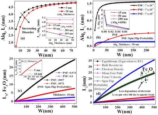
Figure 2.
(a) Spin Relaxation Length (L) variation with Film width (W), at 5 and 50 nm thicknesses, for Organic Semiconductor Alq considering coherent Spin injection and extraction. Inset shows the variation of L with Alq thickness at different Alq width (b) Variation of L with Alq width at different defect states induced spin-flip probabilities (PSF). Inset shows the variation of L with different PSF at different Alq width (c) Variation of L with FeO width at different FeO defect states induced spin-flip probability (PSF). Inset shows Spin Relaxation Length (L) variation with Film width (W), at 5 and 10 nm thicknesses, for FeO (d) Variation of L with FeO width for different deviated (from equilibrium values of Table 1) spin dependent transport parameters. A single profile indicates L change due to deviation of only that corresponding parameter. The other parameter values are fixed with values from Table 1.

Table 1.
Spin Transport dependent Model Parameters for Organic Semiconductor Alq and magnetic electrode FeO.
Though scattering sites increase with width, the predominant increase of the gap between scattering sites may have resulted in a sharp rise of L at a low width regime. However, further increase of scattering sites may have restricted further rise of L, eventually leading to saturation (width independent) at high width regime. This feature is well supported by electron mobility of Alq, which has been reported to follow its time-of-flight under applied external bias voltage [3]. Generally, spin relaxation in organic semiconductors is estimated using coupling of electron spins with hyperfine fields aided by hydrogen nuclei [10]. At high widths, a large scattering site population indicates high hyperfine coupling. Hence the coupling can be replaced by a classical, quasistatic, and random field distributed to a three-dimensional Gaussian (predominantly at high width regime) distribution [10]. Hence the spin diffusion at high width may be modeled as a combination of coherent and incoherent hopping in Gaussian density of states [10] around a local effective magnetic field. Moreover, spin-filtering across metal-Alq interfaces are affected by physisorbed interface states that are not spin split and hence follow a dynamic spin relaxation mechanism [40].
We consider that fully spins polarized carriers are injected into the organic semiconductor Alq, which moves towards the opposite electrode under the electric field (E). We assume that nearest neighbour hopping takes place by thermally assisted tunneling from site i to j with a rate for and for , where T is temperature, K is Boltzmann’s constant, and and are the on-site energies of sites i and j. The prefactor is related to a phonon attempt frequency and a factor related to wave function overlap. We consider a one-dimensional chain of sites for the case of for . By solving the Schrodinger equation for the spinor in effective magnetic field, exponential decay of polarization has been observed according to the expression ) where x is the distance from injection point of spin. The corresponding spin diffusion length L has been found to be , where is related to spin preservation through the semiconductor [10]. Considering the above transport conditions, exponential decay of L can be observed from Figure 2a at a low width regime.
We can also observe from the inset of Figure 2a a clear decrease of L with Alq thickness at a low width regime. An increase of thickness will incorporate more defect states leading to more hyperfine coupling and spin precession. Higher exponential decay at low width and higher thickness indicate fast loss of spin polarization due to deviation in site energy in-equation leading to . The increase in thickness will also reduce the hopping carrier transport as increase in will reduce the value of according the expression, [10]. Figure 2b shows variation of L with width for different spin-flip probability conditions. L has been observed to drastically decrease with an increase in spin-flip probability, indicating higher spin precession due to spin-flip scattering. Interestingly, we can also observe a reduction in the exponential nature of spin polarization decay with width reduction at higher spin-flip scattering (inset of Figure 2b). This may have occurred due to the reduction of hopping probability () of electrons on account of spin-flip scattering, which is also as per the analytical model discussed above.
We have tried to observe independently the modeling of spin transport through a FeO uniform film using the spin transport modeling tool [2]. The model parameters, at equilibrium, used for simulation are also depicted in Table 1. The values of the model parameters have been taken from literature [11,12,13]. Unlike Alq, a sharp change of spin relaxation length at a low width regime cannot be observed for FeO (Figure 2c). This indicates that the distance between scattering sites is comparable to the amount of spin-dependent scattering at those sites. A purely ferrimagnetic FeO may have an almost similar distance between consecutive pinning wells of adjacent defect states. Moreover, the defects are characterized by weak pinning strength owing to a small deviation from their intrinsic spin allignment [14]. As a result, similar energy will be required to depin the carriers from adjacent defect states [14]. Consequently, a characteristic linear rise of FeO spin relaxation length (L) can be observed with width from Figure 2c. Linearity in L versus w for FeO indicates a deviation from the hopping model, which well describes spin transport across FeO. Furthermore, a characteristic decrease in L can be observed with increased spin-flip probability in FeO (Figure 2c). Increased spin-flip probability (PSF) for FeO may be associated with the formation of pinning wells at defect states with strong pinning strength [14]. The conducting electrons change their spin orientation while coming out of the pinning well due to applied magnetic field. Hence increased PSF will increase the number of defect states with strong pinning strength which eventually reduce L in FeO. Interestingly, no change can be observed in L versus W profile for FeO with increasing film thickness (inset of Figure 2c). This indicates that most of the microstructural regions are not having defects or defects with small pinning strength [14] (simulation done maintaining minimum PSF). Hence within the provided thickness regime, spin-dependent scattering is very less, which gives minimum or zero deviation between both the curves, as shown in the inset of Figure 2c.
If we observe the reported experimental works on spin transport across Alq based organic spin valves, temperature-dependent MR quenching can be observed for the devices [22]. In order to understand the effect of the ferromagnetic electrode on MR quenching, we have observed the change in L due to the exclusive change of a single spin-dependent parameter (Figure 2d) without changing other parameters from Table 1. It is found that the mean free path in ferromagnets is associated with forming a dead layer within the active region of the electrode [23]. Hence, the mean free path for FeO will reduce at low temperatures due to a large number of defects with strong pinning strength [14]. This will eventually increase the attenuation of spin polarization, thereby reducing L(Figure 2d). Hence the reduction of the mean free path parameter of FeO (keeping other parameters constant with values shown in Table 1) will rather aid in reducing MR at low temperatures (Table 2). The bulk resistivity of FeO will increase with temperature reduction, thereby increasing spin frustration within the active layer. Hence the resistivity reduction will also lead to unusual MR reduction(Table 2 and Figure 2d) at low temperature [24] (keeping other parameters of FeO constant with values shown in Table 1). However, the electron density of FeO may decrease with increased resistivity at low temperatures. The decrease of FeO electron density and reduction of phonon-induced spin scattering have been independently observed to increase tunneling MR at low temperatures (Table 2). Hence it can be concluded that the MR values increased due to parameters like electron density, and phonon-induced spin flipping is rather compensated due to change in resistivity and mean free path of carriers in FeO at low temperature (Figure 2d). That is why experimentalists attribute the reason behind low-temperature high MR to reduced spin relaxation at the organic semiconductor layer of the device [22].
Table 2.
Model Parameters Deviation for FeO with temperature and its relation with change of TMR, provided other Parameters donot change their equilibrium values shown in Table 1.
After detailed analytical modeling on spin transport across FeO and Alq films, we have investigated tunnel magnetoresistance (TMR) across a FeO/Alq/Co hybrid MTJ (magnetic tunnel junction) device structure (Figure 3). Alq thickness is very thin compared to the magnetic electrodes. We have considered the device structure similar to the one we have fabricated previously for transport measurements [15]. The simulation has been performed using MTJ Lab tool from nanohub database designed by Ganguly et al. [16]. The model parameters used for simulation are depicted in Table 3 and are taken from previous literature reports [15,17].
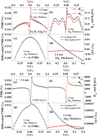
Figure 3.
(a) Voltage-dependent Tunnel Magnetoresistance (TMR) for FeO/Alq/Co MTJ (magnetic tunnel junction) device structure (b) Parallel and antiparallel resistances (R and R) versus voltage for MTJ structure (c) Differential TMR versus voltage for MTJ (d) Spin transfer torque (STT) versus voltage for the MTJ (e) Voltage-dependent Tunnel Magnetoresistance (TMR) for LaSrMnO/Alq/Co MTJ (magnetic tunnel junction) device structure (f) Parallel and antiparallel resistances (R and R) versus voltage for MTJ structure (g) Differential TMR versus voltage for MTJ (h) Spin transfer torque (STT) versus voltage for the MTJ.
Table 3.
FeO/Alq/Co and LSMO/Alq/Co MTJ parameters for tunnel magnetoresistance (TMR) simulations.
Figure 3a shows TMR versus voltage response for FeO/Alq/Co MTJ for different Alq thicknesses at room temperature. TMR refers to tunnel magnetoresistance across magnetic tunnel junctions, which indicate a change in resistance due to a change in the magnetization direction of the easy axis with applied magnetic field. The change of magnetization direction gives rise to parallel (R) and antiparallel (R) orientations of the magnetic electrodes resulting in TMR response mathematically represented by (R− R)/R. The values of TMR well match with the experimental data we got for similar FeO/Alq/Co structure [15]. An asymmetric nature of TMR response can be observed for the devices which is quite an established phenomenon [1,18,19]. Also the TMR decreases with the increase in the junction voltage (Figure 3). The Fermi energy, which decides the density of state of injection spin polarization, might be shifted under a relatively large applied bias voltage [20]; therefore, the effective spin polarization of FeO or Co might be modified [18]. The asymmetric voltage-dependent TMR response indicates different spin injection and spin extraction processes through Alq. We have already shown in our previous reports that FeO/Alq acts as a spin injecting interface at positive bias, whereas the same interface acts as a spin extraction region at negative bias [15]. Hence at positive bias, spin-polarized injection occurs owing to less spin-dependent scattering at FeO active layer of the device. That is why unlike negative bias, a sharp fall in TMR can be observed at a low positive bias regime (Figure 3a). We also observe a decrease in the sharp fall of TMR with an increase in Alq thickness (Figure 3a). The Alq film thicknesses, for MTJ, have been maintained within the limits of L (Figure 2b) we found from Figure 2b. The reduction of TMR, with thickness, at a low bias regime may be associated to spin relaxation at defect states within the optical band gap of the device [15]. The organic spacer is already found to have defect states from the published experimental reports [15]. The conduction electrons undergo spin canting due to coupling with local hyperfine fields within the device. We have further extracted resistance-voltage variation of the device both for parallel (R) and antiparallel (R) configurations as shown in Figure 3b. The difference between R and R is found to be higher at low bias voltages. This indicates spin precession at Alq defects do not affect spin-dependent scattering at magnetic layers for low voltage. However, less injection of spin-polarized electrons at high voltages makes the deviation between R and R smaller. Hence, TMR responses at different thicknesses have been observed to merge at high bias voltages (Figure 3a). Spin-polarized injection is also confirmed from differential TMR response, which shows the peak at low bias voltages (Figure 3c). Differential TMR gives information about the rate of change of TMR with applied voltage for the MTJ devices.
Figure 3d shows current induced in-plane and out-of-plane spin transfer torque (STT) versus bias voltage. It has been observed that the organic semiconductor can be used to generate in-plane STT on the magnetic layer, and the magnitude of STT increases with the increase of applied voltage. The change of in-plane STT with voltage may be associated with modified spin filtering at FeO/Alq and Alq/Co interfaces of the device [1,21]. Moreover, at low bias, spin conductances at magnetic electrodes are very small, which might have led to small in-plane STT across the device. The out-of-plane STT is negligibly small compared with the in-plane STT (Figure 3d) and is almost independent of applied voltage.
Figure 3e shows TMR versus voltage response for LSMO/Alq/Co hybrid MTJ at room temperature. The model parameters used for simulation are taken from literature [20,25,26] and is also shown in Table 3. We are trying to see the change of response if we replace FeO electrode by LSMO. Interestingly we received a very small TMR for the LSMO device compared to FeO device. A similar level of diminished MR response has also been observed from experimental results reported by Xiong et al. [27]. The Fermi level of LSMO at LSMO/Alq interface may have more scattering sites than FeO/Alq which diminishes the injection spin polarization of the LSMO device. Figure 4 shows the band structure of both LSMO and FeO based MTJ devices. The presence of interfacial dipoles at the FeO/Alq interface often gives rise to vacuum level offset, which generally shifts the non-interacting equilibrium energy levels of molecules towards a lower energy range (Figure 4a). However, this phenomenon is not that predominant with LSMO interfaces. The energy levels of the band structures have been taken from literatures [15,20]. We can also observe from the band structure that hole transport is predominant for both devices. The band offset between E (FeO) and HOMO (Alq) is much higher than E (LSMO) and HOMO (Alq). Hence carrier tunneling may predominate for FeO device, while band-band carrier injection may occur for LSMO-based devices. That may be why we have observed a higher TMR signal for the FeO device.
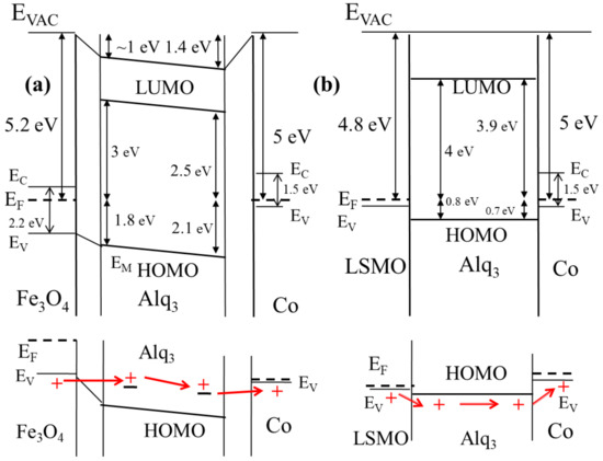
Figure 4.
(a) Upper section shows equilibrium band structure for FeO/Alq/Co MTJ. The lower section shows predominant tunneling across the optical band gap of the organic spacer region. (b) The upper section shows the equilibrium band structure for LSMO/Alq/Co MTJ. The lower section indicates predominant carrier injection across the organic semiconductor.
We have also extracted the resistance of LSMO device both for parallel and antiparallel orientation of the magnetic electrodes (Figure 3f). Almost negligible deviations between different orientations can be observed, resulting in a very small TMR response for the device. This means the overall change in resistance due to the spin scattering phenomenon is almost the same for both orientations. Predominant band-to-band carrier injection for LSMO device may have resulted in a loss of injection and detection spin polarization for the device. This resulted in a similar resistance-voltage profile for both orientations (Figure 3f). Therefore it is crucial for injection electrode Fermi level remain within the optical band gap of organic semiconductor to have tunneling phenomenon and hence good MR response. Unlike FeO device, no oscillations can be observed from R and R versus the voltage profile for the LSMO device. The oscillations in FeO device may be due to bias-induced modification of surface defects that induce field injection at the OSC optical gap of the device [15]. However, due to predominant carrier injection, such oscillations cannot be seen for LSMO devices. However, the peak from differential TMR response in Figure 3g indicates some injection of spin-polarized carriers at low bias voltages. The LSMO fermi level may have been within Alq optical gap for low bias, which eventually goes out of the gap at high bias resulting in a decrease of differential TMR within the device. Figure 3h shows in-plane and out-of-plane STT for LSMO device. The inplane STT shows a nonlinear change with voltage region, which is absent for FeO device. This also confirms the carrier injection phenomenon for LSMO devices which is somewhat lacking for FeO device. The out-of-plane STT response is almost similar to FeO device as the torque acts perpendicular to the magnetization direction of the magnetic electrodes.
Hence, this work of spin relaxation and defect states modulation in OSCs along with significant room temperature TMR will encourage realization of all-electrical highly non-volatile MRAM devices for low power magnetic recording applications.
5. Conclusions
In conclusion, we have analyzed modeling of phonon and defect-induced spin relaxation length (L) in FeO and organic semiconductor (OSC) Alq. A decrease in L of Alq with enhanced disorder and film thickness has been observed at a low film width regime. We have also found an exponential change of L at a low width regime for Alq. The change is, however, absent for FeO, indicating comparable spin-dependent scattering and L in FeO. L also decreases with spin-flip scattering both for Alq and FeO. Voltage-dependent tunnel magnetoresistance (TMR) response in LaSrMnO (LSMO)/Alq/Co and FeO/Alq/Co hybrid magnetic tunnel junction (MTJ) devices has been attributed to modified spin filter effect across magnetic/OSC junction at high bias regime. TMR reduction with Alq thickness for FeO device has been associated with spin relaxation at the organic spacer layer. We have also observed enhanced in-plane spin transfer torque for both MTJ, which may be associated with modified spin filtering at magnetic/OSC junctions. A smaller TMR signal for the LSMO device indicates reduced tunneling and enhanced carrier injection across the OSC, which is also supported by the band structure profile. The TMR response observed from simulation results is in accordance with previously reported experimental results. Higher TMR response for FeO device indicates the possibility of device employment in room temperature magnetic recording applications.
Author Contributions
D.D.: Writing—original draft, Visualization, Validation, Methodology, Resources, Investigation, Formal analysis; B.K.M.: Writing—review & editing, Visualization, Validation, Supervision, Project administration, Conceptualization. All authors have read and agreed to the published version of the manuscript.
Funding
This research received no external funding.
Data Availability Statement
The data that support the findings of this study are available within the article.
Conflicts of Interest
The authors declare that they have no known competing financial interests or personal relationships that could have appeared to influence the work reported in this paper.
References
- Datta, D.; Behin-Aein, B.; Datta, S.; Salahuddin, S. Voltage Asymmetry of Spin-Transfer Torques. IEEE Trans. Nanotechnol. 2011, 11, 261–272. [Google Scholar] [CrossRef]
- Dincer, O.; Naeemi, A. Spin Transport Modeling Tool. 2017. Available online: https://nanohub.org/resources/spintransport (accessed on 25 August 2022).
- Park, H.; Shin, D.-S.; Yu, H.-S.; Chae, H.-B. Electron mobility in tris (8-hydroxyquinoline) aluminum (Alq3) films by transient electroluminescence from single layer organic light emitting diodes. Appl. Phys. Lett. 2007, 90, 202103. [Google Scholar] [CrossRef]
- Halls, M.D.; Schlegel, H.B. Molecular Orbital Study of the First Excited State of the OLED Material Tris (8-hydroxyquinoline) aluminum (III). Chem. Mater. 2001, 13, 2632–2640. [Google Scholar] [CrossRef]
- Sito, J.; Grodzicki, M.; Lament, K.; Wasielewski, R.; Mazur, P.; Ciszewski, A. Electronic Properties of Structures Containing Films of Alq3 and LiBr Deposited on Si (111) Crystal. Acta Phys. Pol. A 2017, 132, 357–359. [Google Scholar] [CrossRef]
- Fong, H.H.; So, S.K. Hole transporting properties of tris (8-hydroxyquinoline) aluminum Alq3. J. Appl. Phys. 2006, 100, 094502. [Google Scholar] [CrossRef]
- Rashid, A.N.; Craig, D.C. Growth and Crystal Structure of Alq3 Single Crystals. A new structure showing π-π and CH-π interactions. Mrs Online Proc. Libr. 2004, 829, 393–401. [Google Scholar] [CrossRef]
- Groves, C. Simulating charge transport in organic semiconductors and devices: A review. Rep. Prog. Phys. 2016, 80, 026502. [Google Scholar] [CrossRef] [PubMed]
- Kanchibotla, B.; Pramanik, S.; Bandyopadhyay, S.; Cahay, M. Transverse spin relaxation time in organic molecules. Phys. Rev. B 2008, 78, 193306. [Google Scholar] [CrossRef]
- Bobbert, P.A.; Wagemans, W.; van Oost, F.W.A.; Koopmans, B.; Wohlgenannt, M. Theory for Spin Diffusion in Disordered Organic Semiconductors. Phys. Rev. Lett. 2009, 102, 156604. [Google Scholar] [CrossRef] [PubMed]
- Liu, H.; Valentin, C.D. Band Gap in Magnetite above Verwey Temperature Induced by Symmetry Breaking. J. Phys. Chem. C 2017, 121, 25736. [Google Scholar] [CrossRef]
- Bhatt, M.A.; Bhatt, P.J. Comparative analysis of dielectric strength and electron velocity in transformer oil based nanofluid. J. Eng. Sci. Technol. 2021, 16, 1167–1182. [Google Scholar]
- Brojabasi, S.; Muthukumaran, T.; Laskar, J.M.; Philip, J. The effect of suspended Fe3O4 nanoparticle size on magneto-optical properties of ferrofluids. Opt. Commun. 2014, 336, 278–285. [Google Scholar] [CrossRef]
- Deb, D.; Dey, P. Modeling of Temperature-Dependent Sign Reversal of Magnetoresistance in 99.95% La0.7Sr0.3MnO3–0.05% Paraffin Wax Nanocomposite: The Role of Pinning Center at Intergrain Defect Site. Phys. Stat. Solid. B 2019, 257, 1900402. [Google Scholar] [CrossRef]
- Deb, D.; Dey, P.; Choudhary, R.J.; Rawat, R.; Banerjee, A. Temperature dependent transition of conduction mechanism from carrier injection to multistep tunneling in Fe3O4 (111)/Alq3/Co organic spin valve. Org. Electron. 2021, 99, 106324. [Google Scholar] [CrossRef]
- Ganguly, S.; Datta, D.; Shang, C.; Ramadas, S.; Salahuddin, S.; Datta, S. Magnetic Tunnel Junction Lab. 2014. Available online: https://nanohub.org/resources/mtjlab (accessed on 25 August 2022).
- Barati, E.; Cinal, M.; Edwards, D.M.; Umerski, A. Gilbert damping in magnetic layered systems. Phys. Rev. B 2014, 90, 014420. [Google Scholar] [CrossRef]
- Liang, S.; Geng, R.; Yang, B.; Zhao, W.; Subedi, R.C.; Li, X.; Han, X.; Nguyen, T.D. Curvature-enhanced Spin-orbit Coupling and Spinterface Effect in Fullerene-based Spin Valves. Sci. Rep. 2016, 6, 19461. [Google Scholar] [CrossRef] [PubMed]
- Wang, F.; Vardeny, Z.V. Organic spin valves: The first organic spintronics devices. J. Mater. Chem. 2008, 19, 1685–1690. [Google Scholar] [CrossRef]
- Deb, D.; Nath, D.; Choudhary, R.J.; Roy, J.N.; Dey, P. Magneto-tunable photoresponse in ZnO-rGO/La0.7Sr0.3MnO3/ITO heterostructure: An opto-spintronic phenomenon. Phys. Lett. A 2022, 446, 128271. [Google Scholar] [CrossRef]
- Zhang, Q.; Chan, K.S.; Li, J. Spin-transfer torque generated in graphene based topological insulator heterostructures. Sci. Rep. 2018, 8, 434. [Google Scholar] [CrossRef] [PubMed]
- Devkota, J.; Geng, R.; Subedi, R.C.; Nguyen, T.D. Organic Spin Valves: A Review. Adv. Funct. Mater. 2016, 26, 3881–3898. [Google Scholar] [CrossRef]
- Tobin, J.G.; Morton, S.A.; Yu, S.W.; Waddill, G.D.; Schuller, I.K.; Chambers, S.A. Spin resolved photoelectron spectroscopy of Fe3O4: The case against half-metallicity. J. Phys. Condens. Matter. 2007, 19, 315218. [Google Scholar] [CrossRef] [PubMed]
- Dey, P.; Nath, T.K. Effect of grain size modulation on the magneto-and electronic-transport properties of La0.7Ca0.3MnO3 nanoparticles: The role of spin-polarized tunneling at the enhanced grain surface. Phys. Rev. B 2006, 73, 214425. [Google Scholar] [CrossRef]
- Bruno, F.Y.; Grisolia, M.N.; Visani, C.; Valencia, S.; Varela, M.; Abrudan, R.; Tornos, J.; Rivera-Calzada, A.; Unal, A.A.; Pennycook, S.J.; et al. Insight into spin transport in oxide heterostructures from interface-resolved magnetic mapping. Nat. Commun. 2015, 6, 6306. [Google Scholar] [CrossRef] [PubMed]
- Madon, B.; Kang, H.B.; Kang, M.G.; Maurya, D.; Magill, B.A.; Alves, M.J.P.; Wehrowe, J.-E.; Drouhin, H.-J.; Priya, S.; Khodaparast, G.A. Room temperature ferromagnetic resonance in hetero-epitaxial BTO-BFO/LSMO magnetoelectric composite. AIP Adv. 2018, 8, 105034. [Google Scholar] [CrossRef]
- Xiong, Z.H.; Wu, D.; Vardeny, Z.V.; Shi, J. Giant magnetoresistance in organic spin-valves. Nature 2004, 427, 821–824. [Google Scholar] [CrossRef] [PubMed]
- Yang, X.; Guo, A.; Guo, L.; Liu, Y.; Sun, X.; Guo, Y. Organic Semiconductors for Room-Temperature Spin Valves. ACS Mater. Lett. 2022, 4, 805–814. [Google Scholar] [CrossRef]
- Majumdar, S.; Majumdar, H.S. Decay in spin diffusion length with temperature in organic semiconductors—An insight of possible mechanisms. Synth. Met. 2013, 173, 26–30. [Google Scholar] [CrossRef]
- Jang, H.-J.; Richter, C.A. Organic Spin-Valves and Beyond: Spin Injection and Transport in Organic Semiconductors and the Effect of Interfacial Engineering. Adv. Mater. 2016, 29, 1602739. [Google Scholar] [CrossRef] [PubMed]
- Poggini, L.; Cucinotta, G.; Pradipto, A.-M.; Scarrozza, M.; Barone, P.; Caneschi, A.; Graziosi, P.; Calbucci, M.; Cecchini, R.; Dediu, V.A.; et al. An Organic Spin Valve Embedding a Self-Assembled Monolayer of Organic Radicals. Adv. Mater. Interfaces 2016, 3, 1500855. [Google Scholar] [CrossRef]
- Van Schijndel, M.J.M. Novel Experimental and Modeling Approaches to Organic Spin-Valves. Master’s Thesis, University of Technology, Eindhoven, The Netherlands, 2010. [Google Scholar]
- Shi, S. Theory and Modeling for Organic Spintronics and Electronics. Ph.D. Thesis, University of Minnesota, Minneapolis, MN, USA, 2017. [Google Scholar]
- Goswami, A.; Yunus, M.; Ruden, P.P.; Smith, D.L. Magneto-resistance of organic spin valves due to spin-polarized tunnel injection and extraction of charge carriers. J. Appl. Phys. 2012, 111, 034505. [Google Scholar] [CrossRef]
- Lian, H.; Cheng, X.; Hao, H.; Han, J.; Lau, M.-T.; Li, Z.; Zhou, Z.; Dong, O.; Wong, W.-Y. Metal-containing organic compounds for memory and data storage applications. Chem. Soc. Rev. 2022, 51, 1926–1982. [Google Scholar] [CrossRef] [PubMed]
- Lin, H.; Luo, X.; Liu, L.; Wang, D.; Zhao, X.; Wang, Z.; Xue, X.; Zhang, F.; Xing, G. All-Electrical Control of Compact SOT-MRAM: Toward Highly Efficient and Reliable Non-Volatile In-Memory Computing. Micromachines 2022, 13, 319. [Google Scholar] [CrossRef] [PubMed]
- Rakheja, S.; Chang, S.-C.; Naeemi, A. Impact of Dimensional Scaling and Size Effects on Spin Transport in Copper and Aluminum Interconnects. IEEE Trans. Electron. Devices 2013, 60, 3913–3919. [Google Scholar] [CrossRef]
- Sharkas, K.; Pritchard, B.; Autschbach, J. Effects from Spin–Orbit Coupling on Electron-Nucleus Hyperfine Coupling Calculated at the Restricted Active Space Level for Kramers Doublet. J. Chem. Theory Comput. 2014, 11, 538–549. [Google Scholar] [CrossRef] [PubMed]
- Yang, Y.; Geng, H.; Yin, S.; Shuai, Z.; Peng, J. First-principle Band Structure Calculations of Tris(8-hydroxyquinolinato) aluminum. J. Phys. Chem. B 2006, 110, 3180–3184. [Google Scholar] [CrossRef] [PubMed]
- Droghetti, A.; Thielen, P.; Rungger, I.; Haag, N.; Gromann, N.; Stockl, J.; Stadtmuller, B.; Aeschlimann, M.; Sanvito, S.; Cinchetti, M. Dynamic spin filtering at the Co/Alq3 interface mediated by weakly coupled second layer molecules. Nat. Commun. 2016, 7, 12668. [Google Scholar] [CrossRef]


Publisher’s Note: MDPI stays neutral with regard to jurisdictional claims in published maps and institutional affiliations. |
© 2022 by the authors. Licensee MDPI, Basel, Switzerland. This article is an open access article distributed under the terms and conditions of the Creative Commons Attribution (CC BY) license (https://creativecommons.org/licenses/by/4.0/).