Article

Crystalline Phase Segregation of Quantum-Dots-Passivated CH3NH3PbI3 Film via Argon Plasma Treatment

1
School of Ocean Information Engineering, Jimei University, Jimei District, Xiamen 361021, China
2
Department of Applied Physics, National University of Kaohsiung, Kaohsiung University Rd., Kaohsiung 81148, Taiwan
3
Department of Mechatronic Engineering, National Taiwan Normal University, Heping East Rd., Taipei 10610, Taiwan
4
Department of Electronic Engineering, Center for Environmental Toxin and Emerging−Contaminant Research, Super Micro Mass Research & Technology Center, Cheng Shiu University, Chengcing Rd., Kaohsiung 82146, Taiwan
*
Authors to whom correspondence should be addressed.
Crystals 2022, 12(11), 1556; https://doi.org/10.3390/cryst12111556
Submission received: 15 September 2022 / Revised: 13 October 2022 / Accepted: 25 October 2022 / Published: 31 October 2022
(This article belongs to the Special Issue Solution-Based Processes in Semiconductors and Electronic Devices)

Abstract

:
In this study, a composite perovskite film composed of lead cesium triiodide (CsPbI3) quantum dots (QDs) and methylammonium lead iodide (CH3NH3PbI3; MAPbI3) was proposed. The CsPbI3 QDs prepared by hot-injecting were used as an anti-solvent in precursors to passivate the surface of this composite perovskite film. The further argon (Ar) plasma treatment improves the surface of the film. The effects of the powers from 100 to 200 W on the composite perovskite film structure, chemical element composition, and optical properties were studied. The experimental results demonstrate that the CsPbI3 QDs passivation boosts the ultraviolet light absorption (350–450 nm) and inhibits the formation of the PbI2 phase. Furthermore, Ar plasma treatment effectively improved CsPbI3 QDs passivation on MAPbI3 film. The powers lower than 140 W cause C=O bonds to dissolve and coordination bonds to form between OA carboxyl moieties and undercoordinated Pb2+ ions. At 160 and 140 W, the obvious crystal phase segregation and a decrease in light absorption are observed, respectively. Meanwhile, the strong bombardment of Ar ions at higher than 160 W causes the severe degradation of MAPbI3 film.

1. Introduction

Over the past several decades, a variety of optoelectronic devices, such as solar cells [1,2,3], light-emitting diodes [4,5], and photo-detectors [6,7], have made extensive use of the metal halide perovskite thin film as a potential material due to its promising optical and electrical properties. Especially, this great potential appearing in revolutionary renewable energy applications is mainly attributed to a series of high absorption coefficients, tunable optical band gaps, high charge mobility, long carrier lifetime, and small exciton binding energy [8,9,10,11]. In general, however, it is well-known that defect formation is unavoidable on the surfaces, interfaces, and grain boundaries of perovskite polycrystalline films, which can lead to the recombination of photo-generated carriers and inhibit the splitting of quasi-Fermi. Besides, the degradation of perovskite causing the decrease in device stability is still mainly attributed to the generation of ion migration channels [12] induced by the surface and interfacial defects, despite metal halide perovskite usually acting as a defects-tolerant semiconductor material [13]. Therefore, these results suggest that the development of defect engineering can play an important factor in further improving the film quality and optoelectrical properties. Comprehensibly driven by lots of efforts, including composition adjusting [14], passivation on surface and interface [15,16,17], heterojunction engineering [18], and the introduction of additive [19,20], one of the optimization engineerings for the perovskite film quality can be focused on the hetero−atomic doping techniques to increase the film compactness and decrease the defect formation. The hetero−atomic doping techniques are a common way of introducing atoms of different elements into the lattice [21,22,23], suggesting the inorganic perovskite quantum dots (QDs) material is a proper candidate owing to the difference in the element of the cation site. For example, Feng Hao et al. improved the crystallinity and reduced the trap density of the methylammonium lead iodide (CH3NH3PbI3, MAPbI3) by doping Cl−HOBT [24]. Niu, G et al. enhanced the photoelectric conversion efficiency of MAPbI3 solar cells by introducing Cs ions [25,26], proving the interaction of organic and inorganic functional groups can reduce the degradation of perovskite films [27].
Currently, the cesium triiodide (CsPbI3) is a suitable QDs capping with the hydrophobic ligands. It is found that the organic ligands attached to CsPbI3 QDs can self−assemble on interfaces and grain boundaries for defect passivation [28,29]. Meanwhile, the hydrophobic QDs can be well combined into metal halide perovskite thin films through ion exchange and diffusion [30,31,32,33], benefiting from their soft ion lattice. However, the crystalline structure of thin films is usually constructed by annealing, leading to the nanocrystal’s mutual merging into large crystalline grains due to Ostwald ripening [34,35,36] although there is some partial cluster distribution of organic contaminants or by-products. The subsequent surface treatment of Argon (Ar) plasma is the preferred method for removing organic contaminants from incomplete ion exchange or reaction, even further optimizing the morphologies of thin films. In many studies related to metal oxides or organic materials [27,37,38,39,40], the plasma excited by a single or lots of species of gas is often used for surface pretreatment or post-treatment. Nevertheless, excess power or exceeding operating time will lead to the degradation where MAPbI3 converts to PbI2, inferring the ion bombardment with high energy will even cause damage to the surface and crystalline structure. These disadvantages demonstrate that the proper parameter window of Ar plasma is necessary to improve the surface morphologies and thus initiate the generation of dangling bonds on the surface in the future.
In this paper, a useful approach by adding CsPbI3 QDs into MAPbI3 thin film during the anti-solvent spin-coating process was proposed. Subsequently, this composite perovskite film was further treated by Ar plasma with varying powers from 100 to 200 W. The effects of power on the crystalline structure, chemical binding characteristics, and the absorption of the composite perovskite film are investigated to illustrate a solution to suppressing phase segregation.

2. Materials and Methods

2.1. Materials

Table 1 shows all materials without further purification. Before plasma treatment, the preparation was in a glove box with moisture and oxygen gas of a lower value than 1 ppm.

2.2. Synthesis Process of MAPbI3 and Cs-Oleate Precursor

The MAPbI3 precursor solution was mixed by adding methylammonium iodide (CH3NH3I), lead(II) iodide (PbI2), and dimethyl sulfoxide (DMSO, C2H6OS) and then stirred for 24 h at 300 rpm. The Cs-oleate precursor was mixed by adding Cs2CO3, oleic acid (C18H34O2), and 1-octadecene (C18H36) and stirred for 1 h at 120 °C to remove the moisture and internal air of the solution. Finally, this Cs-oleate precursor was stored below/at 100 °C.

2.3. Synthesis and Purification Process of CsPbI3 QDs

First, to prepare the clear CsPbI3-QDs solution with the completely dissolved PbI2, the C18H36 and PbI2 were mixed under continuous stirring for 1 h at 120 °C before adding the C18H34O2 and (Z)-Octadec-9-enylamine (C18H35NH2) solution preheated at 70 °C. Second, the Cs-oleate precursor was rapidly injected into the CsPbI3-QDs solution preheated at 185 °C and cooled after 5 s to terminate the reaction. Third, the methyl acetate (MeOAc, CH3COOCH3) was added into CsPbI3-QDs solution at a volume ratio of 1:3 (v/v) and then centrifuged at 8000 rpm for 5 min to accomplish the purification. The layered solution is clearly observed between the supernatant solution and precipitate, where the supernatant solution was sucked to obtain the precipitate. This precipitate was dissolved into a 1:1 (v/v) MeOAc/hexane (C6H14). Then, it was centrifuged at 8000 rpm for 5 min again to obtain the CsPbI3-QDs precipitate. Finally, repeating the previous steps, the CsPbI3-QDs precipitate was dispersed again and then residual substances including C18H34O2, C18H36, and PbI2 were removed by centrifuging at 4000 rpm for 5 min. The high-purity CsPbI3 QDs particles were obtained by sucking the supernatant solution.

2.4. Growth of the Composite Perovskite Film

50 μL MAPbI3 and 1 mg CsPbI3 QDs mixed were statically spin-coated on a substrate in two steps, where the first step is at 1000 rpm for 10 s and the second step is at 5000 rpm for 20 s. Toluene was dropped on the spined film for 15 s during the second step. The composite perovskite film was annealed at 80 °C for 15 min and then further treated by Ar plasma. The thickness of the film is about 210 nm.

2.5. Characteristic Measurements

The absorbance of all samples was determined by an ultraviolet/visible (UV/vis) spectrophotometer (U-3900, HITACHI, Tokyo, Japan) in the range of 350−850 nm. The structural characteristics and chemical states of the core-level of composition elements were detected by the grazing incidence X-ray diffraction measurement (GIXRD, Bruker D8 Discover, Billerica, MA, USA) and X-ray photoelectron spectroscopy (XPS, ULVAC-PHI, Chigasaki, Japan), respectively.

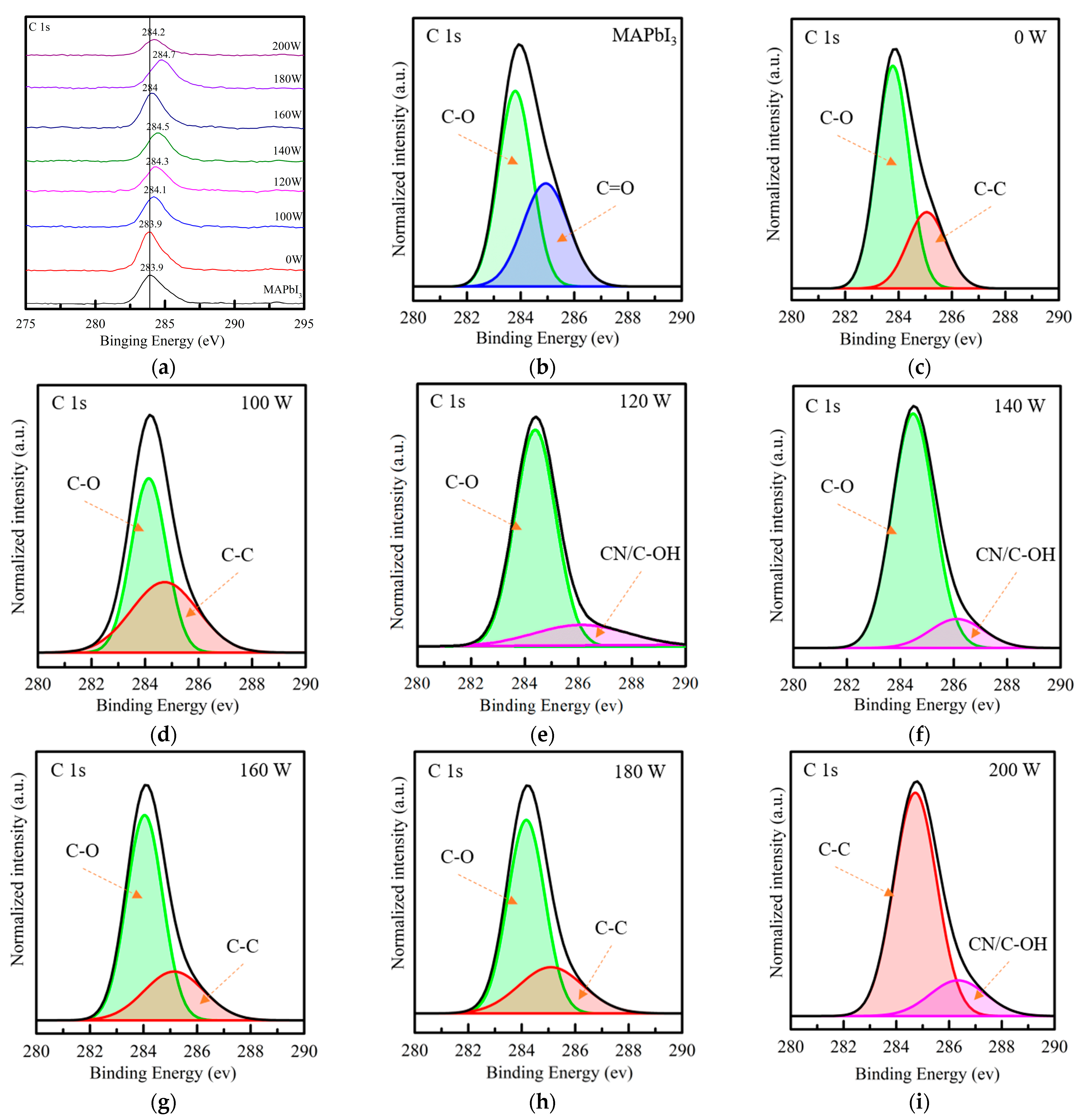
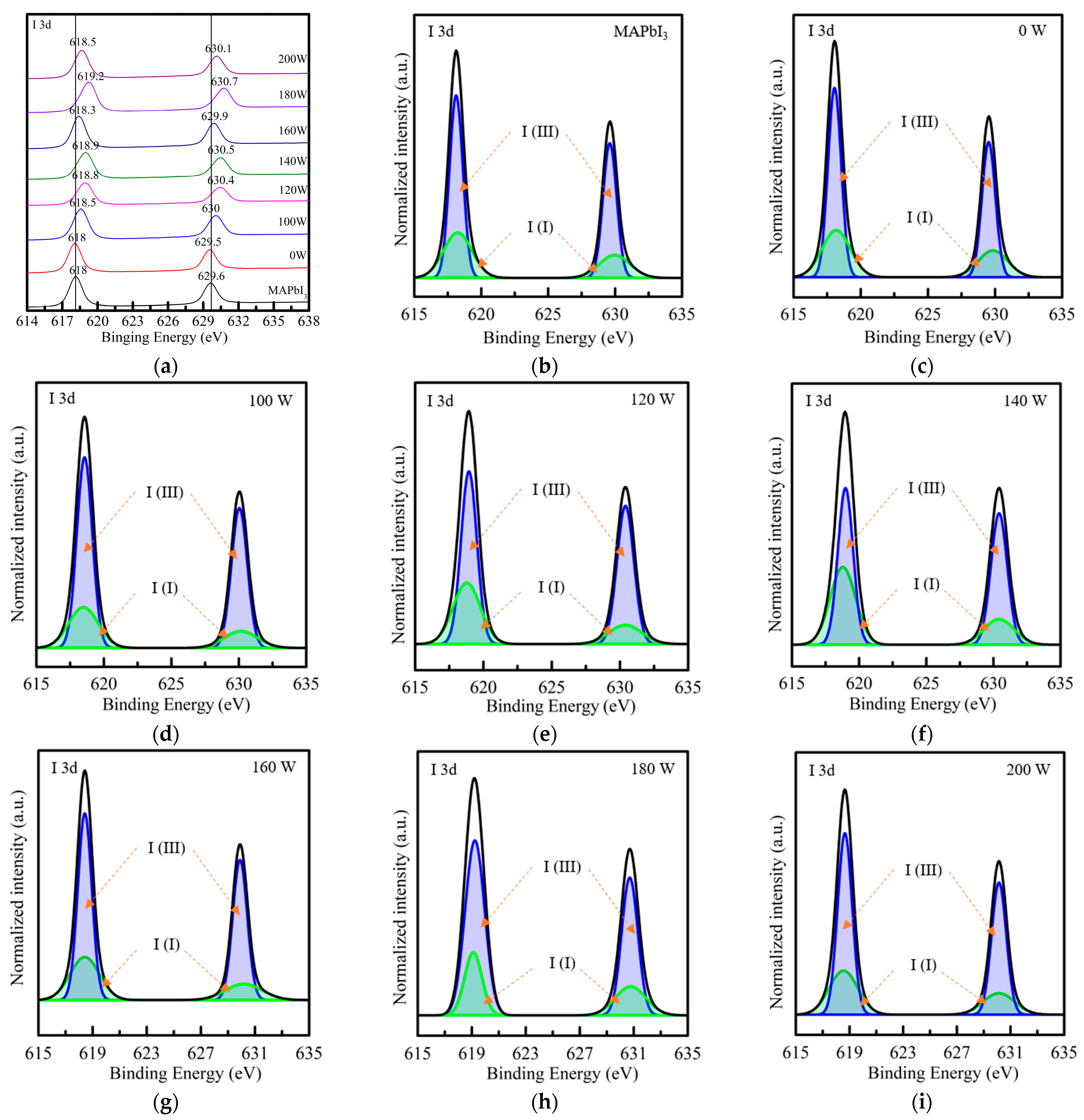
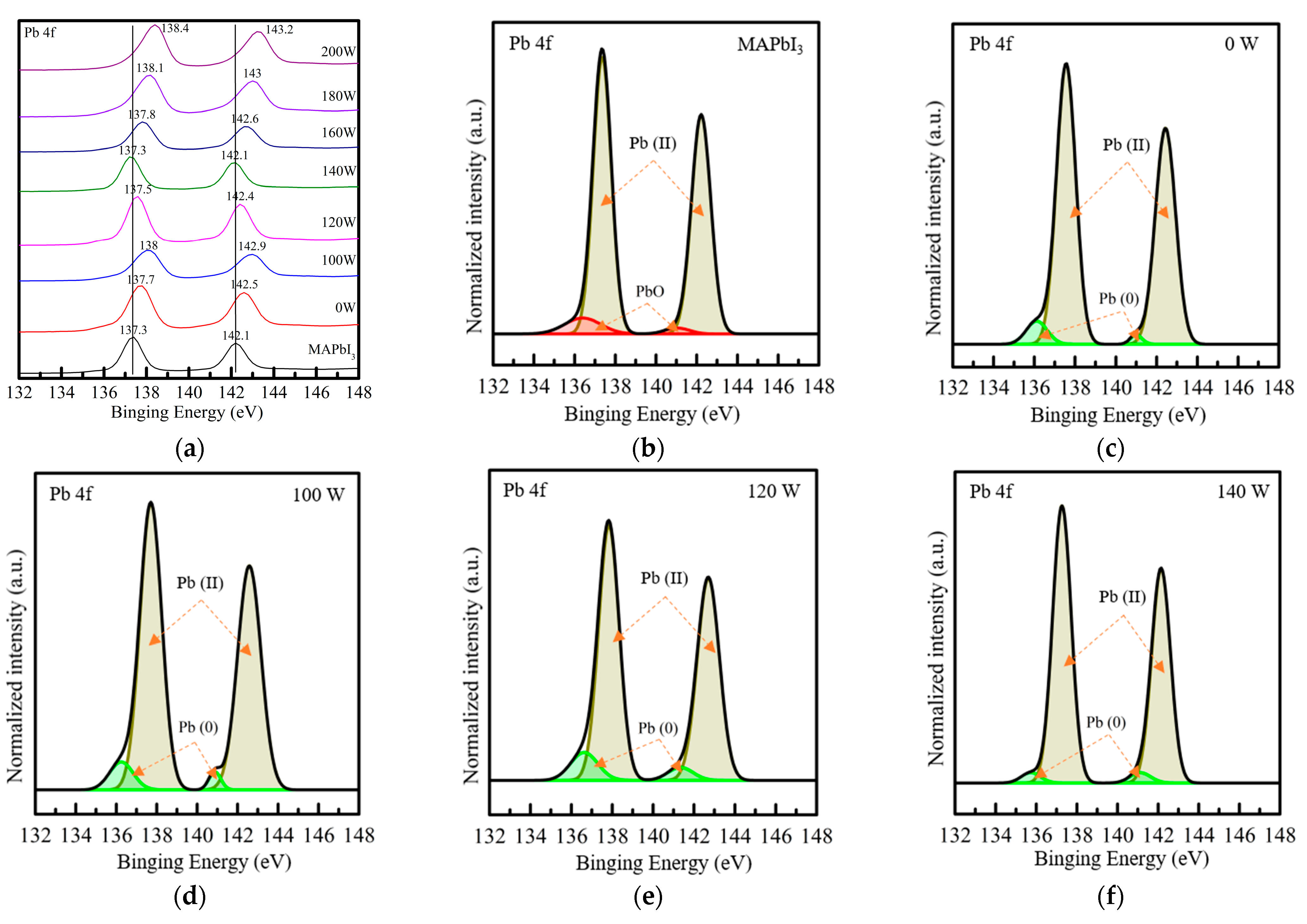
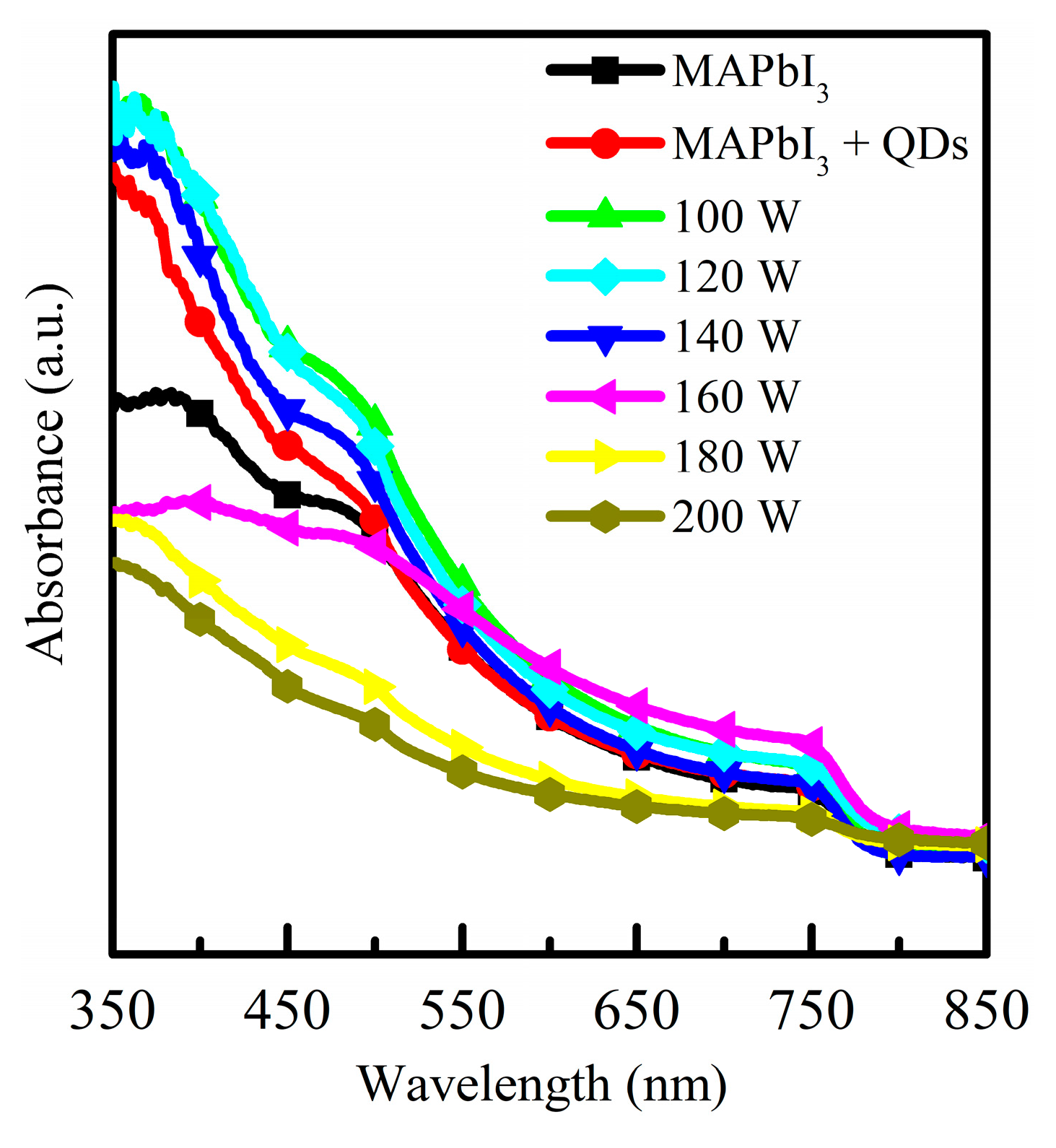
3. Results and Discussion

To confirm the crystalline structure, the X-ray diffraction (XRD) patterns of the composite perovskite films with different Ar plasma powers are shown in Figure 1. The peaks at 12.65°, 14.09°, 28.47°, 38.69°, and 52.40° correspond to the strongest (001), (110), (220), (003) and (004) phases. Compared to the MAPbI3 films, the CsPbI3 QDs-doped samples did not have any observed peaks, which is in agreement with other studies majoring in the doping of organic or inorganic materials [41]. This result demonstrates the effective inhibition of the PbI2 phase due to the decrease of hydrogen bonds in MAPbI3 and the increase of the octahedral tilt during the exchange process of Cs ions [42,43]. As the samples are treated by Ar plasma, an additional peak is observed at 12.7° and assigned to the PbI2 of the (001) phase. The excess ligands such as oleylamine and oleic acid are removed when the power is lower than 140 W. With powers higher than 160 W, the degradation of MAPbI3 and PbI2 is observed due to the bombardment of the excess ion energy. Figure 1b shows the details of the preferred (110) peaks of the CsPbI3 QDs doped MAPbI3. The asymmetric (100) peak at 13.97° can be deconvoluted to the presence of CsPbI3 QDs. The shift of peak toward a lower angle from 14.15° at 100 W from 14.11° at 140 W suggests the lattice contraction by the calculation of the interplanar distance of the Bragg formula. This result can also be proved by the XPS measurement, revealing the decrease in vacancies defects of iodine anion. However, the powers higher than 140 W remove the surface contaminants due to the bombardment of Ar ion, similar to a previous study [40].
The elemental state and distribution of MAPbI3 film with and without CsPbI3 QDs passivation were measured by XPS to explore the core-level spectra of C 1s, I 3d, and Pb 4f. The asymmetric peaks of C 1s are observed in Figure 2. Figure 2a,b shows the deconvoluted spectrum of the binding energy of C 1s in the MAPbI3 film with and without CsPbI3 QDs-passivation, suggesting the binding state of carbon material and atmospheric oxygen where the C-O and C=O peaks are respectively located at 283.97 and 285.4 eV [44]. The reason is attributed to the combination of carbon configuration and oxygen on the surface of MAPbI3 film, which is due to the oxidation by the moisture in the atmosphere. However, the C-O peak shifts towards higher binding energy and converts to the C-C peak owing to the CsPbI3 QDs passivation. As shown in Figure 2c–h, with the increasing Ar plasma powers from 100 to 200 W, the powers of 120, 140, and 200 W demonstrate the CN/C-OH peak assigned to 286.1 eV. The C-C peak is observed as the power higher than 160 W, eliminating the organic components with the weaker bonding. The proportion of carbon-related substances can be calculated by the area under each curve, demonstrating that excessive powers higher than 160 W cause the increasing C-C related substances and the removal of the C-O related substances, although the reappearance of the CN/C-OH related substances at 200 W is possibly due to the physical resultants bombarded by Ar ions.
To investigate the effects of QDs-passivation and plasma powers on the halide anion, Figure 3a shows the XPS core-level spectra of I 3d3/2 and 3d5/2 peaks assigned at 619 eV and 631 eV, respectively. The two binding energies of I 3d peaks for the MAPbI3 film and CsPbI3 QDs-passivated MAPbI3 film are demonstrated in Figure 3b,c. The spectra of I 3d can be deconvoluted to I3− ion (assigned at 619.5 and 631 eV) and I2+ ion (assigned at 619.37 and 630.87 eV), respectively. No obvious shift of binding energy for the samples with and without QDs-passivation is observed. This result needs further evidence for the variation of the core-level spectra of Pb 4f. Meanwhile, it is observed that with the increasing Ar plasma powers, as shown in Figure 3d–i, the position of these two peaks slightly shift to higher binding energy in the range of 140 to 180 W and then shifts back to the original one at 200 W. The shift towards higher binding energy is generally associated with anion vacancies [45]. Excessive plasma power induces heating, leading to the generation of iodine vacancies by heat-driven deiodination, which is similar to the research [46].
On the other hand, Figure 4a illustrates the XPS core-level spectra of Pb 4f. As shown in Figure 4b, the deconvoluted result of the metallic Pb4+ ion corresponds to 136.23 and 141.18 eV whereas the binding energies of 138.07 and 142.97 eV represent the result of the Pb2+ ion in composite perovskite films in Figure 4c. Compared to the result of the MAPbI3 film, the apparent ~0.4 eV shift of peak position toward the higher binding energy reveals that the QDs-passivated samples demonstrate a donor-acceptor complex formed by the Iodine atom and Lead atom. This result is attributed to the excess unpaired electrons provided by the low electronegativity Pb atom to the high electronegativity Iodine (I). The oxidation of the Pb atom to Pb2+ refers to the reduction of (I + 2 e→to 2 I) and further reduces the triiodide substances in the process of electron transfer. When the power increases, as shown in Figure 4d–i, a maximum shift toward lower binding energy observed at 140 W suggests the formation of coordination bonds between carboxyl moieties from OA and undercoordinated Pb2+ ions [17]. This result reveals that the MA site is replaced by the more stable Cs atom, effectively suppressing the unsaturated Pb owing to the less loss of molecular groups and iodide atoms at the A site of perovskite. A power higher than 140 W reveals a peak shift toward the higher binding energy, possibly due to the reorganization site from metallic Pb, referring to the unsaturated Pb which is associated with the lack of iodide substances [47].
Figure 5 illustrates the absorption spectrums of the composite perovskite films treated by Ar plasma at different powers from 100 to 200 W. The doping of CsPbI3 QDs increases the absorption of the MAPbI3 film in the range of 350–500 nm. The reason is the CsPbI3 QDs with wide energy gap value causes a shift of the absorption edge towards short wavelengths [41,48]. Multiple studies demonstrated that the absorption capacity of the perovskite film could be enhanced by doping with QDs [3,49]. With the increasing Ar plasma power, it can be seen that the samples at a power lower than 140 W present the highest absorption of films due to the removal of excess ligands and impurities on the surface. As the power is 160 W, the decrease in absorption observed is due to the degradation of MAPbI3. The higher 180 and 200 W cause the decrease of absorption observed at wavelengths range of 350–500 and 750 nm owing to the severe surface damage from ion bombardment. This ion bombardment leads to the structural change of the film surface corresponding to the decomposition of MAPbI3. The decomposition of MAPbI3 can be seen by the visible color change from dark brown to yellow, which is similar to other studies and our previous reports [50,51]. On the other hand, the surface morphologies of films are observed as shown in Figure S1. The film surface without plasma treatment shows irregular clusters, possibly containing some organic ligands. At 100 W, the film shows a schistose-like surface with unclear boundaries. A clear schistose-like surface at 120 W observed has clearer grain and boundaries. With the increasing power, the ion bombardment from Ar plasma causes severe damage to the surface.

4. Conclusions

The CsPbI3 QDs passivated-MAPbI3 film prepared by anti-solvent engineering was proposed. This composited perovskite film was further treated by different Ar plasma powers from 100 to 200 W. The XRD and XPS are used to research the effects of the passivation and the increasing powers on the composited perovskite films. At 160 W, the obvious segregation of the crystal phase is owing to the formation of the PbI2 phase of (001), (003), and (004), implying high ion energy degraded MAPbI3 and PbI2. The powers lower than 140 W removes extra ligands of oleylamine and oleic acid. The shift of Pb 4f peaks towards lower binding energy indicates the formation of coordination bonds between carboxyl moieties and undercoordinated Pb2+ ions due to excess unpaired electrons given by the low electronegativity Pb atom to the high electronegativity Iodine (I). The C-O peak shifts towards higher binding energy and converts to the C-C peak due to CsPbI3 QDs passivation, resulting in enhanced composite perovskite film absorbance due to the shift of the absorption edge towards short wavelengths. Therefore, the Ar plasma as a potential treatment not only effectively eliminates the organic contaminants from the film surface and inhibits or promotes crystal segregation, referring to surface defect passivation.

Supplementary Materials

The following are available online at https://www.mdpi.com/article/10.3390/cryst12111556/s1, Figure S1: The surface morphologies of composited films treated by Ar plasma at differnet powers from (a) 0 W to (g) 200 W.

Author Contributions

Conceptualization, P.-H.H., S.-Y.L., C.-H.L. and N.-F.W.; methodology, P.-H.H. and S.-Y.L.; Formal analysis, P.-H.H., S.-Y.L., C.-H.L. and C.-J.H.; Investigation, P.-H.H., S.-Y.L. and C.-J.H.; resources, S.-Y.L. and C.-J.H.; data curation, S.-Y.L. and P.-H.H.; writing—original draft preparation, P.-H.H. and S.-Y.L.; writing—review and editing, C.-H.L., N.-F.W. and C.-J.H.; project administration, P.-H.H., S.-Y.L. and C.-J.H.; funding acquisition, S.-Y.L. and C.-J.H.; supervision, C.-H.L., N.-F.W. and C.-J.H. All authors have read and agreed to the published version of the manuscript.

Funding

This work is sponsored by the National Science and Technology Council (NSTC) of the Republic of China under contact numbers of 110-2221-E-390-019 and 111-2221-E-390-017.

Institutional Review Board Statement

Not applicable.

Informed Consent Statement

Not applicable.

Data Availability Statement

Not applicable.

Conflicts of Interest

The authors declare no conflict of interest.

References

  1. Guo, F.; Qiu, S.; Hu, J.; Wang, H.; Cai, B.; Li, J.; Yuan, X.; Liu, X.; Forberich, K.; Brabec, C.J.; et al. A Generalized Crystallization Protocol for Scalable Deposition of High—Quality Perovskite Thin Films for Photovoltaic Applications. Adv. Sci. 2019, 6, 1901067. [Google Scholar] [CrossRef] [PubMed] [Green Version]
  2. Li, Y.; Shi, J.; Zheng, J.; Bing, J.; Yuan, J.; Cho, Y.; Tang, S.; Zhang, M.; Yao, Y.; Lau, C.F.J.; et al. Acetic Acid Assisted Crystallization Strategy for High Efficiency and Long—Term Stable Perovskite Solar Cell. Adv. Sci. 2020, 7, 1903368. [Google Scholar] [CrossRef] [PubMed] [Green Version]
  3. Chen, L.-C.; Tien, C.-H.; Tseng, Z.-L.; Ruan, J.-H. Enhanced Efficiency of MAPbI3 Perovskite Solar Cells with FAPbX3 Perovskite Quantum Dots. Nanomaterials 2019, 9, 121. [Google Scholar] [CrossRef] [PubMed] [Green Version]
  4. Liang, H.; Yuan, F.; Johnston, A.; Gao, C.; Choubisa, H.; Gao, Y.; Wang, Y.; Sagar, L.K.; Sun, B.; Li, P.; et al. High Color Purity Lead—Free Perovskite Light—Emitting Diodes via Sn Stabilization. Adv. Sci. 2020, 7, 1903213. [Google Scholar] [CrossRef] [PubMed] [Green Version]
  5. Liu, Z.; Lin, C.-H.; Hyun, B.-R.; Sher, C.-W.; Lv, Z.; Luo, B.; Jiang, F.; Wu, T.; Ho, C.-H.; Kuo, H.-C.; et al. Micro-Light-Emitting Diodes with Quantum Dots in Display Technology. Light Sci. Appl. 2020, 9, 83. [Google Scholar] [CrossRef] [PubMed]
  6. Wang, H.; Li, S.; Liu, X.; Shi, Z.; Fang, X.; He, J. Low-Dimensional Metal Halide Perovskite Photodetectors. Adv. Mater. 2021, 33, 2003309. [Google Scholar] [CrossRef]
  7. Zeng, L.; Chen, Q.; Zhang, Z.; Wu, D.; Yuan, H.; Li, Y.; Qarony, W.; Lau, S.P.; Luo, L.; Tsang, Y.H. Multilayered PdSe2/Perovskite Schottky Junction for Fast, Self—Powered, Polarization-Sensitive, Broadband Photodetectors, and Image Sensor Application. Adv. Sci. 2019, 6, 1901134. [Google Scholar] [CrossRef] [Green Version]
  8. Shi, L.; Bucknall, M.P.; Young, T.L.; Zhang, M.; Hu, L.; Bing, J.; Lee, D.S.; Kim, J.; Wu, T.; Takamure, N.; et al. Gas Chromatography–Mass Spectrometry Analyses of Encapsulated Stable Perovskite Solar Cells. Science 2020, 368, eaba2412. [Google Scholar] [CrossRef]
  9. Xu, J.; Boyd, C.C.; Yu, Z.J.; Palmstrom, A.F.; Witter, D.J.; Larson, B.W.; France, R.M.; Werner, J.; Harvey, S.P.; Wolf, E.J.; et al. Triple-Halide Wide–Band Gap Perovskites with Suppressed Phase Segregation for Efficient Tandems. Science 2020, 367, 1097–1104. [Google Scholar] [CrossRef]
  10. Hu, L.; Peng, J.; Wang, W.; Xia, Z.; Yuan, J.; Lu, J.; Huang, X.; Ma, W.; Song, H.; Chen, W.; et al. Sequential Deposition of CH 3 NH 3 PbI 3 on Planar NiO Film for Efficient Planar Perovskite Solar Cells. ACS Photonics 2014, 1, 547–553. [Google Scholar] [CrossRef]
  11. Wang, Z.; Wang, P.; Wang, F.; Ye, J.; He, T.; Wu, F.; Peng, M.; Wu, P.; Chen, Y.; Zhong, F.; et al. A Noble Metal Dichalcogenide for High-Performance Field—Effect Transistors and Broadband Photodetectors. Adv. Funct. Mater. 2020, 30, 1907945. [Google Scholar] [CrossRef]
  12. Kim, M.; Motti, S.G.; Sorrentino, R.; Petrozza, A. Enhanced Solar Cell Stability by Hygroscopic Polymer Passivation of Metal Halide Perovskite Thin Film. Energy Environ. Sci. 2018, 11, 2609–2619. [Google Scholar] [CrossRef]
  13. Ni, Z.; Bao, C.; Liu, Y.; Jiang, Q.; Wu, W.-Q.; Chen, S.; Dai, X.; Chen, B.; Hartweg, B.; Yu, Z.; et al. Resolving Spatial and Energetic Distributions of Trap States in Metal Halide Perovskite Solar Cells. Science 2020, 367, 1352–1358. [Google Scholar] [CrossRef] [PubMed]
  14. Jeon, N.J.; Noh, J.H.; Yang, W.S.; Kim, Y.C.; Ryu, S.; Seo, J.; Seok, S.I. Compositional Engineering of Perovskite Materials for High-Performance Solar Cells. Nature 2015, 517, 476–480. [Google Scholar] [CrossRef] [PubMed]
  15. Peng, J.; Walter, D.; Ren, Y.; Tebyetekerwa, M.; Wu, Y.; Duong, T.; Lin, Q.; Li, J.; Lu, T.; Mahmud, M.A.; et al. Nanoscale Localized Contacts for High Fill Factors in Polymer-Passivated Perovskite Solar Cells. Science 2021, 371, 390–395. [Google Scholar] [CrossRef] [PubMed]
  16. Khan, J.; Zhang, X.; Yuan, J.; Wang, Y.; Shi, G.; Patterson, R.; Shi, J.; Ling, X.; Hu, L.; Wu, T.; et al. Tuning the Surface-Passivating Ligand Anchoring Position Enables Phase Robustness in CsPbI 3 Perovskite Quantum Dot Solar Cells. ACS Energy Lett. 2020, 5, 3322–3329. [Google Scholar] [CrossRef]
  17. Hu, L.; Zhao, Q.; Huang, S.; Zheng, J.; Guan, X.; Patterson, R.; Kim, J.; Shi, L.; Lin, C.-H.; Lei, Q.; et al. Flexible and Efficient Perovskite Quantum Dot Solar Cells via Hybrid Interfacial Architecture. Nat. Commun. 2021, 12, 466. [Google Scholar] [CrossRef]
  18. Wu, Y.; Yang, X.; Chen, W.; Yue, Y.; Cai, M.; Xie, F.; Bi, E.; Islam, A.; Han, L. Perovskite Solar Cells with 18.21% Efficiency and Area over 1 Cm2 Fabricated by Heterojunction Engineering. Nat. Energy 2016, 1, 16148. [Google Scholar] [CrossRef]
  19. Li, N.; Niu, X.; Li, L.; Wang, H.; Huang, Z.; Zhang, Y.; Chen, Y.; Zhang, X.; Zhu, C.; Zai, H.; et al. Liquid Medium Annealing for Fabricating Durable Perovskite Solar Cells with Improved Reproducibility. Science 2021, 373, 561–567. [Google Scholar] [CrossRef]
  20. Huang, P.-H.; Wang, Y.-H.; Ke, J.-C.; Huang, C.-J. The Effect of Solvents on the Performance of CH3NH3PbI3 Perovskite Solar Cells. Energies 2017, 10, 599. [Google Scholar] [CrossRef]
  21. Zhang, M.; Yun, J.S.; Ma, Q.; Zheng, J.; Lau, C.F.J.; Deng, X.; Kim, J.; Kim, D.; Seidel, J.; Green, M.A.; et al. High-Efficiency Rubidium-Incorporated Perovskite Solar Cells by Gas Quenching. ACS Energy Lett. 2017, 2, 438–444. [Google Scholar] [CrossRef]
  22. Lau, C.F.J.; Deng, X.; Zheng, J.; Kim, J.; Zhang, Z.; Zhang, M.; Bing, J.; Wilkinson, B.; Hu, L.; Patterson, R.; et al. Enhanced Performance via Partial Lead Replacement with Calcium for a CsPbI3 Perovskite Solar Cell Exceeding 13% Power Conversion Efficiency. J. Mater. Chem. A 2018, 6, 5580–5586. [Google Scholar] [CrossRef]
  23. Zhang, J.; Fang, Y.; Zhao, W.; Han, R.; Wen, J.; Liu, S. (Frank) Molten-Salt-Assisted CsPbI 3 Perovskite Crystallization for Nearly 20%-Efficiency Solar Cells. Adv. Mater. 2021, 33, 2103770. [Google Scholar] [CrossRef] [PubMed]
  24. Deng, X.; Cao, Z.; Li, C.; Wang, S.; Hao, F. Benzotriazole Derivative Inhibits Nonradiative Recombination and Improves the UV-Stability of Inverted MAPbI3 Perovskite Solar Cells. J. Energy Chem. 2022, 65, 592–599. [Google Scholar] [CrossRef]
  25. Niu, G.; Li, W.; Li, J.; Liang, X.; Wang, L. Enhancement of Thermal Stability for Perovskite Solar Cells through Cesium Doping. RSC Adv. 2017, 7, 17473–17479. [Google Scholar] [CrossRef] [Green Version]
  26. Shao, W.; Wang, H.; Ye, F.; Wang, C.; Liu, C.; Zhou, S.; Tao, C.; Fang, G. A Multi-Functional Halogen-Free Cesium Salt Bulk-Doping Treatment toward Performance-Enhancement of Perovskite Solar Cells. J. Power Sources 2022, 520, 230900. [Google Scholar] [CrossRef]
  27. Huang, P.-H.; Wang, C.-W.; Lien, S.-Y.; Lee, K.-W.; Wang, N.-F.; Huang, C.-J. Investigation of the Stability of Methylammonium Lead Iodide (MAPbI3) Film Doped with Lead Cesium Triiodide (CsPbI3) Quantum Dots under an Oxygen Plasma Atmosphere. Molecules 2021, 26, 2678. [Google Scholar] [CrossRef]
  28. Zheng, X.; Troughton, J.; Gasparini, N.; Lin, Y.; Wei, M.; Hou, Y.; Liu, J.; Song, K.; Chen, Z.; Yang, C.; et al. Quantum Dots Supply Bulk- and Surface-Passivation Agents for Efficient and Stable Perovskite Solar Cells. Joule 2019, 3, 1963–1976. [Google Scholar] [CrossRef]
  29. Cheng, F.; He, R.; Nie, S.; Zhang, C.; Yin, J.; Li, J.; Zheng, N.; Wu, B. Perovskite Quantum Dots as Multifunctional Interlayers in Perovskite Solar Cells with Dopant-Free Organic Hole Transporting Layers. J. Am. Chem. Soc. 2021, 143, 5855–5866. [Google Scholar] [CrossRef]
  30. Elmelund, T.; Scheidt, R.A.; Seger, B.; Kamat, P.V. Bidirectional Halide Ion Exchange in Paired Lead Halide Perovskite Films with Thermal Activation. ACS Energy Lett. 2019, 4, 1961–1969. [Google Scholar] [CrossRef]
  31. Pan, D.; Fu, Y.; Chen, J.; Czech, K.J.; Wright, J.C.; Jin, S. Visualization and Studies of Ion-Diffusion Kinetics in Cesium Lead Bromide Perovskite Nanowires. Nano Lett. 2018, 18, 1807–1813. [Google Scholar] [CrossRef] [PubMed]
  32. Akriti; Shi, E.; Shiring, S.B.; Yang, J.; Atencio-Martinez, C.L.; Yuan, B.; Hu, X.; Gao, Y.; Finkenauer, B.P.; Pistone, A.J.; et al. Layer-by-Layer Anionic Diffusion in Two-Dimensional Halide Perovskite Vertical Heterostructures. Nat. Nanotechnol. 2021, 16, 584–591. [Google Scholar] [CrossRef] [PubMed]
  33. Kamat, P.V.; Kuno, M. Halide Ion Migration in Perovskite Nanocrystals and Nanostructures. Acc. Chem. Res. 2021, 54, 520–531. [Google Scholar] [CrossRef] [PubMed]
  34. Hoffman, J.B.; Zaiats, G.; Wappes, I.; Kamat, P.V. CsPbBr 3 Solar Cells: Controlled Film Growth through Layer-by-Layer Quantum Dot Deposition. Chem. Mater. 2017, 29, 9767–9774. [Google Scholar] [CrossRef] [Green Version]
  35. Scheidt, R.A.; Atwell, C.; Kamat, P.V. Tracking Transformative Transitions: From CsPbBr 3 Nanocrystals to Bulk Perovskite Films. ACS Mater. Lett. 2019, 1, 8–13. [Google Scholar] [CrossRef]
  36. Song, H.; Lin, Y.; Zhang, Z.; Rao, H.; Wang, W.; Fang, Y.; Pan, Z.; Zhong, X. Improving the Efficiency of Quantum Dot Sensitized Solar Cells beyond 15% via Secondary Deposition. J. Am. Chem. Soc. 2021, 143, 4790–4800. [Google Scholar] [CrossRef]
  37. Hsu, C.-H.; Zhang, Z.-X.; Huang, P.-H.; Wu, W.-Y.; Ou, S.-L.; Lien, S.-Y.; Huang, C.-J.; Lee, M.-K.; Zhu, W.-Z. Effect of Plasma Power on the Structural Properties of Tin Oxide Prepared by Plasma-Enhanced Atomic Layer Deposition. Ceram. Int. 2021, 47, 8634–8641. [Google Scholar] [CrossRef]
  38. Hippler, R.; Cada, M.; Stranak, V.; Hubicka, Z. Time-Resolved Optical Emission Spectroscopy of a Unipolar and a Bipolar Pulsed Magnetron Sputtering Discharge in an Argon/Oxygen Gas Mixture with a Cobalt Target. Plasma Sources Sci. Technol. 2019, 28, 115020. [Google Scholar] [CrossRef]
  39. Berenguer, C.; Katsonis, K. Plasma Reactors and Plasma Thrusters Modeling by Ar Complete Global Models. Int. J. Aerosp. Eng. 2012, 2012, 740869. [Google Scholar] [CrossRef]
  40. Lien, S.-Y.; Liu, S.-Y.; Chen, W.-R.; Liu, C.-H.; Sze, P.-W.; Wang, N.-F.; Huang, C.-J. The Influence of Argon Plasma on Organic Perovskite MAPbI3 Film Doped with Inorganic Perovskite CsPbI3 Quantum Dots (QDs). Crystals 2022, 12, 799. [Google Scholar] [CrossRef]
  41. Luo, S.; Kazes, M.; Lin, H.; Oron, D. Strain-Induced Type II Band Alignment Control in CdSe Nanoplatelet/ZnS-Sensitized Solar Cells. J. Phys. Chem. C 2017, 121, 11136–11143. [Google Scholar] [CrossRef]
  42. Burschka, J.; Pellet, N.; Moon, S.-J.; Humphry-Baker, R.; Gao, P.; Nazeeruddin, M.K.; Grätzel, M. Sequential Deposition as a Route to High-Performance Perovskite-Sensitized Solar Cells. Nature 2013, 499, 316–319. [Google Scholar] [CrossRef] [PubMed]
  43. Ahmad, M.; Shahzad, N.; Tariq, M.A.; Sattar, A.; Pugliese, D. Investigating the Sequential Deposition Route for Mixed Cation Mixed Halide Wide Bandgap Perovskite Absorber Layer. Energies 2021, 14, 8401. [Google Scholar] [CrossRef]
  44. Ma, X.-X.; Li, Z.-S. Substituting Cs for MA on the Surface of MAPbI3 Perovskite: A First-Principles Study. Comput. Mater. Sci. 2018, 150, 411–417. [Google Scholar] [CrossRef]
  45. Zi, M.; Li, J.; Zhang, Z.; Wang, X.; Han, J.; Yang, X.; Qiu, Z.; Gong, H.; Ji, Z.; Cao, B. Effect of Deposition Temperature on Transparent Conductive Properties of γ-CuI Film Prepared by Vacuum Thermal Evaporation: Effect of Deposition Temperature on Transparent Conductive Properties of γ-CuI Film. Phys. Status Solidi A 2015, 212, 1466–1470. [Google Scholar] [CrossRef]
  46. Liu, A.; Zhu, H.; Park, W.-T.; Kang, S.-J.; Xu, Y.; Kim, M.-G.; Noh, Y.-Y. Room-Temperature Solution-Synthesized p-Type Copper(I) Iodide Semiconductors for Transparent Thin-Film Transistors and Complementary Electronics. Adv. Mater. 2018, 30, 1802379. [Google Scholar] [CrossRef]
  47. Rocks, C.; Svrcek, V.; Maguire, P.; Mariotti, D. Understanding Surface Chemistry during MAPbI3 Spray Deposition and Its Effect on Photovoltaic Performance. J. Mater. Chem. C 2017, 5, 902–916. [Google Scholar] [CrossRef] [Green Version]
  48. Smith, A.M.; Mohs, A.M.; Nie, S. Tuning the Optical and Electronic Properties of Colloidal Nanocrystals by Lattice Strain. Nat. Nanotech. 2009, 4, 56–63. [Google Scholar] [CrossRef] [Green Version]
  49. Han, J.; Luo, S.; Yin, X.; Zhou, Y.; Nan, H.; Li, J.; Li, X.; Oron, D.; Shen, H.; Lin, H. Hybrid PbS Quantum-Dot-in-Perovskite for High-Efficiency Perovskite Solar Cell. Small 2018, 14, 1801016. [Google Scholar] [CrossRef]
  50. Senocrate, A.; Acarturk, T.; Kim, G.Y.; Merkle, R.; Starke, U.; Gratzel, M.; Maier, J. Interaction of Oxygen with Halide Perovskites. J. Mater. Chem. A 2018, 6, 10847–10855. [Google Scholar] [CrossRef]
  51. Huang, P.-H.; Chen, Y.-H.; Lien, S.-Y.; Lee, K.-W.; Wang, N.-F.; Huang, C.-J. Effect of Annealing on Innovative CsPbI3-QDs Doped Perovskite Thin Films. Crystals 2021, 11, 101. [Google Scholar] [CrossRef]
Figure 1. (a) XRD patterns of CsPbI3-QDs-passivated MAPbI3 films by Ar plasma at different powers from 100 to 200 W, where (b) the enlargement of phase patterns in the scale range of 13.5–15°.
Crystals 12 01556 g001
Figure 2. (a) The XPS core-level spectra of C 1s in the (b) MAPbI3 film and the (c) composite perovskite film with and without the Ar plasma treatment as the increasing powers from (d) 100 to (i) 200 W.
Crystals 12 01556 g002
Figure 3. (a) The XPS core-level spectra of I 3d3/2 and 3d5/2 in the (b) MAPbI3 film and the (c) composite perovskite film with and without the Ar plasma treatment as the increasing powers from (d) 100 to (i) 200 W.
Crystals 12 01556 g003
Figure 4. (a) XPS core–level spectra of Pb 4f in the (b) MAPbI3 film and the (c) composite perovskite film with and without the Ar plasma treatment as the increasing powers from (d) 100 to (i) 200 W.
Crystals 12 01556 g004aCrystals 12 01556 g004b
Figure 5. Absorbance spectrum of the CsPbI3 QDs passivated-MAPbI3 film treated by different Ar plasma powers from 100 to 200 W.
Crystals 12 01556 g005
Table 1. The information for the used materials, preparation of the composite perovskite film, and the parameters of Ar plasma treatment.
MaterialsValueUnitsNote
methylammonium iodide198.75mg
cesium carbonate (Cs2CO3)0.1g99.9%
lead (II) iodide (PbI2)576.25mg99.9985%
oleic acid (C18H34O2)0.5ml90% (analytical reagent)
oleyl amine (C18H35NH2)1ml90%
1-octadecene (ODE)10ml90% (technical grade)
toluene 99.8% (anhydrous)
hexane 97% (analytical reagent)
methyl acetate (MeOAc) 99.5% (anhydrous)
methylammonium iodide (CH3NH3I) 99%
Dimethyl sulfoxide ((CH3)2SO) 99%
gamma-Butyrolactone (C4H6O2) 99.9%
C2H6OS0.5ml
C4H6O20.5ml
PbI20.173g
annealing time/temperature15/80min/°C
Plasma parametersValueUnitsNote
gasAr 99.95%
working power100 to 200W100/120/140/160/180/200
working time2sec
working pressure1.28torr
Publisher’s Note: MDPI stays neutral with regard to jurisdictional claims in published maps and institutional affiliations.

