Abstract
Aiming at the problems of lack of data on the nonlinear morphology to divide uneven grain boundary in bulk ceramics, a unique approach of nanorobot-based characterization of three-dimensional nonlinear structure length can be creatively proposed under scanning electron microscope to quantify the actual morphology of local micro-area grain boundary in bulk ZnO. Contour shapes of the targeted grain boundaries in plane X-Y can be imaged using SEM. Z-directional relative height differences at different positions can be sequentially probed by nanorobot. Experiments demonstrate that it is effective to characterize three-dimensional length structures of nonlinear grain boundaries in bulk materials. By quantifying Z-directional relative height differences, it can be verified to show that irregular characteristics exist in three-dimensional grain boundary length, which can extend the depth effect on nonlinear bulk conductance. Furthermore, this method can also obtain nonlinear quantitative topographies to divide grain boundaries to uneven structure in the analysis of bulk polycrystalline materials.
1. Introduction
Bulk ZnO ceramics possessing excellent nonlinear voltage-sensitive characteristics can be applied in some typical uses, such as power electronics, varistors, and electronic self-protection devices [1]. Nonlinear macroscopic electrical characteristics in bulk materials can be ultimately determined by the Schottky barrier at the inner grain boundary interface [2,3]. In fact, they can be also essentially attributed to the integrated electrical conductivity effects of multiple nonlinear and irregular grain boundary structures [4].
At present, most studies on bulk electrical property measurements can lead to the lack of electrical conductivity property expressions of grain boundaries in bulk ceramics [5,6]. Moreover, it is usual to assume that the isometric structure in bulk materials can be utilized to divide the grain boundary. This cannot produce the effect of differentiation on a single grain boundary. Thus, electrical property measurements of inner grain boundaries can be developed under optical microscope to accomplish micrometer characterization [7,8,9,10]. The author’s team has also developed in scanning electron microscope (SEM) to conduct nanometer morphology measurement of the grain boundary [11,12]. However, existing electrical measurements may lack the three-dimensional topography data of a single grain boundary. Although the author has also developed a structure characterization of inner invisible grain boundary using nanorobot in SEM [13], it is still short of nonlinear quantitative topographies. Thus, it is significant to pursue an attempt to address a difficulty regarding to how to characterize three-dimensional grain boundary length.
Due to lack of data on the nonlinear morphology to divide uneven grain boundary in bulk ceramics, an approach of three-dimensional length characterization of nonlinear single grain boundary can be proposed under SEM using nanorobot, to accomplish local nonlinear structure characterization of micro-area grain boundaries morphology in bulk polycrystalline ZnO. Furthermore, it can provide a feasible way for the characterization of the three-dimensional structure of an irregular grain boundary. With respect to potential applications, it can try to provide a better way to enhance the positive effect on polycrystalline materials synthesis and structure characterization.
2. Experiments
A polished bulk polycrystalline ZnO sample was mounted onto a nanorobot embedded into SEM (SU3500, Hitachi, Tokyo, Japan). The nanorobot, consisting of a macro piezoelectric motor and micro positioning table, can be utilized to conduct Z-directional heights probing of different positions in plane X-Y. Nanorobots with end probe tip 500 nm can accomplish 10 mm macro motion with resolution of 20 μm and 20 μm micro motion with a resolution of 1 nm, respectively.
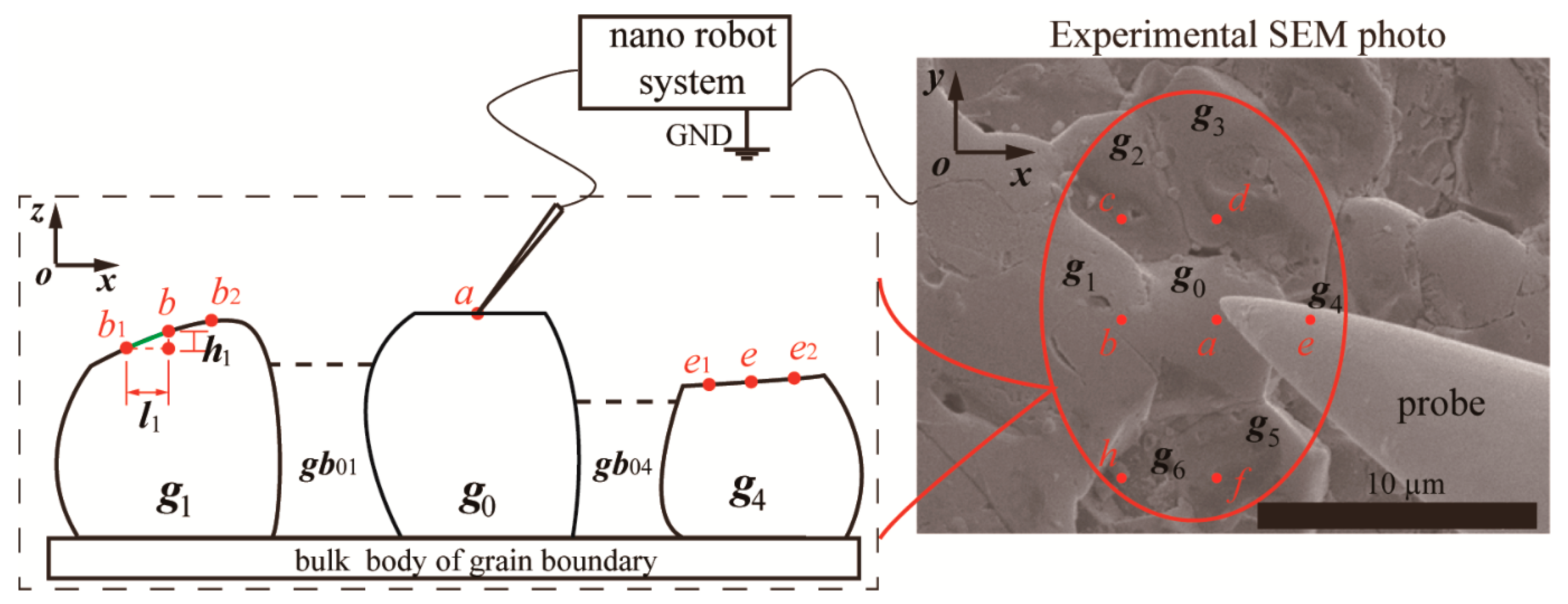
In order to accomplish the three-dimensional characterization of nonlinear grain boundary interface lengths in the micro-area of bulk ZnO, two-dimensional profile structure lengths of the targeted grain boundaries can be imaged in plane X-Y. Next, Z-directional heights in plane X-Z and plane Y-Z can be obtained by nanorobot probing at the equidistant positions. As illustrated in Figure 1, it is a schematic diagram accounting for three-dimensional characterization of nonlinear structure lengths of micro-area grain boundary interfaces in bulk ZnO ceramics. After two-dimensional structures of the targeted grain boundary had been imaged to quantify the profile lengths in plane X-Y. When Z-directional relative differences had been vertically probed between different positions, the nanorobot end tip needed to be detected to accomplish the real contact to the upper surface in plane X-Y. At this point, taking Z-directional height as the initial reference occurred.

Figure 1.
Schematic diagram accounting for three-dimensional characterization of nonlinear structure lengths of micro-area grain boundary interfaces in bulk ZnO ceramics.
In order to verify the rationality of nanorobot-based probing of Z-dimensional heights, six positions at micro-area grain boundaries consisted of the targeted grains g1, g2, g3, g4, g5, and g6 were taken as the Z-directional height probing points. Here, the nanorobot-based Z-directional heights probing of grain boundary g1-g0-g4 in plane X-Z was regarded as an example, seen from the dashed box in details. The probing positions b1, b, b2 and position e1, e, and e2 were individually selected as the sample probing positions on the adjacent grain g1 and grain g4 along the X direction, with a horizontal equidistance of 1 μm. Assuming that the distance l1 = 1 μm, Z-directional relative vertical height difference h1 can be acquired by probing position b and b1 in sequence. As a result, it can be deduced to obtain the hypotenuse length as a part of grain boundary using the trigonometric geometric relation assumed by magnification. Similarly, after the position b2 has been probed by the nanorobot, partial nonlinear grain boundary length, which can be regarded as a projected length with oblique angle of grain boundary interfacial layer, can be drawn by Z-dimensional heights at position b1, b, and b2. It is then reasonable to demonstrate that the probing process of Z-directional heights probed at g2-g0-g6 and g3-g0-g5 in plane Y-Z are similar with that in plane X-Z.
After the grain boundary profile data in plane X-Y were obtained, a model of irregular length can be visually reconstructed by software to realize a virtual stereoscopic intuition expression for the nonlinear length of inner grain boundary.
3. Results and discussion
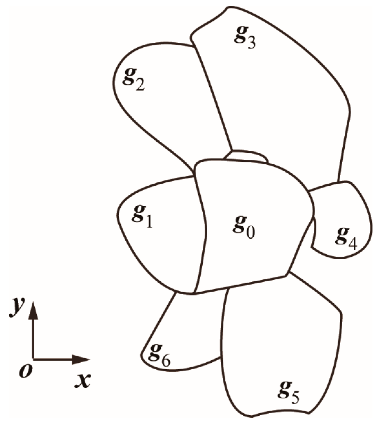
In order to establish three-dimensional structure morphologies of nonlinear grain boundaries, two-dimensional structures in plane X-Y need to be acquired first. After the targeted grain boundaries have been imaged by SEM, two-dimensional profile structure projections of multiple interface layers can be obtained in plane X-Y, as shown in Figure 2. It can be easily observed that grain boundary length structures projections in plane X-Y can be constructed by the targeted six grains, i.e., g1, g2, g3, g4, g5, and g6. Thus, relative positions away from the central grain g0 were uniquely identified at the two-dimensional plane. It can be apparent to demonstrate that profile structures of grain boundaries in the two-dimensional plane present the characteristics of irregular shapes and unequal lengths. However, two-dimensional profile structures may be simplified to different shapes composed by straight lines and arc shapes.

Figure 2.
Two-dimensional projections of the contour structure length of the grain boundary interface layer in plane X-Y.
It is worthy of note that it is an assumption to take the contour line of each grain to be considered as the relative uniform thickness of the grain boundary interface. In fact, the thickness of the grain boundary interface layer may vary in different orientations.
It can be further confirmed that grain boundary profile structures can be regarded as the nonlinear expression existing in a two-dimensional plane with irregular and unequal lengths. Furthermore, it can be envisioned that the grain boundary interface layer may exist nonlinearly in three dimensions.
In order to quantify the micromorphology of a grain boundary in plane X-Y, Z-directional height probing of the targeted grain positions along plane X-Z and plane Y-Z profiles can be performed using a nanorobot end probe.
As shown in Figure 3, Z-directional relative heights of three positions on adjacent grains can be individually probed by a nanorobot along plane X-Z and plane Y-Z profiles at equal distances. Figure 3a illustrates the projection drawing of Z-direction relative height differences of g1 and g4 relative to g0 along the X direction. Probing positions on g1 are individually represented as b1, b, and b2, and Lb1b = Lbb2 = 1 μm along the X direction. Additionally, probing positions on g4 are individually represented as e1, e, and e2, and Le1e = Lee2 = 1 μm along the X direction. Correspondingly, Figure 3b illustrates the projection drawing of Z-direction relative height differences of g2 and g6 relative to g0 along the Y direction. Probing positions on g2 are c1, c, and c2, where Lc1c = Lcc2 = 1 μm along the Y direction. Additionally, probing positions on g6 are h1, h, and h2, and where Lh1h = Lhh2 = 1 μm along the Y direction. Figure 3c illustrates the projection drawing of Z-direction relative height differences of g3 and g5 relative to g0 along the Y direction. Probing positions on g3 are d1, d, and d2, where Ld1d = Ldd2 = 1 μm along the Y direction. Additionally, probing positions on g5 are f1, f, and f2, where Lf1f = Lff2 = 1 μm along the Y direction.

Figure 3.
Z-directional relative heights of three positions on adjacent grains individually probed by nanorobot along plane X-Z and plane Y-Z profile at equal distances. (a) A projection drawing of Z-direction relative height differences of g1 and g4 relative to g0 along the X direction. (b) Projection drawing of Z-direction relative height differences of g2 and g6 relative to g0 along the Y direction. (c) Projection drawing of Z-direction relative height differences of g3 and g5 relative to g0 along the Y direction.
After local micro-area Z-directional micromorphology of the targeted grains in plane X-Y have been probed by nanorobot, Z-dimensional relative height differences at different probing positions can be obtained by comparing with grain g0. Specifically, viewed from Figure 3a, Z-directional relative height differences of three equidistant probing positions b1, b, b2 on g1 and e1, e, e2 on g4 relative to g0 are −2.3 μm, −2.1 μm, −2.0 μm, and −8.8 μm, −8.7 μm, −8.5 μm, respectively. Viewed from Figure 3b, Z-directional relative height differences of three equidistant probing positions c1, c, c2 on g2 and h1, h, h2 on g6 relative to g0 are −6.8 μm, −6.9 μm, −7.0 μm and −3.56 μm, −3.5 μm, −3.44 μm, respectively. Viewed from Figure 3c, Z-directional relative height differences of three equidistant probing positions d1, d, d2 on g3 and f1, f, f2 on g5 relative to g0 are −5.0 μm, −5.2 μm, −5.4 μm and −2.86 μm, −2.9 μm, and −2.93 μm, respectively. Consequently, Z-directional relative height differences at the local grain boundary interface in plane X-Y can be drawn by nanorobot probing at the same equidistant positions on each grain surface.
Viewed from height data obtained by nanorobot Z-directional probing of different positions in plane X-Y, grain boundary lengths can present irregular and non-flat conditions, possessing unequal expressions along three-dimensional directions. Grain boundary lengths in plane X-Y, constructed by grains g1, g4, and g6 away from the targeted grain g0, present a trend of relatively gradually increasing behavior. On the contrary, grain boundary lengths constructed by grains g2, g3, and g5 present a trend of relatively gradually decreasing behavior. By performing Z-directional nano-probing of adjacent grain surfaces, it is demonstrated that grain shapes can be regarded as irregular characteristics. As a result, three-dimensional nonlinear grain boundaries can also be verified. This method proves that it is effective to characterize three-dimensional length structures of nonlinear polycrystalline grain boundaries using a nanorobot in SEM. It can also make up for the nonlinear morphologies of three-dimensional grain boundaries in bulk ZnO.
Furthermore, SEM imaging combined with robotic Z-directional nano-probing can be utilized to exhibit different internal topographical features of three-dimensional grain boundaries in a micro area of bulk ZnO. Furthermore, it can be used to guide the improvement of composition proportion and synthesis process of bulk ZnO so as to achieve the purpose of improving the macroscopic properties of bulk ZnO by constructing three-dimensional grain boundary morphology.
Correspondingly, a map of local nonlinear lengths of different grain boundary interface layers can be virtually reconstructed, as illustrated in Figure 4. Obviously, the grain boundary interface layer length of each grain possesses a different counter shape. Therefore, it can be deduced that the irregular nonlinear grain boundary length may play a key role in the expression of macro conductance characteristics, which can extend the influences of grain boundary thickness along the depth direction. It is further verified from a nonlinear virtual reconstruction map that an approach of SEM coupled with nanorobots for characterization of micro-area grain boundary lengths is feasible. A virtual reconstruction of the local micro-area of three-dimensional grain boundary length structures can be adopted to interpret the nonlinear electrical characteristics expression of macro bulk polycrystalline ZnO.

Figure 4.
Virtual reconstruction map of local nonlinear lengths of grain boundary interface layers.
It is worth emphasizing that relative heights probed individually along plane X-Z and plane Y-Z can be further utilized to illustrate nonlinear height differences of grain boundary interface lengths. It is further envisioned that if all of the real relative heights of grain boundary interfaces could be quantitatively probed using a nanorobot in plane X-Y, nonlinear grain boundary lengths may be theoretically virtually reconstructed in details. Furthermore, the method can be advanced to accomplish three-dimensional lengths division of grain boundaries, which can potentially provide a unique way to realize the nonlinear mapping characterization of grain boundary length and electrical properties.
Additionally, this proposed method can be utilized to try to address the technological difficulties using isometric brick divisions of grain boundaries. Furthermore, the method can also obtain nonlinear quantitative topographies to divide grain boundaries to uneven structure in property analysis of bulk polycrystalline materials.
As for potential applications, this proposed characterization method can be further utilized to guide a technical improvement of polycrystalline materials synthesis, which can have positive effects on the material composition ratio and processing technology.
4. Conclusions
Aiming at the problem of lack of three-dimensional morphology for nonlinear characterization of a grain boundary to address isometric brick divisions, an approach of three-dimensional length characterization of grain boundary morphology can be proposed under SEM using a nanorobot to accomplish local micro-area nonlinear structure characterization in bulk polycrystalline ZnO. Experiments demonstrate that it is feasible for structure characterization and the reconstruction of the nonlinear length of three-dimensional grain boundaries in bulk materials. It can be further confirmed that grain boundary profile structures can be regarded as the nonlinear expression existing in a two-dimensional plane with irregular and unequal lengths. Nanorobot-based micro-area Z-dimensional relative vertical differences can be utilized to verify that nonlinear and irregular structure characteristics exist in bulk materials. They can also make up for the nonlinear morphologies of three-dimensional grain boundaries in bulk ZnO. It can be deduced that the irregular nonlinear grain boundary length may play a key role in the expression of macro conductance characteristics, which can extend the influences of grain boundary thickness along the depth direction. Virtual reconstruction of local micro-area grain boundary length structures can be adopted to interpret the nonlinear electrical characteristics expression of macro bulk polycrystalline ZnO. Furthermore, it can be advanced to accomplish three-dimensional lengths division of grain boundaries, which can potentially provide a unique way to realize the nonlinear mapping characterization of grain boundary length and electrical properties.
Author Contributions
Conceptualization, N.C., H.L., Z.W., S.X. and J.L.; Data curation, F.S. and N.C.; Investigation, Methodology, F.S., N.C., H.L. and S.X.; Supervision, H.L. and S.X.; Writing—original draft F.S.; Visualization, Writing—review & editing, N.C., H.L. and J.L. All authors have read and agreed to the published version of the manuscript.
Funding
This research was funded by the National Natural Science Foundation of China, grant number 61991415, 61827812, 62073209 and the Key Science and Technology Research Project of Henan Province, China, grant number 222102220032, 212102210359.
Data Availability Statement
Not applicable.
Conflicts of Interest
The authors declare that they have no conflict of interest.
References
- Kaufmann, B.; Billovits, T.; Supancic, P. Observation of an electrical breakdown at ZnO schottky contacts in varistors. J. Eur. Ceram. Soc. 2021, 41, 1969–1974. [Google Scholar] [CrossRef]
- Bueno, P.R.; Varela, J.A.; Longo, E. Admittance and dielectric spectroscopy of polycrystalline semiconductors. J. Eur. Ceram. Soc. 2007, 27, 4313–4320. [Google Scholar] [CrossRef]
- Kaufmann, B.; Raidl, N.; Supancic, P. Investigation of schottky barriers at Pd-ZnO junctions in varistors. J. Eur. Ceram. Soc. 2020, 40, 3771–3775. [Google Scholar] [CrossRef]
- Bremecker, D.; Keil, P.; Gehringer, M.; Isaia, D.; Rödel, J.; Frömling, T. Mechanically tuned conductivity at individual grain boundaries in polycrystalline ZnO varistor ceramics. J. Appl. Phys. 2020, 127, 034101. [Google Scholar] [CrossRef]
- Ivetić, T.B.; Sekulić, D.L.; Papan, J.; Gúth, I.O.; Petrović, D.M.; Lukić-Petrović, S.R. Niobium and zinc doped titanium-tin-oxide solid-solution ceramics: Synthesis, structure and electrical characterization. Ceram. Int. 2018, 44, 18987–18995. [Google Scholar] [CrossRef]
- Buono, C.; Uriz, A.J.; Aldao, C.M. Effects of intergranular capacitance and resistance dispersion on polycrystalline semiconductor impedance. Solid State Ion. 2019, 343, 115076. [Google Scholar] [CrossRef]
- Nevosad, A.; Hofstätter, M.; Supancic, P.; Danzer, R.; Teichert, C. Micro four-point probe investigation of individual ZnO grain boundaries in a varistor ceramic. J. Eur. Ceram. Soc. 2014, 34, 1963–1970. [Google Scholar] [CrossRef]
- Fleig, J.; Rodewald, S.; Maier, J. Microcontact impedance measurements of individual highly resistive grain boundaries: General aspects and application to acceptor-doped SrTiO3. J. Appl. Phys. 2000, 87, 2372–2381. [Google Scholar] [CrossRef]
- Rodewald, S.; Fleig, J.; Maier, J. Microcontact impedance spectroscopy at single grain boundaries in Fe-Doped SrTiO3 polycrystals. J. Am. Ceram. Soc. 2001, 84, 521–530. [Google Scholar] [CrossRef]
- Shao, R.; Kalinin, S.V.; Bonnell, D.A. Local impedance imaging and spectroscopy of polycrystalline ZnO using contact atomic force microscopy. Appl. Phys. Lett. 2003, 82, 1869–1871. [Google Scholar] [CrossRef]
- Cao, N.; Xie, S.R.; Li, H.Y.; Yang, Y.; Liu, N.; Liu, M.; Pu, H.Y.; Luo, J.; Gong, Z.B. Micro-nano manipulator based localized micro-area electrical impedance measurement for polycrystalline ZnO in scanning electron microscope. Mater. Lett. 2018, 219, 273–275. [Google Scholar] [CrossRef]
- Cao, N.; Shen, F.L. In-situ mapping characterization of structure and electrical property of grain boundary in polycrystalline ZnO using nanorobot in SEM. Ceram. Int. 2022, in press. [CrossRef]
- Shen, F.L.; Cao, N.; Li, H.Y.; Xie, S.R. Structure characterization of interior invisible single grain boundary by nanorobot pick-and-place grain in bulk ZnO under SEM. Mater. Lett. 2022, 324, 132777. [Google Scholar] [CrossRef]


Publisher’s Note: MDPI stays neutral with regard to jurisdictional claims in published maps and institutional affiliations. |
© 2022 by the authors. Licensee MDPI, Basel, Switzerland. This article is an open access article distributed under the terms and conditions of the Creative Commons Attribution (CC BY) license (https://creativecommons.org/licenses/by/4.0/).