


Investigation of Facetted Growth in Heavily Doped Silicon Crystals Grown in Mirror Furnaces

Abstract
:1. Introduction
2. Some Theoretical Considerations
2.1. Jackson Factor
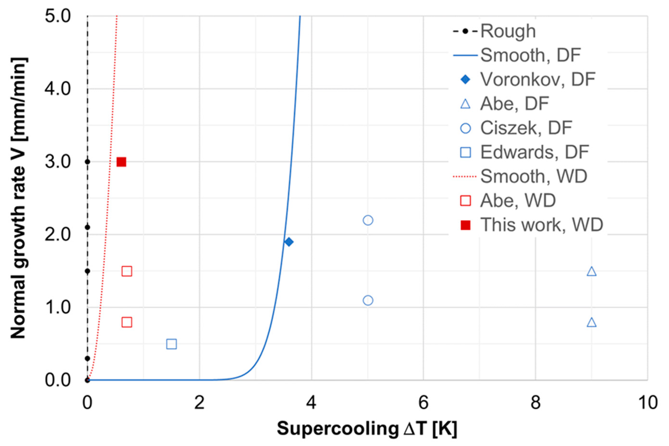
2.2. Growth Laws
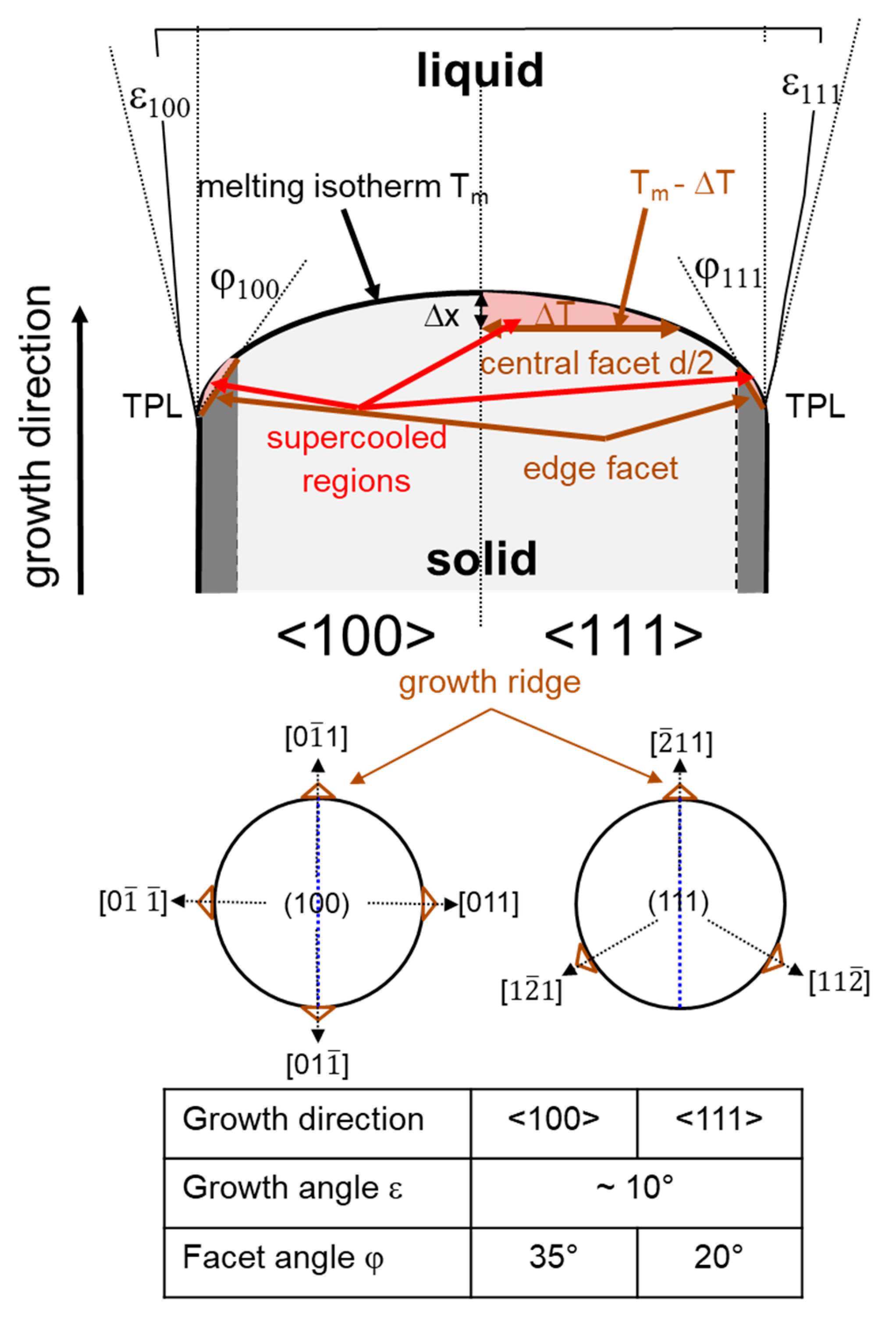
2.3. Crystallographic Aspects
2.4. Morphological Stability at High Dopant Concentrations
3. Experimental Details
4. Results and Discussion
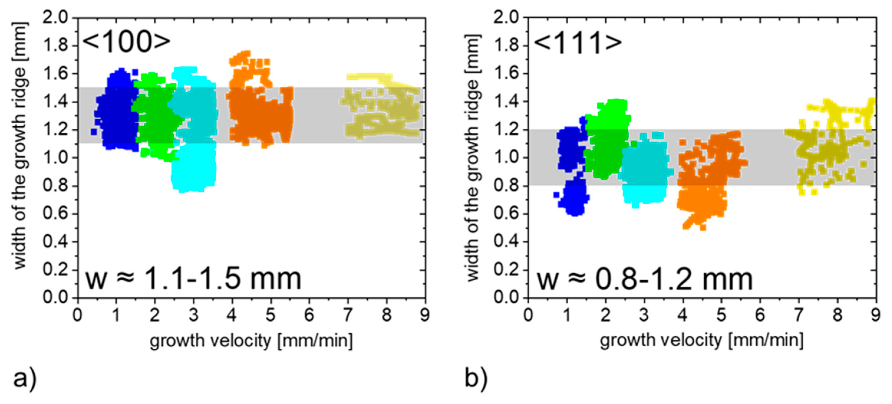
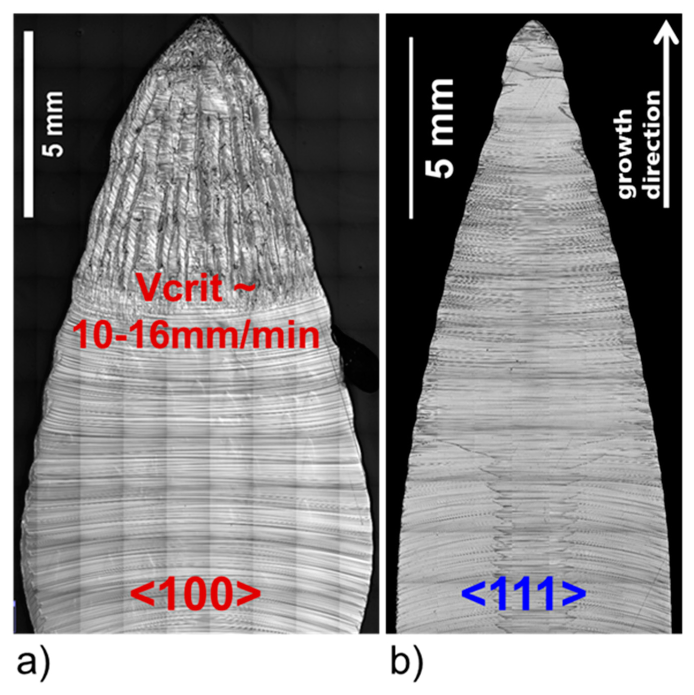
4.1. Growth Ridge Geometry for <100> and <111> Crystal Orientations
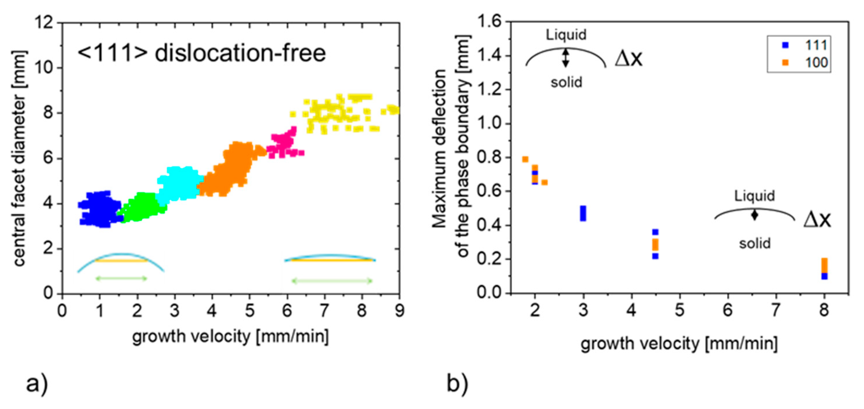
4.2. Diameter of the Central Facet
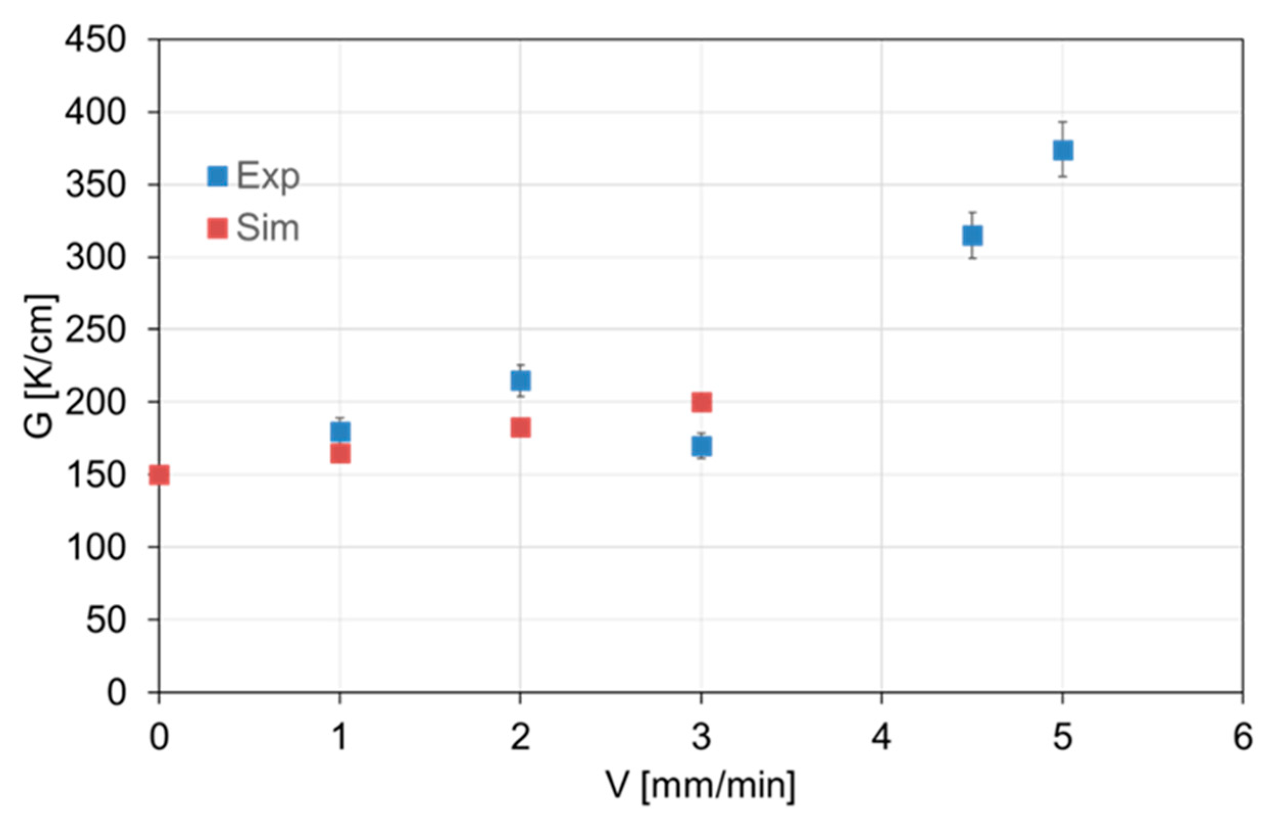
4.3. Morphological Instability
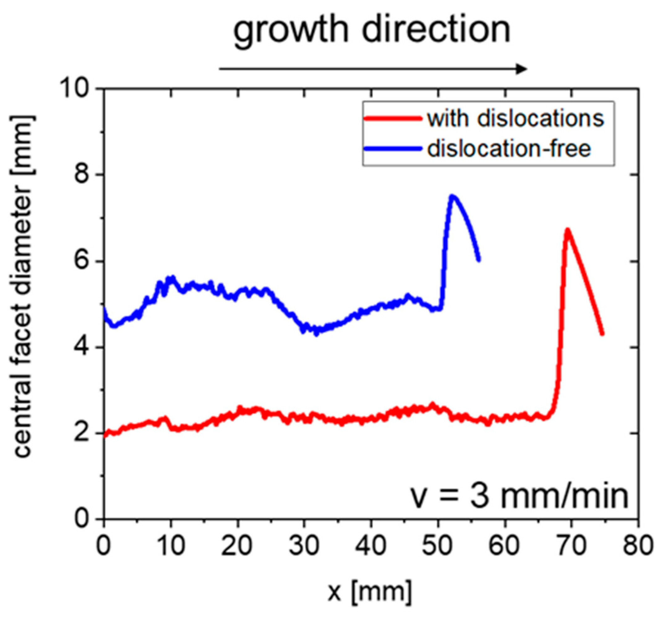
4.4. Fluctuations of the Central Facet
5. Conclusions
Author Contributions
Funding
Data Availability Statement
Conflicts of Interest
References
- Chernov, A.A. Stability of faceted shapes. J. Cryst. Growth 1974, 24–25, 11–31. [Google Scholar] [CrossRef]
- Weinstein, O.; Virozub, A.; Miller, W.; Brandon, S. Modeling anisotropic shape evolution during Czochralski growth of oxide single crystals. J. Cryst. Growth 2019, 509, 71–86. [Google Scholar] [CrossRef]
- Jurisch, M.; Eichler, S.; Bruder, M. Vertical Bridgman Growth of Binary in Compound Semiconductors. In Handbook of Crystal Growth; Nishinga, T., Rudolph, P., Kuech, T., Eds.; Elsevier: Amsterdam, The Netherlands, 2015; pp. 331–372. [Google Scholar]
- Chen, T.P.; Chen, F.R.; Chuang, Y.C.; Guo, Y.D.; Peng, J.G.; Huang, T.S.; Chen, L.J. Study of twins in GaAs, GaP and InAs crystals. J. Cryst. Growth 1992, 118, 109–116. [Google Scholar] [CrossRef]
- Koh, H.; Choi, M.; Park, I.; Fukuda, T. Twins in GaAs crystals grown by the vertical gradient freeze technique. Cryst. Res. Technol. 1995, 30, 397–403. [Google Scholar] [CrossRef]
- Chung, H.; Dudley, M.; Larson, D., Jr.; Hurle, D.; Bliss, D.; Prasad, V. The mechanism of growth-twin formation in zincblende crystals: New insights from a study of magnetic liquid encapsulated Czochralski-grown InP single crystals J. Cryst. Growth 1998, 187, 9–17. [Google Scholar] [CrossRef]
- Antonov, V.; Elsakov, V.; Olkhovikova, T.; Selin, V. Dislocations and 90°-twins in LEC-grown InP crystals. J. Cryst. Growth 2002, 235, 35–39. [Google Scholar] [CrossRef]
- Voronkov, V.V. Supercooling on the face arising at the rounded front of crystallization,” Kristallografiya. Kristallografiya 1972, 17, 909–917. [Google Scholar]
- Voronkov, V.V. Processes at the boundary of a crystallization front. Kristallografiya 1974, 19, 922–929. [Google Scholar]
- Voronkov, V.V. Mass transfer on the crystal surface near the melt boundary and its effect on the shape of the growing crystal. Kristallografiya 1978, 23, 249–256. [Google Scholar]
- Voronkov, V.V. Faceting of crystals pulled from the melt. Izvestiya Akademii Nauk SSSR. Seriya Fizicheskaya 1983, 47, 210–218. [Google Scholar]
- Voronkov, V.V. Effects of facets at the crystallization front on crystal shape. Izvestiya Akademii Nauk SSSR. Seriya Fizicheskaya 1985, 49, 2467–2472. [Google Scholar]
- Brice, J.C. Facet formation during crystal pulling. J. Cryst. Growth 1970, 6, 205–206. [Google Scholar] [CrossRef]
- Pirnia, A.; Helenbrook, B.T. Physics of double faceted crystal growth in solidification processes. J. Cryst. Growth 2022, 555, 1259558. [Google Scholar] [CrossRef]
- Stamelou, V.; Tsoutsouva, M.G.; Riberi-Beridot, T.; Reinhart, G.; Regula, G.; Baruchel, J.; Mangelinck-Noël, N. {111} facet growth laws and grain competition during silicon crystallization J. Cryst. Growth 2017, 479, 1–8. [Google Scholar] [CrossRef] [Green Version]
- Sabanskis, A.; Bergfelds, K.; Muiznieks, A.; Schröck, T.; Krauze, A. Crystal shape 2D modeling for transient CZ silicon crystal growth. J. Cryst. Growth 2013, 377, 9–16. [Google Scholar] [CrossRef]
- Krauze, A.; Virbulis, J.; Zitzelsberger, S.; Ratnieks, G. 3D modeling of growth ridge and edge facet formation in <100> floating zone silicon crystal growth process. J. Cryst. Growth 2019, 520, 68–71. [Google Scholar] [CrossRef]
- Kearns, J.K. Origin of Growth Twins during Czochralski Growth of Heavily Doped, Dislocation-Free Single Crystal Silicon. Ph.D. Thesis, Worcester Polytechnic Institute, Worcester, MA, USA, 2019. Available online: https://digitalcommons.wpi.edu/etd-dissertations/514 (accessed on 3 November 2022).
- Stockmeier, L.; Kranert, C.; Fischer, P.; Epelbaum, B.; Reimann, C.; Friedrich, J.; Raming, G.; Miller, A. Analysis ot he geometry ot he growth ridges and correlation ot he thermal gradient during growth of silicon crystals by the Czochralski-method. J. Cryst. Growth 2019, 515, 26–31. [Google Scholar] [CrossRef]
- Kranert, C.; Raming, G.; Miller, A.; Reimann, C.; Friedrich, J. Facet growth and geometry of the growth ridge during dynamic Czochralski processes J. Cryst. Growth 2021, 568–569, 126174. [Google Scholar] [CrossRef]
- Abe, T. The growth of Si single crystals from the melt and impurity incorporation mechanisms. J. Cryst. Growth 1974, 24–25, 463–467. [Google Scholar] [CrossRef]
- Stockmeier, L.; Lehmann, L.; Miller, A.; Reimann, C.; Friedrich, J. Dislocation formation in heavily As-doped Czochralski grown silicon. Cryst. Res. Technol. 2017, 1600373, 1–6. [Google Scholar] [CrossRef]
- Taishi, T.; Ohno, Y.; Yonenaga, I. Constitutional supercooling in heavily As-doped Czochralski Si crystal growth. J. Cryst. Growth 2014, 393, 42–44. [Google Scholar] [CrossRef] [Green Version]
- Kossel, W. Zur Theorie des Kristallwachstums. Nachr. Ges. Wiss. Gott. 1927, 135–143. [Google Scholar]
- Stranski, I.N. Zur Theorie des Kristallwachstums. Z. Phys. Chem. 1928, 136, 259. [Google Scholar] [CrossRef]
- Jackson, K. Actual Concepts of Interface Kinetics, in Crystal Growth—From Fundamentals to Technology; Müller, G., Metois, J.J., Rudolph, P., Eds.; Elsevier: Amsterdam, The Netherlands, 2004; pp. 27–53. [Google Scholar]
- Miller, W. Some remarks on the undercooling of the Si(1 1 1) facet and the “Monte Carlo modeling of silicon crystal growth” by Kirk M. Beatty & Kenneth A. Jackson, J. Crystal Growth 211 (2000) 13. J. Cryst. Growth 2011, 325, 101–103. [Google Scholar]
- Mullins, W.W.; Sekerka, R.F. Stability of a Planar Interface during Solidification of a Dilute Binary Alloy. J. Appl. Phys. 1964, 35, 444–451. [Google Scholar] [CrossRef]
- Holmes, D.E.; Gatos, H.C. Morphological stability of the planar solid-liquid interface J. Appl. Phys. 1981, 52, 2971–2982. [Google Scholar] [CrossRef]
- Bardsley, W.; Boulton, J.S.; Hurle, D.T.J. Constitutional supercooling during crystal growth from stirred metls: III. The morphology of the germanium cellular structure. Solid-State Electron. 1962, 5, 395–403. [Google Scholar] [CrossRef]
- Tiller, W.A.; Jackson, K.A.; Rutter, J.W.; Chalmers, B. The Redistribution of Solute Atoms during the Solidification of Metals. Acta Metall. 1953, 1, 428–437. [Google Scholar] [CrossRef]
- Hurle, D.T.J. Constitutional supercooling during crystal growth from stirred melts. I Theoretical. Solid Sate Electron. 1961, 3, 37–44. [Google Scholar] [CrossRef]
- Pfann, W.G. Zone Melting; Wiley: New York, NY, USA, 1958. [Google Scholar]
- Eyer, A.; Cröll, A.; Nitsche, R. Floating zone growth of silicon under microgravity in a sounding rocket. J. Cryst. Growth 1985, 71, 173–182. [Google Scholar] [CrossRef]
- Dold, P.; Benz, K.W.; Cröll, A.; Roux, B.; Lyubimov, D.; Lyubimova, T.; Scuridyn, R. Vibration controlled convection – preparation and perspective of the Maxus 4 experiment. Acta Astronaut. 2001, 48, 639–646. [Google Scholar] [CrossRef]
- Cröll, A.; Dold, P.; Kaiser, T.; Szofran, F.R.; Benz, K.W. The Influence of Static and Rotating Magnetic Fields on Heat and Mass Transfer in Silicon Floating Zones. J. Electrochem. Soc. 1999, 146, 2270–2275. [Google Scholar] [CrossRef]
- Dash, W.C. Silicon Crystals Free of Dislocations. J. Appl. Phys. 1958, 29, 736. [Google Scholar] [CrossRef]
- Friedrich, J.; Müller, G. Crystal Growth, Bulk: Methods. In Encyclopedia of Condensed Matter Physics; Bassani, F., Liedl, G.L., Wyder, P., Eds.; Elsevier: Amsterdam, The Netherlands, 2005; pp. 262–274. [Google Scholar]
- Cröll, A.; Müller, W.; Nitsche, R. Floating-zone growth of surface-coated silicon under microgravity J. Growth 1986, 79, 65–70. [Google Scholar] [CrossRef]
- Friedrich, J.; Reimann, C.; Jauss, T.; Cröll, A.; Sorgenfrei, T. Interaction of SiC particles with moving solid-liquid interface during directional solidification of silicon J. Cryst. Growth 2016, 447, 18–26. [Google Scholar] [CrossRef]
- Sorgenfrei, T.; Jauß, T.; Friedrich, J.; Reimann, C.; Cröll, A. The Critical Growth Rate for Particle Incorporation during the Directional Solidification of Solar Silicon under Microgravity. Int. J. Microgravity Sci. Appl. 2017, 34, 340115. [Google Scholar]
- Hürner, S.; Friedrich, J. Public Final Report of the InSituKris-Project founded by DLR under FKZ 50WM1757. 2020. At German National Library of Science and Technology. Available online: https://edocs.tib.eu/files/e01fb22/1801198268.pdf (accessed on 3 November 2022).
- Voronkov, V.V.; Dai, B.; Kulkarni, M.S. Fundamentals and Engineering of the Czochralski Growth of Semiconductor Silicon Crystals. Compr. Semicond. Sci. Technol. 2011, 3, 81–169. [Google Scholar]
- Dikhoff, J.A.M. Cross-sectional resistivity variations in germanium single crystals. Solid-State Electron. 1960, 1, 202–210. [Google Scholar] [CrossRef]
- Baumgartl, J.; Budweiser, W.; Müller, G.; Neumann, G. Studies of buoyancy-driven convection in a vertical cylinder with parabolic temperature profile. J. Cryst. Growth 1989, 97, 9–17. [Google Scholar] [CrossRef]


| Material | ΔS/k | η/Z (100) | η/Z (111) | α{100} | α{111} |
|---|---|---|---|---|---|
| Si | 3.6 | 1/2 | 3/4 | 1.8 (r) | 2.7 (s) |
| GaAs | 7.4 | 1/2 | 3/4 | 3.7 (r) | 5.6 (s) |
| InP | 5.6 | 1/2 | 3/4 | 2.8 (r) | 4.2 (s) |
| CdTe | 4.4 | 1/2 | 3/4 | 2.2 (r) | 3.3 (s) |
Publisher’s Note: MDPI stays neutral with regard to jurisdictional claims in published maps and institutional affiliations. |
© 2022 by the authors. Licensee MDPI, Basel, Switzerland. This article is an open access article distributed under the terms and conditions of the Creative Commons Attribution (CC BY) license (https://creativecommons.org/licenses/by/4.0/).
Share and Cite
Gruner, S.; Kranert, C.; Jauß, T.; Sorgenfrei, T.; Reimann, C.; Friedrich, J. Investigation of Facetted Growth in Heavily Doped Silicon Crystals Grown in Mirror Furnaces. Crystals 2022, 12, 1575. https://doi.org/10.3390/cryst12111575
Gruner S, Kranert C, Jauß T, Sorgenfrei T, Reimann C, Friedrich J. Investigation of Facetted Growth in Heavily Doped Silicon Crystals Grown in Mirror Furnaces. Crystals. 2022; 12(11):1575. https://doi.org/10.3390/cryst12111575
Chicago/Turabian StyleGruner, Sebastian, Christian Kranert, Thomas Jauß, Tina Sorgenfrei, Christian Reimann, and Jochen Friedrich. 2022. "Investigation of Facetted Growth in Heavily Doped Silicon Crystals Grown in Mirror Furnaces" Crystals 12, no. 11: 1575. https://doi.org/10.3390/cryst12111575