Article

Promoting Light Extraction Efficiency of Ultraviolet Light Emitting Diodes by Nanostructure Optimization

1
School of Materials Science and Engineering, Jiangsu University, Zhenjiang 212013, China
2
Zhejiang Provincial Engineering Research Center of Energy Optoelectronic Materials and Devices, Ningbo Institute of Materials Technology and Engineering, Chinese Academy of Sciences (CAS), Ningbo 315201, China
*
Authors to whom correspondence should be addressed.
Crystals 2022, 12(11), 1601; https://doi.org/10.3390/cryst12111601
Submission received: 21 October 2022 / Revised: 3 November 2022 / Accepted: 7 November 2022 / Published: 10 November 2022
(This article belongs to the Special Issue Preparation and Characterization of Optoelectronic Functional Films)

Abstract

:
Ultraviolet (UV) light-emitting diodes (LEDs), as one of the more promising optoelectronic devices, are intrinsically limited by poor light extraction efficiencies (LEEs). To unlock the full potential of UV-LEDs, we propose a simple and effective strategy to promote the LEEs of UV-LEDs by screening and tailoring suitable optical structures/designs through rigorous numerical simulations. The photonic crystals (PCs) and/or nano-patterned sapphire substrates (NPSSs) equipped with the nano-pillar, nano-cone, nano-oval, and their derivates, are particularly investigated. The simulated results show that individual PC with an average transmittance of 28% is more efficient than that of individual NPSS (24.8%). By coupling PC and NPSS structures, a higher LEE with an average transmittance approaching 29% is obtained, much higher than that of the flat one (23.6%). The involved mechanisms are clarified and confirm that the promotion of optical performance of the nanostructured devices should be attributed to the widened response angles (from 0 to 60°), rather than the enhanced transmittances in the small angles within 30°.

1. Introduction

Ultraviolet (UV) light-emitting diodes (LEDs) based on group III-nitrides, especially AlGaN, have gained increasing attention in the fields of water purification, sterilization, sensing, and plant lighting, etc., owing to their remarkable advantages of long lifetime, low power consumption, and the environmentally-friendly nature of the solid-state light source [1,2,3,4,5,6,7]. External quantum efficiency (EQE) produced from a combination of internal quantum efficiency (IQE) and light extraction efficiency (LEE) is a key indicator to evaluate the performance of UV-LEDs. It is, therefore, of great importance to increase EQEs to unlock the full potential of UV LEDs. However, the most reported EQEs of UV-LEDs are generally below 10%, much lower than that of their mainstream blue LED counterparts [8,9,10,11,12,13,14]. Advanced fabrication methods and designs have been intensively adopted and/or integrated to improve the crystal quality of AlxGa1-xN films, endowing a high IQE with the value exceeding 90% for the AlGaN-based UV-LEDs [15,16,17,18,19,20]. This means that the performance of UV-LEDs is intrinsically limited by the LEEs, rather than IQEs.
Generally, the poor LEEs can be attributed to the strong parasitic absorption of p-type GaN films, the undesired transverse magnetic (TM) polarization due to enhanced Al composition in the AlGaN multiple-quantum-wells (MQWs), together with the mismatched impedance between III-nitride and sapphire/air [2,21]. The first issue can be partially remitted by the regulation and modification of the related materials but usually at the expense of lowering IQEs. The high TM/TE light polarization ratio is an intrinsic nature of UV-LED, and can be modulated by controlling the strain state of the MQWs. The last one (i.e., the mismatched impedance) can be alleviated by the advanced optical designs, which are also considered to be a more efficient scheme to promote the LEEs and the EQEs of UV-LEDs. To address this issue, a great number of strategies including MQWs with nanostructured arrays [22,23,24,25], nano-patterned sapphire substrates (NPSSs) [26,27,28,29,30], photonic crystals (PCs) [31,32], etc., have been implemented. For instance, Guo et al. reported nanostructured MQWs textured with nanopillar or nanohole arrays by using a polystyrene sphere mask coupled with reactive-ion-etching (RIE) technology, demonstrating an improved performance with photoluminescence (PL) integral intensities for the nanopillar/nanohole structured devices are 8.01/4.06 times that of the flat counterpart [22]. Djavid et al. proposed a deep UV-LED featuring nanowire structures to promote the LEEs of TM polarized light in the lateral side emission, and numerically predicted a high LEE of 72% under the optimized structure designs [23]. Even though texturing MQWs with nanostructures is conducive to boosting the LEEs of UV-LEDs, the related electrical performance and the IQEs will be degraded due to the introduction of more defects during the fabrication of the nanostructured MQWs [22]. As a contrast, NPSS and PC structures could also provide excellent optical management without sacrificing electrical performance [27,32]. In addition, NPSS could relieve or release the stresses in the subsequent film deposition process and thus improve the film quality [33]. Dong et al. fabricated UV LEDs featuring NPSS structures by using UV light exposure and wet etching technology, showing an enhanced device performance with an EQE value of 3.45% [26]. Wang et al. introduced a moth-eye PC structure into UV-LEDs, which could effectively enhance light output power compared with the flat counterpart [32]. Zheng et al. proposed a double nano-pattern on the sapphire substrates, i.e., the nano-cone structures coated with the nano-structured fluoropolymer resin PCs, yielding a high light output power of 28.3% [11]. Additionally, Ooi et al. numerically investigated the microdome NPSS and PC structures for UV-LEDs and concluded that this type of design is predominantly beneficial in enhancing TM polarized output [34]. Although NPSS and PC structures have been widely confirmed to be conducive to the LEEs of UV-LEDs, their potential has not been fully explored yet. Moreover, the interplay between NPSS and PC structures towards the development of higher efficiency UV-LEDs is still not clear in the community.
Here, we propose a strategy to promote the LEEs of UV-LEDs by screening a large number of optical structures to build PCs, NPSSs, and their combinations. By implementing the rigorous numerical simulations, PCs and NPSSs equipped with the representative nanopillar, nano-cone, nano-oval, and their derivates, are investigated. The simulated results suggest that the introduction of PCs and NPSSs could boost the LEEs of UV-LEDs compared with the flat counterpart, in which devices with nano-cone configurations could achieve the highest LEEs. In terms of the LEEs, the individual PC designs are considered more efficient than the individual NPSSs, which, however, can be partially compensated by modifying refractive indexes of the NPSS interspace. Moreover, the angle-dependent transmittance curves point out that the improvement of the average transmittances due to PC or NPSS designs mainly comes from the expansion of critical angles other than the enhancement of the transmittances at small angles. The spatial electric-field distributions are also presented to address the related mechanisms of optical response, confirming that the improved optical performance in the large angles can be attributed to the change of direction of the incident light by inducing the high-order resonance modes.

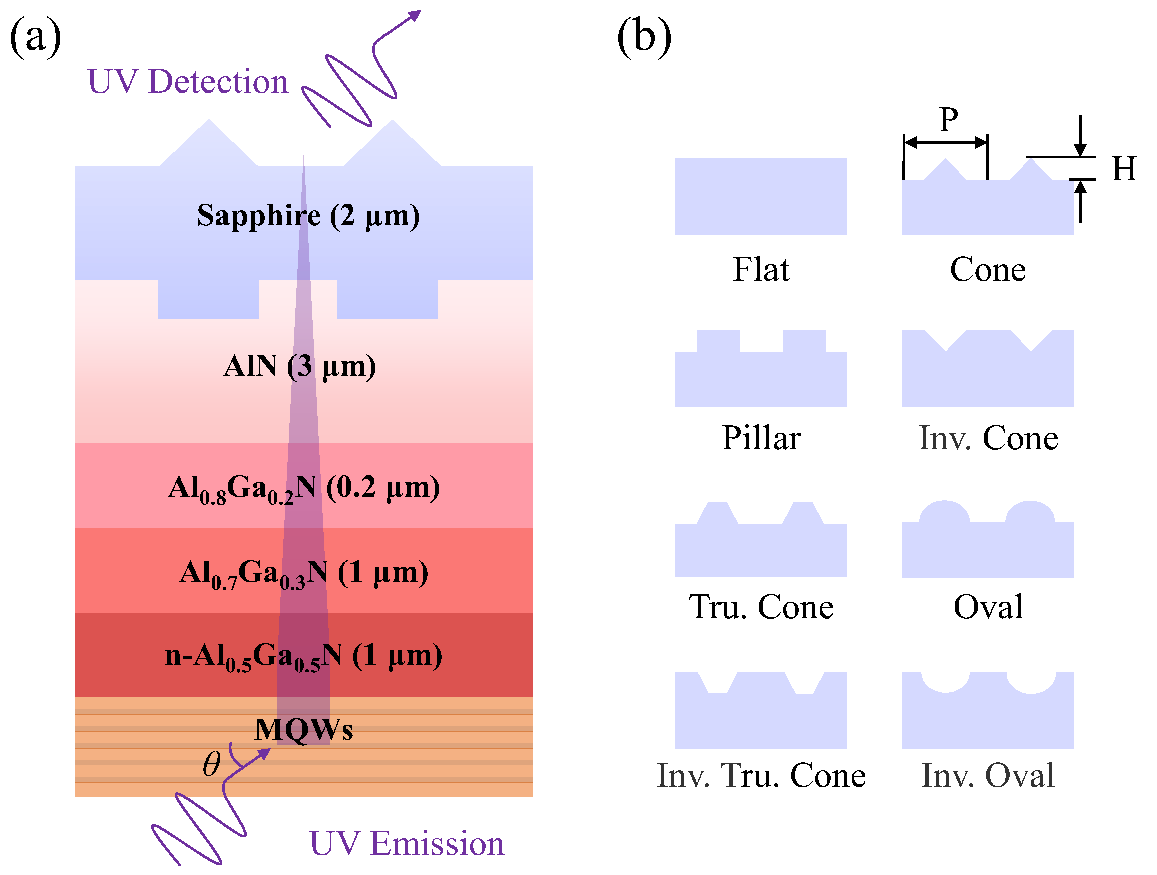
2. Model and Simulation Methods

Figure 1a shows the simulated structure of UV LEDs, which is composed of a 2 μm thick sapphire substrate, a 3 μm thick AlN buffer layer, a 200 nm thick Al0.8Ga0.2N layer, a 1 μm thick Al0.7Ga0.3N, a 1 μm thick Al0.5Ga0.5N, and an MQW, where the Al0.8Ga0.2N and Al0.7Ga0.3N buffer layers are necessary to ensure the high-quality n-type Al0.5Ga0.5N films. Moreover, a series of nanopatterns including nano-cone, nano-pillar, nano-oval, truncated nano-cone (Tru. Cone), and their derived structures together with the flat counterpart are illustrated in Figure 1b. These patterned structures near and far from the AlN layers are defined as NPSSs and PCs, respectively. The period size, filling factor, and height of the nanopatterns are defined as P, ff, and H, respectively.
Here, the finite element simulations were implemented by solving the Maxwell’s equations based on the platform of COMSOL Multiphysics. The based equation is demonstrated as follows:
  ×   (   ×   E   )     k 0 2 ε r E = 0  
where E is the electric-field intensity, k0 is the wave number of free space, and εr is the relative dielectric constant. By solving this equation, the electric-field distributions within devices can be obtained, and the optical performance including frequency-dependent absorption, reflection, and transmittance, can be thus extracted. The optical parameters of the involved materials including refractive indexes were extracted from literature [35,36]. The bottom and top boundaries were decorated by the perfect match layers (PMLs) whose thicknesses were fixed at 300 nm to limit the calculation region. The periodic boundaries in the lateral directions were adopted to minimize the calculation workload. A planar light source with a fixed wavelength of 280 nm and an incident angle of θ was employed for this simulation. It is worth noting that the power emitted from the light source is assumed to be the same in any direction, and the referenced transmittance value is an average collected from all emitted angles. This treatment may be different from the actual one, but it is still of reference value for evaluating the overall performance.

3. Results and Discussion

3.1. Light Extraction of PC Patterns

Firstly, the LEEs of the UV-LEDs with PC structures were investigated, as shown in Figure 2. Here, three typical PC structures, i.e., nano-cone, nano-oval, and truncated nano-cone, were considered. After careful observation, we can conclude from Figure 2a–c that: (1) the three related cases (i.e., nano-cone, nano-oval, and truncated nano-cone) have similar dispersion characteristics, where the average transmittance (Tra.) plateaus were marked by the black dotted lines; (2) UV-LED with PC-Cone has a slightly higher maximum Tra. value (~28%) than that of PC-Oval (~27%) and PC-Tru. Cone (~27.5%) cases; (3) H and P need to match each other to achieve the best optical response. In order to further optimize the optical performance of Tru. Cone structures, the relationship between structural parameters of fftop and ffbottom of Tru. Cone on Tra. was shown in Figure 2d, where the fftop and ffbottom are defined as the fill factors of top- and bottom-sizes. The detailed simulated results indicate that the best optical response occurs at fftop = 0 and ffbottom = 1, suggesting that as the PC structures for UV-LEDs, the nano-cone is better than the truncated nano-cone at the current system.
To further investigate the effect of structural parameters on the optical performance, the average transmittance Tra. under the various ff was checked, where the respective optimal period P and height H for all related cases were considered. Moreover, cases with inverted nano-oval and nano-cone structures were also included. As can be seen from Figure 3a, the presence of PC structures (i.e., ff > 0) could promote Tra. value compared with the flat counterpart (i.e., ff = 0). With the increase of ff from 0 to 1, Tra. values of PC-Cone, PC-Inv. Cone and PC-Inv. Oval structures have a monotonous increasing trend, yielding the best values at ff = 1. For the case of PC-Oval, it shows a higher Tra. than that of PC-Inv. Oval under 0 < ff < 0.75, but a lower Tra. under ff > 0.75. PC-Pillar shows a poor optical performance compared with other PC structures, especially for the case with a larger ff [37].
The results mentioned above are based on the average transmittance value. To further understand the light distribution of UV-LEDs with PCs, angle-dependent transmittance curves were then reviewed. It is obvious from Figure 3b that: (1) the flat case (black line) shows higher transmittances (>80%) under the response angle range (θ < 23°) but it has a small critical angle (~23°), yielding an average transmittance of 23.6%; (2) the introduction of PC structures would lower the response transmittance compared with the flat one in the small angles (θ < 23°), but the average transmittance of PC structures could be effectively improved by widening the response angles [32]. For comparison purposes, the difference in transmittance between PC structures and the flat counterpart was also plotted in Figure 3b, which clearly shows a negative and positive response at θ < 23° and >23°, respectively.
The spatial electric-field distributions were then conducted to clarify the underlying mechanism of optical response with PC structures. The representative PC structures were included, as shown in Figure 4. For the normal incident light (θ = 0°), as shown in Figure 4a, an alternating distribution of electric field strength for the flat case in the sapphire region can be observed, which is the typical feature of Fabry–Pérot mode [38]. In this case, light in the sapphire region can be effectively coupled to the air medium with a high transmittance even if the PC structures are absent. On the contrary, the presence of PC structure is adverse to light extraction. Although light for PC structures can be effectively emitted at certain angles and positions with the appearance of quite a lot of hotspots in the air, which are mainly caused by the formation of many high-order resonance modes, the presence of these hybrid resonance modes in the sapphire region also partially strengthens the confinement of light especially at the air/sapphire interface, leading to an increased reflection and thus a reduced transmittance.
For the oblique angle incidence (here taking θ = 27° as an example), the similar Fabry–Pérot resonance for the flat one can be observed as shown in Figure 4b, but the light cannot be coupled out due to the total internal reflection, which is also one of the main reasons for the poor LEEs of UV-LEDs [39]. The electric-field distributions in Figure 4b hint that the light for PC structures can be effectively coupled out along the lateral region especially for the PC-Oval and PC-Cone structures, resulting in an increased transmittance under a relatively larger angle. It is noted that we can only observe a small amount of electric-field leakage for the PC-Pillar structure, which is also the main reason for the poor response of the PC-Pillar structure compared with other structures, as shown in Figure 3. Herein, we guess that the regular rectangular grating is not conducive to inducing resonance enhancement and promoting electric-field leakage under the oblique incidence.

3.2. Light Extraction of NPSS Patterns

The aforementioned simulation results have confirmed that the introduction of PC structures could effectively improve the LEEs of AlGaN-based UV-LEDs. As another promising alternative, NPSS structures have also been proved by a large number of experiments to be effective to promote the LEEs of UV-LEDs [40,41]. The relationship between the various NPSS structures and LEEs of UV-LEDs was then reviewed. The simulated results in Figure 5 show similar dispersion characteristics to that of the PC structures in Figure 2. Three obvious differences between NPSS and PC structures can be summarized: (1) compared to the isolated maximal Tra. distributions of PC structures, NPSS structures display many strip-shaped maximal Tra. distributions; (2) the three related NPSS structures have a lower maximum (~25%) than that of PC structures (~28%), meaning that in terms of the investigated optical designs, the LEEs of PC structures are better than that of NPSS structures; and (3) the LEEs of NPSS structures show a depauperate thermal distribution, especially for the cases with lower pitch P compared with the PC ones, suggesting that NPSS structures depend more on structural parameters to achieve high performance.
The impact of fill factor of NPSS structures under the respective optimal P and H on the optical performance was elaborated. The simulated results demonstrated in Figure 6a suggest that Tra. of all related cases has an upward trend with the increase of ff from 0 to 1 except for the NPSS-Pillar one, which is similar to that of PC ones as shown in Figure 3a. However, NPSS structures even with the best structural configurations, still show limited improvement in optical transmittance with the best value of less than 25%. We speculate that the poor optical performance may be due to the small difference in refractive index between the sapphire substrate (n = 1.82 at λ = 280 nm) and the AlN layer (n = 2.13 at λ = 280 nm). To unlock the potential of NPSS structures, filling NPSS structures with the pseudo materials with the fixed refractive index as the insert in Figure 6b that has been widely confirmed was investigated [41,42,43]. As shown in Figure 6b, two separate peaks (>26%) at n = 1.2–1.4 and 2.7–2.8 can be observed, meaning that the poor optical properties can be partially compensated by regulating the refractive index of NPSS interspace. In detail, the angle-dependent transmittances and the corresponding transmittance differences of the various NPSS structures were plotted in Figure 6c,d, respectively. Similar to the conclusions of PC designs, NPSS structures show the lower Tra. values but the widened response angles compared with the flat counterpart [28,42]. Here, it needs to emphasize that a higher Tra. in the large angle (~60°) can be seen, which means that the hybrid NPSS-Cone could tremendously broaden the response angles.
The spatial distributions of electric field intensities of the involved NPSS structures are shown to elaborate the mechanism of optical response under the various incident angles. Under θ = 0° as shown in Figure 7a, the incident light for all cases (except for the NPSS-Inv. Oval one) can be effectively coupled out, resulting in a relatively high Tra. as shown in Figure 6c. As θ increases to 23°, the results in Figure 6c reveal that a high Tra. can be well maintained for cases of NPSS-Inv. Oval and NPSS-Cone, and a low Tra. can be observed for cases of NPSS-Pillar and hybrid NPSS-Cone, which can be confirmed by the electric-field distributions in Figure 7b, with the appearance of the strengthened and weakened electric-field intensities, respectively. In addition, the NPSS design under θ = 50° is almost inoperative with the corresponding Tra. equals 0 except for the hybrid NPSS-Cone one. A reasonable explanation is that it is possible to improve the transmittance by altering the direction of light from the AlN layer to the sapphire layer.

3.3. Light Extraction of PC and NPSS Patterns

In the last section, PC and NPSS structures equipped in one device are considered and the optical properties of these related structures are summarized in Figure 8a. Compared with the individual PC or NPSS structures, PC and NPSS combined structures (marked by the yellow squares) could promote [34], but only to a small extent, the entire transmittances, which is particularly relevant for the cases with Tru. Cone and Cone structures. The hybrid NPSS and PC equipped with nano-cone structures (marked by the red square) could further improve the optical performance with the best Tra. value approaching 29%. The curves of angle-dependent Tra. were illuminated in Figure 8b, which shows the similar curve-response behavior as the individual PC and NPSS structures, i.e., the reduced maximal values but the widened response angles.
In addition, the spatial distributions of electric field intensities of the two related cases under two representative angles are demonstrated in Figure 8c. At θ = 27°, the PC and NPSS combined structures could effectively promote the emission of the incident light, while the LEEs of the combined PC and hybrid NPSS structures are suppressed due to the direction change of resonance modes. However, this change is beneficial to the emission of higher angle light as can be confirmed by the results at θ = 50°. In a word, PC, NPSS, and their combination can improve the LEEs of UV-LEDs, but the improved efficiencies depend on the specific structures, and the mechanisms of LEE improvement can be attributed to the enhancement of light emission in a certain angle range owing to the excitation of resonance models. Here, we need to emphasize that this work is to promote the light extraction efficiency of UV-LED by coupling more light energy from the device through the optical structure design and optimization, with the purpose of providing effective optical management schemes and strategies for experiments. However, a real EQE also needs to consider the internal quantum efficiency, which is closely related to the film quality and preparation process. From the viewpoint of simulation, this does not belong to optical simulation category, which is required to synchronous couple the electrical module to perform carrier transport and excitation processes. Although it is challenging especially for this type of nanostructured UV-LED devices, more demonstrative achievements are highly expected in the future.

4. Conclusions

In this study, we numerically investigated the LEEs of UV-LEDs featuring PCs, NPSSs, and their combinations with the purpose of screening suitable optical designs with high LEEs. The typical structures including nano-pillar, nano-cone, nano-oval, and their derivates, were reviewed. The simulated results reveal that: (1) the presence of PC or NPSS designs could effectively promote the LEEs of UV-LEDs compared with the flat counterpart, but devices equipped with PC structures show higher LEEs than that of NPSS ones in terms of the involved optical structures; (2) the poor LEEs of NPSS ones could be partially compensated by filling the fictitious materials with the suitable refractive indexes in the NPSS interspace; (3) nano-cone configurations with the optimized structural parameters show the best optical performance compared with other related structures; (4) the combined PC and NPSS structures with the best configurations suggest a high transmittance of ~29%, which is much higher than that of the flat counterpart (23.6%); and (5) the improved average transmittances for the cases with PC or NPSS structures should be attributed to the widened response angles, rather than the enhanced transmittances in the small angles. The underlying mechanism of optical enhancement for devices with PC or NPSS structures was clarified by reviewing the spatial electric-field distributions, revealing that the high-order resonance modes induced by the introduced nano-structures could alter the direction of incident light and thus widen the response angles. The simulated results demonstrated in this study containing the optical structural selection, the performance evaluation, and the related mechanism revelation, provide a valuable reference to design PC and NPSS structures for high LEE UV-LEDs.

Author Contributions

Conceptualization, B.L., Z.Y., W.G. and J.Y., methodology, B.L., S.X. and Z.Y. (Zhenhai Yang), validation, B.L., S.X. and Z.Y. (Zhenhai Yang), formal analysis, investigation, writing—original draft preparation, B.L., writing—review and editing, W.G., Z.Y. (Zhenhai Yang), Z.Y. (Zhizhong Yuan) and J.Y., supervision, W.G., Z.Y. (Zhenhai Yang), Y.Z., Z.Y. (Zhizhong Yuan) and J.Y. All authors have read and agreed to the published version of the manuscript.

Funding

This work was funded by Science Fund for Distinguished Young Scholars of Zhejiang Province (LR22F040004); Ningbo Innovation 2025 Major Project (2020Z020).

Data Availability Statement

Data are available upon reasonable request to the authors.

Conflicts of Interest

The authors declare no conflict of interest.

References

  1. Khan, A.; Balakrishnan, K.; Katona, T. Ultraviolet light-emitting diodes based on group three nitrides. Nat. Photonics 2008, 2, 77–84. [Google Scholar] [CrossRef]
  2. Kneissl, M.; Seong, T.-Y.; Han, J.; Amano, H. The emergence and prospects of deep-ultraviolet light-emitting diode technologies. Nat. Photonics 2019, 13, 233–244. [Google Scholar] [CrossRef]
  3. Sharma, V.K.; Demir, H.V. Bright Future of Deep-Ultraviolet Photonics: Emerging UVC Chip-Scale Light-Source Technology Platforms, Benchmarking, Challenges, and Outlook for UV Disinfection. ACS Photonics 2022, 9, 1513–1521. [Google Scholar] [CrossRef]
  4. Muramoto, Y.; Kimura, M.; Nouda, S. Development and future of ultraviolet light-emitting diodes: UV-LED will replace the UV lamp. Semicond. Sci. Technol. 2014, 29, 084004. [Google Scholar] [CrossRef] [Green Version]
  5. Li, J.; Gao, N.; Cai, D.; Lin, W.; Huang, K.; Li, S.; Kang, J. Multiple fields manipulation on nitride material structures in ultraviolet light-emitting diodes. Light Sci. Appl. 2021, 10, 129. [Google Scholar] [CrossRef]
  6. Peng, X.; Guo, W.; Xu, H.; Chen, L.; Yang, Z.; Xu, L.; Liu, J.; Tang, K.; Guo, C.; Yan, L.; et al. Significantly boosted external quantum efficiency of AlGaN-based DUV-LED utilizing thermal annealed Ni/Al reflective electrodes. Appl. Phys. Express 2021, 14, 072005. [Google Scholar] [CrossRef]
  7. Ahmad, S.; Raushan, M.A.; Gupta, H.; Kattayat, S.; Kumar, S.; Dalela, S.; Alvi, P.A.; Siddiqui, M.J. Performance enhancement of UV quantum well light emitting diode through structure optimization. Opt. Quantum Electron. 2019, 51, 243. [Google Scholar] [CrossRef]
  8. SaifAddin, B.K.; Almogbel, A.S.; Zollner, C.J.; Wu, F.; Bonef, B.; Iza, M.; Nakamura, S.; DenBaars, S.P.; Speck, J.S. AlGaN Deep-Ultraviolet Light-Emitting Diodes Grown on SiC Substrates. ACS Photonics 2020, 7, 554–561. [Google Scholar] [CrossRef]
  9. Liu, T.-Y.; Huang, S.-M.; Lai, M.-J.; Liu, R.-S.; Zhang, X.; Chang, Y.-T.; Zhang, L.-J.; Lin, R.-M. Narrow-Band AlGaN-Based UVB Light-Emitting Diodes. ACS Appl. Electron. Mater. 2021, 3, 4121–4125. [Google Scholar] [CrossRef]
  10. Inoue, S.-I.; Tamari, N.; Taniguchi, M. 150 mW deep-ultraviolet light-emitting diodes with large-area AlN nanophotonic light-extraction structure emitting at 265 nm. Appl. Phys. Lett. 2017, 110, 141106. [Google Scholar] [CrossRef]
  11. Zheng, Z.; Chen, Q.; Dai, J.; Wang, A.; Liang, R.; Zhang, Y.; Shan, M.; Wu, F.; Zhang, W.; Chen, C.; et al. Enhanced light extraction efficiency via double nano-pattern arrays for high-efficiency deep UV LEDs. Opt. Laser Technol. 2021, 143, 107360. [Google Scholar] [CrossRef]
  12. Guttmann, M.; Susilo, A.; Sulmoni, L.; Susilo, N.; Ziffer, E.; Wernicke, T.; Kneissl, M. Light extraction efficiency and internal quantum efficiency of fully UVC-transparent AlGaN based LEDs. J. Phys. D Appl. Phys. 2021, 54, 335101. [Google Scholar] [CrossRef]
  13. Khan, M.A.; Maeda, N.; Yun, J.; Jo, M.; Yamada, Y.; Hirayama, H. Achieving 9.6% efficiency in 304 nm p-AlGaN UVB LED via increasing the holes injection and light reflectance. Sci. Rep. 2022, 12, 2591. [Google Scholar] [CrossRef] [PubMed]
  14. Xu, H.; Jiang, J.; Chen, L.; Hoo, J.; Yan, L.; Guo, S.; Shen, C.; Wei, Y.; Shao, H.; Zhang, Z.-H.; et al. Direct demonstration of carrier distribution and recombination within step-bunched UV-LEDs. Photonics Res. 2021, 9, 764–771. [Google Scholar] [CrossRef]
  15. Li, D.; Jiang, K.; Sun, X.; Guo, C. AlGaN photonics: Recent advances in materials and ultraviolet devices. Adv. Opt. Photon. 2018, 10, 43–110. [Google Scholar] [CrossRef]
  16. Zhang, J.; Hu, X.; Lunev, A.; Deng, J.; Bilenko, Y.; Katona, T.M.; Shur, M.S.; Gaska, R.; Khan, M.A. AlGaN Deep-Ultraviolet Light-Emitting Diodes. Jpn. J. Appl. Phys. 2005, 44, 7250–7253. [Google Scholar] [CrossRef]
  17. Wang, T.Y.; Tasi, C.T.; Lin, C.F.; Wuu, D.S. 85% internal quantum efficiency of 280-nm AlGaN multiple quantum wells by defect engineering. Sci. Rep. 2017, 7, 14422. [Google Scholar] [CrossRef] [Green Version]
  18. Susilo, N.; Ziffer, E.; Hagedorn, S.; Cancellara, L.; Netzel, C.; Ploch, N.L.; Wu, S.; Rass, J.; Walde, S.; Sulmoni, L.; et al. Improved performance of UVC-LEDs by combination of high-temperature annealing and epitaxially laterally overgrown AlN/sapphire. Photonics Res. 2020, 8, 589–594. [Google Scholar] [CrossRef]
  19. Miyake, H.; Nishio, G.; Suzuki, S.; Hiramatsu, K.; Fukuyama, H.; Kaur, J.; Kuwano, N. Annealing of an AlN buffer layer in N2–CO for growth of a high-quality AlN film on sapphire. Appl. Phys. Express 2016, 9, 025501. [Google Scholar] [CrossRef] [Green Version]
  20. Sun, H.; Mitra, S.; Subedi, R.C.; Zhang, Y.; Guo, W.; Ye, J.; Shakfa, M.K.; Ng, T.K.; Ooi, B.S.; Roqan, I.S.; et al. Unambiguously Enhanced Ultraviolet Luminescence of AlGaN Wavy Quantum Well Structures Grown on Large Misoriented Sapphire Substrate. Adv. Funct. Mater. 2019, 29, 1905445. [Google Scholar] [CrossRef]
  21. Son, J.H.; Kim, J.U.; Song, Y.H.; Kim, B.J.; Ryu, C.J.; Lee, J.L. Design rule of nanostructures in light-emitting diodes for complete elimination of total internal reflection. Adv. Mater. 2012, 24, 2259–2262. [Google Scholar] [CrossRef] [PubMed]
  22. Guo, W.; Li, J.; Sheikhi, M.; Jiang, J.A.; Yang, Z.; Li, H.; Guo, S.; Sheng, J.; Sun, J.; Bo, B.; et al. Comparative study on luminescence extraction strategies of LED by large-scale fabrication of nanopillar and nanohole structures. J. Phys. D Appl. Phys. 2018, 51, 24LT01. [Google Scholar] [CrossRef]
  23. Djavid, M.; Mi, Z. Enhancing the light extraction efficiency of AlGaN deep ultraviolet light emitting diodes by using nanowire structures. Appl. Phys. Lett. 2016, 108, 051102. [Google Scholar] [CrossRef]
  24. Lin, R.; Galan, S.V.; Sun, H.; Hu, Y.; Alias, M.S.; Janjua, B.; Ng, T.K.; Ooi, B.S.; Li, X. Tapering-induced enhancement of light extraction efficiency of nanowire deep ultraviolet LED by theoretical simulations. Photonics Res. 2018, 6, 457–462. [Google Scholar] [CrossRef] [Green Version]
  25. Wu, Y.; Liu, X.; Pandey, A.; Zhou, P.; Dong, W.J.; Wang, P.; Min, J.; Deotare, P.; Kira, M.; Kioupakis, E.; et al. III-nitride nanostructures: Emerging applications for Micro-LEDs, ultraviolet photonics, quantum optoelectronics, and artificial photosynthesis. Prog. Quantum Electron. 2022, in press. [Google Scholar] [CrossRef]
  26. Dong, P.; Yan, J.; Wang, J.; Zhang, Y.; Geng, C.; Wei, T.; Cong, P.; Zhang, Y.; Zeng, J.; Tian, Y.; et al. 282-nm AlGaN-based deep ultraviolet light-emitting diodes with improved performance on nano-patterned sapphire substrates. Appl. Phys. Lett. 2013, 102, 241113. [Google Scholar] [CrossRef]
  27. Zhou, S.; Zhao, X.; Du, P.; Zhang, Z.; Liu, X.; Liu, S.; Guo, L.J. Application of patterned sapphire substrate for III-nitride light-emitting diodes. Nanoscale 2022, 14, 4887–4907. [Google Scholar] [CrossRef]
  28. Zhang, J.; Chang, L.; Zhao, Z.; Tian, K.; Chu, C.; Zheng, Q.; Zhang, Y.; Li, Q.; Zhang, Z.-H. Different scattering effect of nano-patterned sapphire substrate for TM- and TE-polarized light emitted from AlGaN-based deep ultraviolet light-emitting diodes. Opt. Mater. Express 2021, 11, 729–739. [Google Scholar] [CrossRef]
  29. Dong, P.; Yan, J.; Zhang, Y.; Wang, J.; Zeng, J.; Geng, C.; Cong, P.; Sun, L.; Wei, T.; Zhao, L.; et al. AlGaN-based deep ultraviolet light-emitting diodes grown on nano-patterned sapphire substrates with significant improvement in internal quantum efficiency. J. Cryst. Growth 2014, 395, 9–13. [Google Scholar] [CrossRef]
  30. Ren, Z.; Yu, H.; Liu, Z.; Wang, D.; Xing, C.; Zhang, H.; Huang, C.; Long, S.; Sun, H. Band Engineering of III-Nitride-Based Deep-Ultraviolet Light-Emitting Diodes: A Review. J. Phys. D Appl. Phys. 2020, 53, 073002. [Google Scholar] [CrossRef]
  31. Wang, H.; Dai, J.; Sun, H.; Mou, Y.; Cai, Y.; Liang, R.; Xu, L.; Gao, Y.; Peng, Y.; Li, J.; et al. Phosphor Glass-Coated Sapphire With Moth-Eye Microstructures for Ultraviolet-Excited White Light-Emitting Diodes. IEEE T. Electron. Dev. 2019, 66, 3007–3011. [Google Scholar] [CrossRef]
  32. Wang, S.; Dai, J.; Hu, J.; Zhang, S.; Xu, L.; Long, H.; Chen, J.; Wan, Q.; Kuo, H.-C.; Chen, C. Ultrahigh Degree of Optical Polarization above 80% in AlGaN-Based Deep-Ultraviolet LED with Moth-Eye Microstructure. ACS Photonics 2018, 5, 3534–3540. [Google Scholar] [CrossRef]
  33. Xie, N.; Xu, F.; Wang, J.; Sun, Y.; Liu, B.; Zhang, N.; Lang, J.; Fang, X.; Ge, W.; Qin, Z.; et al. Stress evolution in AlN growth on nano-patterned sapphire substrates. Appl. Phys. Express 2020, 13, 015504. [Google Scholar] [CrossRef]
  34. Ooi, Y.K.; Zhang, J. Light Extraction Efficiency Analysis of Flip-Chip Ultraviolet Light-Emitting Diodes With Patterned Sapphire Substrate. IEEE Photonics J. 2018, 10, 1–13. [Google Scholar] [CrossRef]
  35. Available online: https://refractiveindex.info (accessed on 10 October 2022).
  36. Engelbrecht, J.A.A.; Sephton, B.; Minnaar, E.; Wagener, M.C. An alternative method to determine the refractive index of AlxGa1−xN. Phys. B 2016, 480, 181–185. [Google Scholar] [CrossRef]
  37. Pan, J.-W.; Tsai, P.-J.; Chang, K.-D.; Chang, Y.-Y. Light extraction efficiency analysis of GaN-based light-emitting diodes with nanopatterned sapphire substrates. Appl. Opt. 2013, 52, 1358–1367. [Google Scholar] [CrossRef]
  38. Yang, Z.; Yang, W.; Zeng, Y.; Shou, C.; Yan, B.; Chee, K.W.A.; Sheng, J.; Ye, J. Design and simulation of perovskite solar cells with Gaussian structured gradient-index optics. Opt. Lett. 2019, 44, 4865–4868. [Google Scholar] [CrossRef]
  39. Liang, R.; Hu, R.; Long, H.; Huang, X.; Dai, J.; Xu, L.; Ye, L.; Zhai, T.; Kuo, H.C.; Chen, C. Bio-Inspired Flexible Fluoropolymer Film for All-Mode Light Extraction Enhancement. ACS Appl. Mater. Interfaces 2019, 11, 19623–19630. [Google Scholar] [CrossRef]
  40. Huang, C.-Y.; Tsai, C.-L.; Huang, C.-Y.; Yang, R.-Y.; Wu, Y.S.; Yen, H.-W.; Fu, Y.-K. Efficiency improvement analysis of nano-patterned sapphire substrates and semi-transparent superlattice contact layer in UVC light-emitting diodes. Appl. Phys. Lett. 2020, 117, 261102. [Google Scholar] [CrossRef]
  41. Lan, S.; Tang, B.; Hu, H.; Zhou, S. Strategically constructed patterned sapphire with silica array to boost substrate performance in GaN-based flip-chip visible light-emitting diodes. Opt. Express 2020, 28, 38444–38455. [Google Scholar] [CrossRef]
  42. Yu, H.; Jia, H.; Liu, Z.; Memon, M.H.; Tian, M.; Fang, S.; Wang, D.; Zhang, H.; Liu, J.; Xu, L.; et al. Development of highly efficient ultraviolet LEDs on hybrid patterned sapphire substrates. Opt. Lett. 2021, 46, 5356–5359. [Google Scholar] [CrossRef] [PubMed]
  43. Hu, H.; Tang, B.; Wan, H.; Sun, H.; Zhou, S.; Dai, J.; Chen, C.; Liu, S.; Guo, L.J. Boosted ultraviolet electroluminescence of InGaN/AlGaN quantum structures grown on high-index contrast patterned sapphire with silica array. Nano Energy 2020, 69, 104427. [Google Scholar] [CrossRef]
Figure 1. (a) Schematic diagram of the simulated structure of UV-LEDs. (b) The involved nanopatterns for NPSSs and PCs.
Crystals 12 01601 g001
Figure 2. The average transmittances (Tra.) as functions of period P and height H for (a) nano-cone patterned PC (PC-Cone), (b) nano-oval patterned PC (PC-Oval) and (c) truncated nano-cone patterned PC (PC-Tru. Cone) cases. Here, ff was fixed at 1 for cases of PC-Cone and PC-Oval, and ffbottom (fftop) was fixed at 1 (0.3) for the case of PC-Tru. Cone. (d) Tra. of PC-Tru. Cone case under the various ffbottom and fftop, where the best point was marked by triangle.
Crystals 12 01601 g002
Figure 3. (a) The average transmittance Tra. of the related cases as a function of fill factor ff, where the respective optimal period P and height H were adopted. (b) The dependence of incident angle θ on transmittance Tθ. The difference between PC structures and the flat counterpart ΔTθ was also presented as a comparison.
Crystals 12 01601 g003
Figure 4. Normalized distributions of electric-field intensities for the related PC structures under two typical angles, i.e., θ = (a) 0° and (b) 27°.
Crystals 12 01601 g004
Figure 5. The dependence of the period P and height H on the average transmittances for (a) the inverted cone-shape patterned NPSS (NPSS-Inv. Cone), (b) inverted oval-shape patterned NPSS (NPSS-Inv. Oval), and (c) inverted truncated cone-shape patterned NPSS (NPSS-Inv. Tru. Cone) structures. Here, ff was fixed at 1 for cases of NPSS-Cone and NPSS-Oval, and ffbottom (fftop) was fixed at 0.95 (0.2) for the case of NPSS-Tru. Cone. (d) The average transmittances of NPSS-Inv. Tru. Cone structure under the various ffbottom and fftop.
Crystals 12 01601 g005
Figure 6. (a) The average transmittance Tra. for the five related cases under the different fill factors, where the respective optimal period P and height H were adopted. (b) The average transmittance Tra. of the three related cases as a function of refractive index n, where the NPSS structures were filled by the pseudo materials with the fixed refractive index. Incident angle-dependent (c) Tra. and (d) Tra. difference for the related cases.
Crystals 12 01601 g006
Figure 7. Normalized distributions of electric-field intensities for the four involved NPSS structures under three typical angles, i.e., θ = (a) 0°, (b) 23°, and (c) 50°.
Crystals 12 01601 g007
Figure 8. (a) A summary of Tra. distributions for the three related cases with the different configurations. (b) Incident angle-dependent Tra. of the three representative cases. (c) Normalized distributions of electric-field intensities for the two related structures under θ = 27° and 50°.
Crystals 12 01601 g008
Publisher’s Note: MDPI stays neutral with regard to jurisdictional claims in published maps and institutional affiliations.

