Article

Evaluation of the Piezoresistivity of a Thin Film of ZnO Doped with Fluorine and Deposited via the Ultrasonic Spray Pyrolysis Technique for Applications in Micro/Nano-Electromechanical Sensors

by
Héctor Eduardo Petlacalco Ramírez
1,*,
Salvador Alcántara Iniesta
1,*,
Blanca Susana Soto Cruz
1 and
Jesús Israel Mejía Silva
2
1
Centro de Investigaciones en Dispositivos Semiconductores (CIDS-ICUAP), Benemérita Universidad Autónoma de Puebla (BUAP), Col. San Manuel, Cd. Universitaria, Av. San Claudio y 14 Sur, Edificios IC5 y IC6, Puebla 72570, Mexico
2
Centro de Ingeniería y Desarrollo Industrial (CIDESI), Queretaro 76125, Mexico
*
Authors to whom correspondence should be addressed.
Crystals 2022, 12(11), 1607; https://doi.org/10.3390/cryst12111607
Submission received: 11 October 2022 / Revised: 4 November 2022 / Accepted: 7 November 2022 / Published: 11 November 2022
(This article belongs to the Section Inorganic Crystalline Materials)

Abstract

:
In this study, thin films of zinc oxide doped with fluorine ZnO: F were deposited via ultrasonic spray pyrolysis (USP) with an atomic ratio of [F/Zn] in a starting solution of 15 at.% on borosilicate glass coverslips and SiO2/Si substrates. The structure, electrical resistivity, and thickness were obtained via X-ray diffraction, the four-point technique, and profilometry, respectively. A ZnO: F piezoresistor was modeled at the fixed end of the cantilever through lithography and chemical etching. A SiO2/Si cantilever structure was used to evaluate the piezoresistivity of a ZnO: F thin film, and temperature coefficient of resistance (TCR) measurements were performed in an electric furnace. The strain on the ZnO: F piezoresistor caused by the application of masses at the free end of the cantilever was determined using a theoretical equation, in addition to a simulation in the COMSOL Multiphysics 5.3a FEM (finite element method) software considering the dimensions and materials of the manufactured device. The ZnO: F thin films were hexagonal wurtzite (phase 002), with thicknesses in the range from 234 nm to 295 nm and with resistivities of the order of 10−2 Ω.cm. The ZnO: F thin-film piezoresistor showed a gauge factor (GF) of 12.7 and a TCR of −3.78 × 10⁻³ %/K up to 525 K, which are suitable properties for sensor development.

1. Introduction

The piezoresistive effect is commonly used to detect acceleration, vibration, force, and pressure in very small electromechanical systems, such as MEMS or NEMS [1,2]. This effect appears as a change in electrical resistivity in the semiconductor when it is subjected to mechanical stress, which alters the crystalline structure, band gap, mobility, and carrier density [2,3].
Silicon piezoresistive sensors have expanded their application area to the automotive, industrial, aerospace, and biomedicine sectors, among others, due to their optimal sensitivity, mechanical stability, and energy efficiency [4,5]. However, silicon piezoresistors insulated with PN junctions present significant current leakage above 125 °C, hindering adequate performance in hostile environments at high temperatures, which has prompted research into new technologies and materials [5,6].
An alternative to this problem is the use of pressure sensors with SOI (silicon on insulator), due to their adequate operation above 300 °C [7,8]. On the other hand, some wide bandgap semiconductors have been proposed. SiC, for example, has good mechanical characteristics, chemical inertness, and a low coefficient of thermal expansion; however, it has more than 200 polytypes, of which very few have reported piezoresistive effects [9,10]. Another potential material is diamond, but it presents difficulties with doping, engraving, and processing, as it is extremely chemically inert and has high hardness [11]. Added to these drawbacks is the difficulty in mass production due to undeveloped technology [12].
Some other reported options are carbon nanotubes and carbon fiber; unfortunately, these have shown a nonlinear response dependent on speed [13]. Another substitute for silicon in electronic devices is polysilicon, which uses a layer of SiO2 as insulation; however, it has unattractive characteristics such as low sensitivity, high noise, and problems with repeatability and the control of its properties [14].
ZnO is a semiconductor that presents interesting characteristics such as adequate chemical and thermal stability, direct bandgap width, naturally well-defined crystallographic structure (wurtzite with preferential orientation (002)), and high transparency. It is not dangerous to the environment, and, in addition, it is compatible with conventional microfabrication techniques [15,16,17]. Despite these beneficial properties, the piezoresistive effect of ZnO thin films has not been as widespread as the piezoelectric effect [18,19].
The sensitivity of piezoresistors can be determined by means of the gauge factor, which is an indicator of the variation in electrical resistance of the material when deformed [20]. The equation is defined as follows:
GF = Δ R R 1 ε
where ∆R, R, and ε are the change in resistance, the initial value of the resistance without strain, and the strain, respectively.
The gauge factors (GF) of the most commonly used materials are Si with a GF value of up to 200 [21,22], poly-silicon (GF between 15 and 30) [23,24], SiC (with a GF reported between 20 and 30) [25,26], and polycrystalline diamond (GF in the range of 2–1000) [11].
Regarding the gauge factor of ZnO thin films, Ferreira et al. measured the gauge factor of ZnO films with zigzag nanostructured silver obtained via glancing angle deposition (GLAD) from a DC-sputtered metallic zinc target. The gauge factors they obtained in optimized conditions for low and intermediate strain regions were 19 and 122, respectively [27]. In the work developed by Inomata et al., a gauge factor value of 8.5 was reported for aluminum-doped zinc oxide (AZO) thin films deposited through the atomic layer [18]. On the other hand, Luka et al. grew ZnO: Al-hydroquinone (AZO-HQ) films on polyethylene terephthalate (PET) substrates via atomic and molecular layer deposition (ALD/MLD). The films showed gauge factor values within the range from −6.1 to −9.5 [28]. Another gauge factor value was reported by Cardoso et al. for ZnO films deposited on silicon (100) substrates with the RF reactive magnetron sputtering technique. The piezoresistors obtained a gauge factor of 2.6 [19]. In the study by Tuyaerts et al., a gauge factor value between −5.8 and −8.5 was reported in ZnO films obtained using DC reactive magnetron sputtering [29].
In this work, the gauge factor of a thin film of zinc oxide doped with fluorine (ZnO: F) deposited on a cantilever structure via the ultrasonic spray pyrolysis technique is extracted and evaluated.

2. Materials and Methods

2.1. Thin Film Deposition

The deposition of ZnO: F thin films was carried out with a homemade ultrasonic spray pyrolysis system (USP), which uses a nebulizer to vaporize the precursor solution. This generated mist was then slowly transported through a carrier gas (air generated by a pump) to the preheated substrate, causing the evaporation of the solvent and decomposition of the mixture. The precursor solution employed was 0.2 M zinc acetate dihydrate [Zn(CH3COO)2·2H2O] (Aldrich) dissolved in methanol [CH3OH] (Baker) in a volume of 100 mL. To obtain a film with higher conductivity, the precursor solution was doped with hydrofluoric acid (HF) (48%, Baker) in an atomic ratio [F/Zn] of 15 at. %. The substrates used were borosilicate glass coverslips and p-type Si substrates (100) with a layer of 1 micron of SiO2 that had previously been cleaned using a typical procedure for semiconductors. The deposition conditions were a spray time of 8 min, a temperature of 450 °C, a carrier gas flow rate of 100 mL/min, and a substrate nozzle distance of 5 mm.

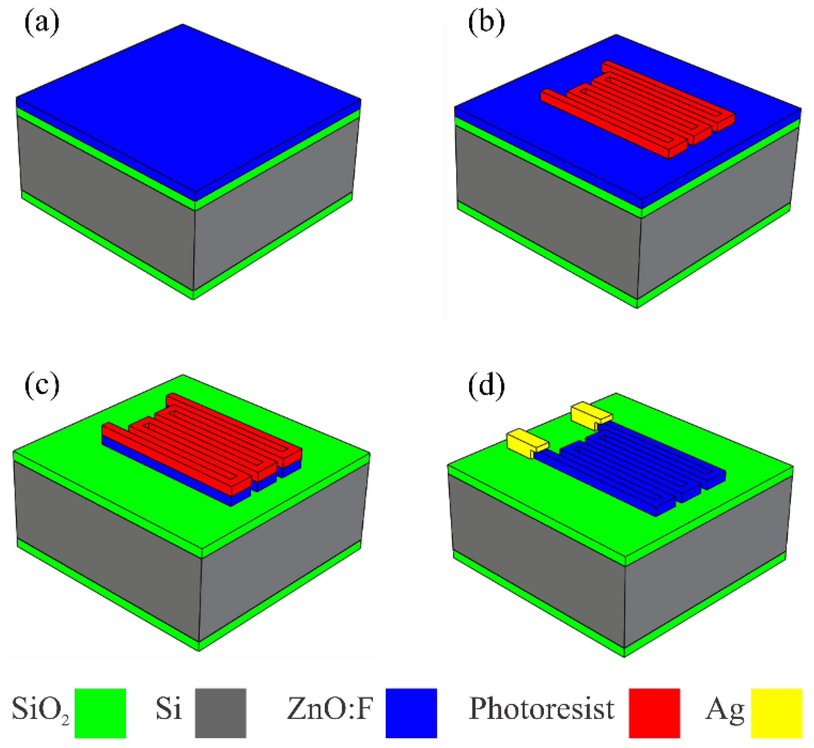
2.2. Characterization of Thin Films and Fabrication of the Cantilever Device

The electrical resistivity and thickness of the films were obtained using the four-point technique with a Keithley model 2400 sourceMeter and a Veeco Dektak 150 profilometer, respectively. The structural properties were determined using a Bruker model D8 ADVANCE diffractometer with Cu Kα radiation (λ = 1.5418 Å) (40 kV-40 mA).
The fabrication of the device starts from a rectangular Si (100) substrate with a 1 µm thick SiO2 layer on its surface for electrical insulation. To obtain the ZnO: F piezoresistor, lithography and chemical etching techniques were used, followed by the placement of contacts with conductive silver paste (Sigma Aldrich 735825–25G, resistivity 10−5 Ω.cm), as shown in Figure 1. The design of the ZnO: F piezoresistor and the dimensions of the substrate are shown in Figure 2.
The characterization of the change in the resistance of the ZnO: F piezoresistor caused by strain was carried out using a Keithley model 2400 source-Meter with a precision of 6.5 digits, and the cantilever method. The test consisted of fixing one end of the rectangular silicon substrate, where the piezoresistor is located next to it, while different masses were placed on the free end to cause deflection in the cantilever structure (see Figure 3).
The maximum strain in the cantilever structure occurred at the fixed end where the piezoresistor was located and was determined in two ways. For the first method, the following equation was used [30,31,32]:
ε = 6 Fl Ewt 2
where F is the load force caused by a mass (m) applied at the free end and the gravitational acceleration is F = mg [33]. For the case in which the thickness of the thin film is much thinner than the thickness of the support material, the strain (ε) is only a function of the length (l), width (w), thickness (t), and Young’s modulus (E) of the cantilever material [34,35].
The second method for obtaining the strain in the ZnO: F piezoresistor involved using a simulation in the COMSOL Multiphysics 5.3a FEM (finite element method) software. The dimensions and materials used were similar to those of the fabricated cantilever. The solid mechanics’ conditions included placing a fixed restraint at one end of the rectangular plate and applying different load forces at the free end (where the simulated load forces were the same applied to the fabricated cantilever). Physical properties such as density (kg/m3), Young’s modulus (GPa), and Poisson’s ratio used for the FEM simulation were 2330, 160, and 0.22 for silicon; 2200, 70, and 0.17 for SiO2; and 5676, 139, and 0.33 for ZnO: F, respectively. The Young’s modulus of ZnO: F is an average of the values reported for polycrystalline ZnO thin films with the hexagonal wurtzite phase [36,37,38,39]. All other parameter values were obtained from the COMSOL Multiphysics Materials Library and the literature published in [40,41,42].

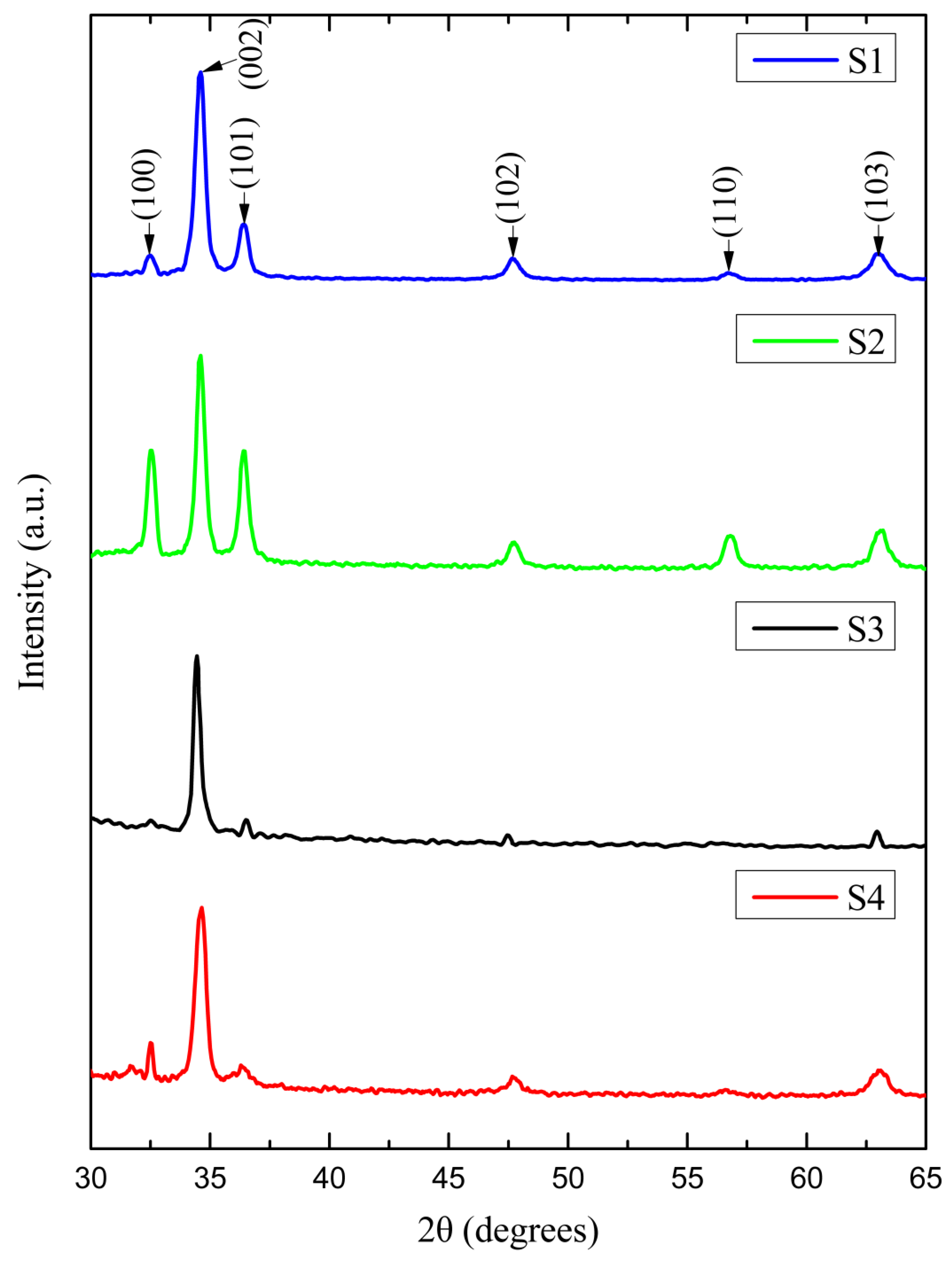
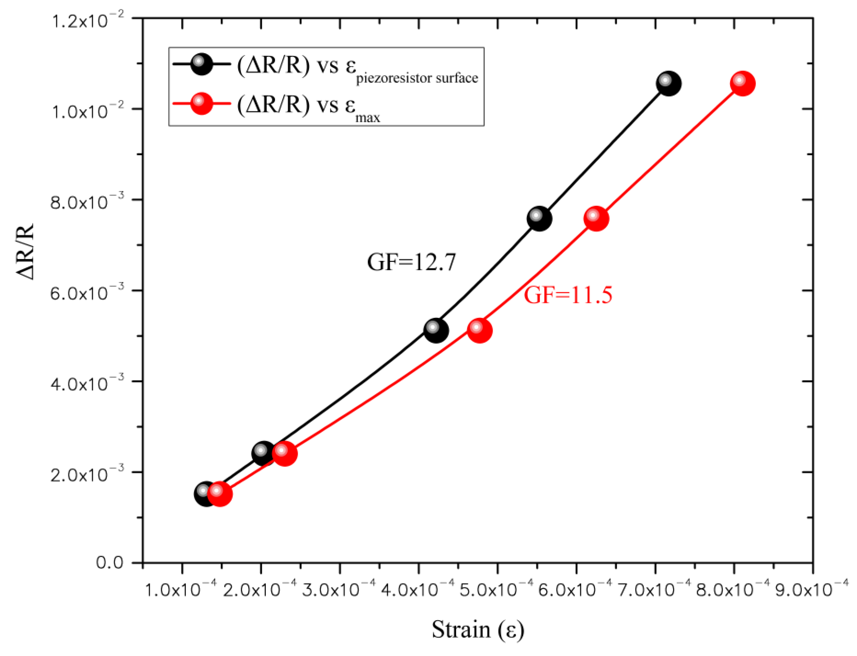
3. Results and Discussion

ZnO: F films were deposited on 25.4 × 25.4 mm borosilicate glass coverslips (S1 and S2) and quarters of a 50.8 mm diameter SiO2/Si wafer (S3 and S4). Thickness, resistivity, and sheet resistance were measured using profilometry and a four-point probe and are shown in Table 1. Due to the limitation of the deposit method to obtain regular thicknesses, variations between 234 and 295 nm were presented, with the result that the values of sheet resistance (Rsheet) and resistivity (ρ) which are related to thickness (d = ρ/Rsheet) also presented changes [43]; however, for small areas, this difference in thickness tends to decrease. On the other hand, the resistivities presented in the samples were around the order of 10−2 Ω.cm, which is in agreement with the values reported in the literature that range between 10−1 and 10−3 Ω.cm [44,45,46]. The lowest value obtained was 5.21 × 10⁻² Ω.cm for sample 1 deposited on a borosilicate glass coverslip substrate. The decrease in the resistivity of ZnO thin films is mainly attributed to the incorporation of F atoms at the O sites in the ZnO lattice, which in turn increases the carrier concentration [46,47,48].
Figure 4 shows the X-ray diffraction spectra of ZnO: F thin films (S1, S2, S3, and S4). All samples are polycrystalline where the positions of the peaks indicate a ZnO hexagonal wurtzite structure. No additional peaks corresponding to fluorine compounds were found, indicating that the fluorine dopant concentration is below the solubility limit [44,45,49,50,51].
On the other hand, the lattice parameters (a) and (c) for fluorine-doped ZnO thin films were estimated using the following equation [52]:
1 d h k l 2 = 4 3 ( h 2 + h k + k 2 ) a 2 + l 2 c 2
where dhkl is the interplanar spacing of the given Miller indices h, k, and l.
The results, given in Table 2, show minimum average decreases of 0.067% for the parameter (c) and 0.661% for (a), with respect to the standard values (a = 3.249 Å; c = 5.206 Å) for a film of hexagonal wurtzite ZnO taken from card 36-1451 of the Joint Committee on Powder Diffraction Standards (JCPDS). According to Vegard’s law [53,54], this decrease in the lattice parameters is indicative of a tiny narrowing of the ZnO lattice because the radius of the F−1 ions that replace the O−2 ions is slightly smaller in size (F−1 1.31 Å; O−2 1.38 Å) [55,56].
In addition to this, the preferential orientation of the ZnO: F films was obtained from the texture coefficients (TC) (hkl) defined as [56]:
TC ( h k l ) = I ( h k l ) / I 0 ( h k l ) ( 1 / n ) n I ( h k l ) / I 0 ( h k l )
where I(hkl) is the measured relative intensity of a plane (h k l), I0(hkl) is the standard intensity of the plane (hkl) taken from JCPDS data (card No. 36-1451), and n is the number of peaks of diffraction considered in the calculation.
The results of the calculated texture coefficients for the (100), (002), (101) planes (see Table 2) revealed that the preferential orientation along the (002) direction in all films with a c-axis predisposition of crystallites is perpendicular to the substrate surface [47,55,57].
Based on these results, sample 3 obtained adequate resistivity and crystallinity, and was therefore selected for the determination of strain and piezoresistive behavior via the cantilever method (see design and dimensions in Figure 2).
Below, Figure 5 shows the strain caused by the application of forces at the free end of the cantilever obtained using Equation (2) and finite element analysis (FEA) in COMSOL Multiphysics 5.3a. For the calculation of the theoretical strain, only the mechanical properties of the silicon cantilever structure were considered. In the case of the simulation, it was determined using the mechanical properties of Si, SiO2, and ZnO. The simulation results indicated that the maximum strain in the ZnO: F piezoresistor was almost equal to that of the Si substrate, showing a percentage error below 0.41% concerning the theoretically calculated value, which is attributed to the fact that the thickness of the film of ZnO: F (247 nm) was much smaller than that of the Si substrate (280 µm). This is in agreement with those reported in [34,35,58,59].
Figure 6 shows the change in resistance as a function of strain ε, where the variation in electrical resistance increases with the applied strain. According to Equation (1) and the experimental data obtained, the gauge factor calculated with the average strain on the piezoresistor surface was 12.7, and considering the maximum strain, the value was 11.5. On the other hand, for a polycrystalline material such as ZnO: F, the longitudinal piezoresistive coefficient (πl) can be expressed in terms of the gauge factor:
π l = GF E ZnO
where πl and EZnO represent the average value of all possible crystal directions and the Young’s modulus of polycrystalline ZnO, respectively [11,28]. Considering an average value of the Young’s modulus for polycrystalline ZnO thin films with the hexagonal wurtzite phase of 139 GPa [36,37,38,39], the longitudinal piezoresistive coefficient of ZnO: F for the gauge factor obtained with the average strain on the surface is approximately 9.13 × 10⁻¹¹ Pa−1.
Below, Table 3 summarizes the parameters and results of work reported on ZnO piezoresistive thin films and those of our proposed work. According to the work reported by Cardoso et al. [19] and Tuyaerts et al. [29], the piezoresistive effect of polycrystalline ZnO thin films is related to the intensity of the preferential orientation (002), where the c-axis of the wurtzite structure is perpendicular to the substrate surface. In addition to this, Cardoso et al. [15] observed that increasing the Al doping of ZnO films shifted the (002) preferential orientation to higher 2θ positions, causing a decrease in piezoresistive sensitivity as well as changes in the crystal lattice. On the other hand, de Luka et al. [28] associated the crystalline planes (0002) and (10-10) with the piezoresistivity of polycrystalline AZO films with different organic contents (0 to 4 vol%), indicating that the crystallites presented two possible orientations for the c-axis, with some being perpendicular to the plane and others being parallel to it. Another study developed by Ferreira et al. [27] reported the piezoresistive effect on Ag-doped ZnO nanostructured films, which developed a mixture of hexagonal (002) and (101) ZnO with a dominant fcc-Ag (111) phase.
Based on the literature and the results obtained (see Table 3), it can be seen that the deposition technique, temperature, type and level of doping, as well as the structural organization of the substrate used, are determining factors that notoriously modify the preferential orientation, which in turn influences the direction of stress in the crystallites, improving the piezoresistive sensitivity of ZnO thin films.
Subsequently, Figure 7 shows the characterization of the temperature coefficient of resistance (TCR) of the ZnO: F piezoresistor. Measurements were made using the four-point method from room temperature to 625 K. The results revealed a slow decrease in resistance as the temperature increases, observing an approximately constant negative TCR of −3.78 × 10⁻³ %/K up to 525 K (251.85 °C), after which the value of the resistance rises abruptly with the temperature and finally decreases again, coinciding with the results reported by Cardoso et al. [19]. According to Sahay et al. [60], this drastic increase in resistance is related to the adhesion of oxygen atoms to the film surface. Moreover, the subsequent decrease can be associated with the dominant thermal excitation of electrons and the release of oxygen atoms of the surface.

4. Conclusions

The gauge factor of a ZnO: F thin film, deposited with a homemade ultrasonic spray pyrolysis system, was evaluated using the cantilever method. The gauge factor of the ZnO: F film was 12.7, which is lower than that of Si and other semiconductors with values up to 200 but higher than that of metals (2–3). As for the TCR of the ZnO: F film, it was shown to be approximately stable up to 525 K (251.85 °C); it can therefore be another alternative added to SiC, diamond, and polysilicon to replace silicon, which is not suitable above 125 °C (398.15 K) due to the presence of current leakage.
We consider that ZnO: F films present interesting characteristics, such as a naturally well-defined crystallographic structure (wurtzite with (002) preferential orientation), adequate thermal stability, wide bandgap, transparency (unlike metals), and compatibility with microfabrication techniques, which could contribute positively to the development of future MEMS and NEMS sensors for the detection of pressure, force, acceleration, and vibration.

Author Contributions

Conceptualization, H.E.P.R. and S.A.I.; data curation, H.E.P.R., S.A.I. and B.S.S.C.; formal analysis, H.E.P.R., S.A.I. and B.S.S.C.; investigation, H.E.P.R., S.A.I., B.S.S.C. and J.I.M.S.; methodology, H.E.P.R. and S.A.I.; project administration, S.A.I. and B.S.S.C.; resources, S.A.I. and B.S.S.C.; supervision, S.A.I. and B.S.S.C.; validation, S.A.I. and B.S.S.C.; writing—original draft, H.E.P.R.; writing—review and editing, H.E.P.R., S.A.I., B.S.S.C. and J.I.M.S. All authors have read and agreed to the published version of the manuscript.

Funding

Hector Eduardo Petlacalco acknowledges the financial support of a CONACYT doctoral scholarship: 666452 from the Institute of Semiconductor Devices program at CIDS BUAP, as well as VIEP-BUAP for financial support with the publication fee.

Data Availability Statement

The data presented in this study are available from the corresponding author upon request.

Acknowledgments

Special thanks are due to Maribel García Miranda for the support provided in the field of chemistry and training in the semiconductor laboratory of the Eco campus BUAP Valsequillo.

Conflicts of Interest

All authors declare that they have no conflict of interest.

References

  1. Li, Y.; Wang, W.; Liao, K.; Hu, C.; Huang, Z.; Feng, Q. Piezoresistive effect in carbon nanotube films. Chin. Sci. Bull. 2003, 48, 125–127. [Google Scholar] [CrossRef]
  2. Fraga, M.A.; Furlan, H.; Pessoa, R.S.; Massi, M. Wide bandgap semiconductor thin films for piezoelectric and piezoresistive MEMS sensors applied at high temperatures: An overview. Microsyst. Technol. 2014, 20, 9–21. [Google Scholar] [CrossRef]
  3. Li, F.; Shen, T.; Wang, C.; Zhang, Y.; Qi, J.; Zhang, H. Recent Advances in Strain-Induced Piezoelectric and Piezoresistive Effect-Engineered 2D Semiconductors for Adaptive Electronics and Optoelectronics. Nano-Micro Lett. 2020, 12, 106. [Google Scholar] [CrossRef]
  4. Kumar, S.S.; Pant, B.D. Design principles and considerations for the “ideal” silicon piezoresistive pressure sensor: A focused review. Microsyst. Technol. 2014, 20, 1213–1247. [Google Scholar] [CrossRef]
  5. Li, C.; Cordovilla, F.; Jagdheesh, R.; Ocaña, J.L. Design Optimization and Fabrication of a Novel Structural SOI Piezoresistive Pressure Sensor with High Accuracy. Sensors 2018, 18, 439. [Google Scholar] [CrossRef] [Green Version]
  6. Li, X.; Liu, Q.; Pang, S.; Xu, K.; Tang, H.; Sun, C. High-temperature piezoresistive pressure sensor based on implantation of oxygen into silicon wafer. Sens. Actuators A Phys. 2012, 179, 277–282. [Google Scholar] [CrossRef]
  7. Sheeparamatti, B.G.; Balavalad, K.B. Fabrication and characterization of polysilicon-on-insulator (PolySOI) and a-SOI based micro piezoresistive pressure sensor for harsh environment applications. Microsyst. Technol. 2019, 25, 4119–4133. [Google Scholar] [CrossRef]
  8. Guo, S.; Eriksen, H.; Childress, K.; Fink, A.; Hoffman, M. High temperature high accuracy piezoresistive pressure sensor based on smart-cut soi. In Proceedings of the 2008 IEEE 21st International Conference on Micro Electro Mechanical Systems, Tucson, AZ, USA, 13–17 January 2008. [Google Scholar]
  9. Doll, J.C.; Pruitt, B.L. Alternative Materials and Transduction Methods. In Piezoresistor Design and Applications. Microsystems and Nanosystems; Springer: New York, NY, USA, 2013; Volume 1. [Google Scholar]
  10. Fiorillo, A.S.; Critello, C.D.; Pullano, A.S. Theory, Technology and Applications of Piezoresistive Sensors: A Review. Sens. Actuator A Phys. 2018, 281, 156–175. [Google Scholar] [CrossRef]
  11. Werner, M.; Gluche, P.; Adamschik, M.; Kohn, E.; Fecht, H.-J. Review on diamond based piezoresistive sensors. In Proceedings of the IEEE International Symposium on Industrial Electronics, Pretoria, South Africa, 7–10 July 1998. [Google Scholar]
  12. Li, C.; Cordovilla, F.; Ocaña, J.L. The design and analysis of a novel structural piezoresistive pressure sensor for low pressure measurement. Microsyst. Technol. 2017, 23, 5677–5687. [Google Scholar] [CrossRef]
  13. Azhari, F.; Banthia, N. Cement-based sensors with carbon fibers and carbon nanotubes for piezoresistive sensing. Cem. Concr. Compos. 2012, 34, 866–873. [Google Scholar] [CrossRef]
  14. French, P.J.; Evans, A.G.R. Piezoresistance in polysilicon and its applications to strain gauges. Solid-State Electron. 1989, 32, 1–10. [Google Scholar] [CrossRef]
  15. Cardoso, G.W.A.; Leal, G.; Massi, M.; da Silva Sobrinho, A.S.; Libardi, J. The influence of aluminum incorporation on the structural and electrical properties of ZnO thin films for applications in piezoresistive sensors. In Proceedings of the 2017 32nd Symposium on Microelectronics Technology and Devices (SBMicro), Fortaleza, Brazil, 28 August–1 September 2017. [Google Scholar]
  16. Samoei, V.K.; Jayatissa, A.H. Aluminum doped zinc oxide (AZO)-based pressure sensor. Sens. Actuators A Phys. 2020, 303, 111816. [Google Scholar] [CrossRef]
  17. Zeng, Q.; Lei, D.; Zhang, Y.; Huang, H. Transferable self-supporting ZnO porous films for low-cost piezoresistive sensors. Semicond. Sci. Technol. 2014, 29, 045009. [Google Scholar] [CrossRef]
  18. Inomata, N.; Van Toan, N.; Ono, T. Piezoresistive property of an aluminum-doped zinc oxide thin film deposited via atomic-layer deposition for microelectromechanical system/nanoelectromenchanical system applications. IEEE J. Trans. Electr. Electron. Eng. 2017, 12, 120–124. [Google Scholar] [CrossRef]
  19. Cardoso, G.W.A.; Leal, G.; da Silva Sobrinho, A.S.; Fraga, M.A.; Massi, M. Evaluation of piezoresistivity properties of sputtered ZnO thin films. Mater. Res. 2014, 17, 588–592. [Google Scholar] [CrossRef] [Green Version]
  20. Gregory, O.J.; Slot, A.B.; Amons, P.S.; Crisman, E.E. High temperature strain gages based on reactively sputtered AlNx thin films. Surf. Coat. Technol. 1997, 88, 79–89. [Google Scholar] [CrossRef]
  21. Yan, W.; Fuh, H.R.; Lv, Y.; Chen, K.Q.; Tsai, T.Y.; Wu, Y.R.; Shieh, T.H.; Hung, K.M.; Li, J.; Zhang, D.; et al. Giant gauge factor of Van der Waals material based strain sensors. Nat. Commun. 2021, 12, 2018. [Google Scholar] [CrossRef]
  22. Erskine, J.C. Polycrystalline silicon-on-metal strain gauge transducers. IEEE Trans. Electron. Dev. 1983, 30, 796–801. [Google Scholar] [CrossRef]
  23. Onuma, Y.; Kamimura, K.; Homma, Y. Piezoresistive elements of polycrystalline semiconductor thin films. Sens. Actuators 1988, 13, 71–77. [Google Scholar] [CrossRef]
  24. Obieta, I.; Gracia, F.J. Sputtered silicon thin films for piezoresistive pressure microsensors. Sens. Actuators A Phys. 1994, 42, 685–688. [Google Scholar] [CrossRef]
  25. Fraga, M.A.; Furlan, H.; Pessoa, R.S.; Rasia, L.A.; Mateus, C.F.R. Studies on SiC, DLC and TiO2 thin films as piezoresistive sensor materials for high temperature application. Microsyst. Technol. 2012, 18, 1027–1033. [Google Scholar] [CrossRef]
  26. Phan, H.-P.; Viet Dao, D.; Tanner, P.; Wang, L.; Nguyen, N.-T.; Zhu, Y.; Dimitrijev, S. Fundamental piezoresistive coefficients of p-type single crystalline 3C-SiC. Appl. Phys. Lett. 2014, 104, 111905. [Google Scholar] [CrossRef]
  27. Ferreira, A.; Silva, J.P.; Rodrigues, R.; Martin, N.; Lanceros-Méndez, S.; Vaz, F. High performance piezoresistive response of nanostructured ZnO/Ag thin films for pressure sensing applications. Thin Solid Film. 2019, 691, 137587. [Google Scholar] [CrossRef]
  28. Luka, G.; Wachnicki, L.; Witkowski, B.S.; Jakiela, R.; Virt, I.S. Structure-property relationships in ZnO:Al-hydroquinone films grown on flexible substrates by atomic and molecular layer deposition. Mater. Des. 2017, 119, 297–302. [Google Scholar] [CrossRef]
  29. Tuyaerts, R.; Poncelet, O.; Raskin, J.-P.; Proost, J. Internal stress and opto-electronic properties of ZnO thin films deposited by reactive sputtering in various oxygen partial pressures. J. Appl. Phys. 2017, 122, 155306. [Google Scholar] [CrossRef]
  30. Lakhmi, R.; Debeda, H.; Dufour, I.; Lucat, C. Force Sensors Based on Screen-Printed Cantilevers. IEEE Sens. J. 2010, 10, 1133–1137. [Google Scholar] [CrossRef] [Green Version]
  31. Pérez, R.; Chaillet, N.; Domanski, K.; Janus, P.; Grabiec, P. Fabrication, modeling and integration of a silicon technology force sensor in a piezoelectric micro-manipulator. Sens. Actuators A Phys. 2006, 128, 367–375. [Google Scholar] [CrossRef] [Green Version]
  32. Lee, C.; Thillaigovindan, J.; Chen, C.-C.; Chen, X.T.; Chao, Y.-T.; Tao, S.; Xiang, W.; Yu, A.; Feng, H.; Lo, G.Q. Si nanophotonics based cantilever sensor. Appl. Phys. Lett. 2008, 93, 113113. [Google Scholar] [CrossRef]
  33. Bao, M.-H. Micro Mechanical Transducers: Pressure Sensors, Accelerometers and Gyroscopes, 1st ed.; Elsevier Science: Amsterdam, The Netherlands, 2000. [Google Scholar]
  34. Hindrichsen, C.G.; Lou-Møller, R.; Hansen, K.; Thomsen, E.V. Advantages of PZT thick film for MEMS sensors. Sens. Actuators A Phys. 2010, 163, 9–14. [Google Scholar] [CrossRef]
  35. Liu, C. Foundations of MEMS, 2nd ed.; Pearson Education: Upper Saddle River, NJ, USA, 2006. [Google Scholar]
  36. Cheng, Y.; Liao, Y.; Li, J.; Guo, Z.-S. Mechanical characterization of zinc oxide thin films on glass substrates by nanoindentation. In Proceedings of the Second International Conference on Smart Materials and Nanotechnology in Engineering, Weihai, China, 20 October 2009. [Google Scholar]
  37. Fang, T.-H.; Chang, W.-J.; Lin, C.-M. Nanoindentation characterization of ZnO thin films. Mater. Sci. Eng. A 2007, 452–453, 715–720. [Google Scholar] [CrossRef]
  38. Tapily, K.; Gu, D.; Baumgart, H.; Namkoong, G.; Stegall, D.; Elmustafa, A.A. Mechanical and structural characterization of atomic layer deposition-based ZnO films. Semicond. Sci. Technol. 2011, 26, 115005. [Google Scholar] [CrossRef]
  39. Tuyaerts, R.; Raskin, J.-P.; Proost, J. Electromechanical testing of ZnO thin films under high uniaxial strain. In Proceedings of the 2017 International Conference of Microelectronic Test Structures (ICMTS), Grenoble, France, 28–30 March 2017. [Google Scholar]
  40. Farhath, M.; Samad, M.F. Design and simulation of a high sensitive stripped-shaped piezoresistive pressure sensor. J. Comput. Electron. 2020, 19, 310–320. [Google Scholar] [CrossRef]
  41. Senturia, S.D. Microsystem Design; Springer: Boston MA, USA, 2002. [Google Scholar]
  42. Bannikoppa, S.; Katageri, A.C.; Balavalad, K.B.; Sheeparamatti, B.G. Design of piezoresistive pressure sensor for enhanced sensitivity. In Proceedings of the 2016 International Conference on Energy Efficient Technologies for Sustainability, Nagercoil, India, 7–8 April 2016. [Google Scholar]
  43. Rao, P.T.; Santhoshkumar, M.C. Highly oriented (100) ZnO thin films by spray pyrolysis. Appl. Surf. Sci. 2009, 255, 7212–7215. [Google Scholar]
  44. Guillén-Santiago, A.; Olvera, M.d.l.L.; Maldonado, A.; Asomoza, R.; Acosta, D.R. Electrical, structural and morphological properties of chemically sprayed F-doped ZnO films: Effect of the ageing-time of the starting solution, solvent and substrate temperature. Phys. Stat. Sol. A 2004, 201, 952–959. [Google Scholar] [CrossRef]
  45. Rodríguez-Báez, J.; Maldonado, A.; Castañeda, L.; Delgado, G.T.; Castanedo-Pérez, R.; Olvera, M.d.l.L. On the effect of acetic acid on physical properties of chemically sprayed fluorine-doped ZnO thin films. Thin Solid Film. 2007, 515, 8689–8694. [Google Scholar] [CrossRef]
  46. Anandhi, R.; Mohan, R.; Swaminathan, K.; Ravichandran, K. Influence of aging time of the starting solution on the physical properties of fluorine doped zinc oxide films deposited by a simplified spray pyrolysis technique. Superlattices Microstruct. 2012, 51, 680–689. [Google Scholar] [CrossRef]
  47. Rodríguez-Báez, J.; Maldonado, A.; Torres-Delgado, G.; Castanedo-Pérez, R.; Olvera, M.d.l.L. Influence of the molar concentration and substrate temperature on fluorine-doped zinc oxide thin films chemically sprayed. Mater. Lett. 2006, 60, 1594–1598. [Google Scholar] [CrossRef]
  48. Biswal, R.R.; Velumani, S.; Babu, B.J.; Maldonado, A.; Tirado-Guerra, S.; Castañeda, L.; Olvera, M.d.l.L. Fluorine doped zinc oxide thin films deposited by chemical spray, starting from zinc pentanedionate and hydrofluoric acid: Effect of the aging time of the solution. Mater. Sci. Eng. B 2010, 174, 46–49. [Google Scholar] [CrossRef]
  49. Pawar, B.N.; Ham, D.-H.; Mane, R.S.; Ganesh, T.; Cho, B.-W.; Han, S.-H. Fluorine-doped zinc oxide transparent and conducting electrode by chemical spray synthesis. Appl. Surf. Sci. 2008, 254, 6294–6297. [Google Scholar] [CrossRef]
  50. Gunasekaran, E.; Ezhilan, M.; Mani, G.K.; Shankar, P.; Kulandaisamy, A.J.; Rayappan, J.B.B.; Babu, K.J. Fluorine doped ZnO thin film as acetaldehyde sensor. Semicond. Sci. Technol. 2018, 33, 095005. [Google Scholar] [CrossRef]
  51. Shinde, S.S.; Shinde, P.S.; Pawar, S.M.; Moholkar, A.V.; Bhosale, C.H.; Rajpure, K.Y. Physical properties of transparent and conducting sprayed fluorine doped zinc oxide thin films. Solid State Sci. 2008, 10, 1209–1214. [Google Scholar] [CrossRef]
  52. Alkhayatt, A.H.O.; Hussian, S.K. Fluorine dopant concentration effect on the structural and optical properties of spray deposited nanocrystalline ZnO thin films. Surf. Interfaces 2017, 8, 176–181. [Google Scholar] [CrossRef]
  53. Nakrela, A.; Benramdane, N.; Bouzidi, A.; Kebbab, Z.; Medles, M.; Mathieu, C. Site location of Al-dopant in ZnO lattice by exploiting the structural and optical characterisation of ZnO:Al thin films. Results Phys. 2016, 6, 133–138. [Google Scholar] [CrossRef] [Green Version]
  54. Pearson, G.L.; Bardeen, J. Electrical Properties of Pure Silicon and Silicon Alloys Containing Boron and Phosphorus. Phys. Rev. 1949, 75, 865–883. [Google Scholar] [CrossRef]
  55. Sanchez-Juarez, A.; Tiburcio-Silver, A.; Ortiz, A.; Zironi, E.P.; Rickards, J. Electrical and optical properties of fluorine-doped ZnO thin films prepared by spray pyrolysis. Thin Solid Film. 1998, 333, 196–202. [Google Scholar] [CrossRef]
  56. Douayar, A.; Diaz, R.; Cherkaoui El Moursli, F.; Schmerber, G.; Dinia, A.; Abd-Lefdil, M. Fluorine-doped ZnO thin films deposited by spray pyrolysis technique. Eur. Phys. J. Appl. Phys. 2011, 53. [Google Scholar] [CrossRef]
  57. Sanchez-Juarez, A.; Tiburcio-Silver, A.; Ortiz, A. Properties of fluorine-doped ZnO deposited onto glass by spray pyrolysis. Sol. Energy Mater. Sol. Cells 1998, 52, 301–311. [Google Scholar] [CrossRef]
  58. Phan, H.-P.; Dinh, T.; Kozeki, T.; Qamar, A.; Namazu, T.; Dimitrijev, S.; Nguyen, N.-T.; Dao, D.V. Piezoresistive effect in p-type 3C-SiC at high temperatures characterized using Joule heating. Sci. Rep. 2016, 6, 28499. [Google Scholar] [CrossRef] [Green Version]
  59. Dao, D.V.; Phan, H.-P.; Qamar, A.; Dinh, T. Piezoresistive effect of p-type single crystalline 3C–SiC on (111) plane. RSC Adv. 2016, 6, 21302–21307. [Google Scholar] [CrossRef] [Green Version]
  60. Sahay, P.P.; Nath, R.K. Al-doped ZnO thin films as methanol sensors. Sens. Actuators B Chem. 2008, 134, 654–659. [Google Scholar] [CrossRef]
Figure 1. Piezoresistor manufacturing process: (a) deposition of a ZnO: F thin film via ultrasonic spray pyrolysis; (b) photoresist deposition with spin coating and piezoresistor pattern formation with lithography; (c) chemical etching with H3PO4 + CH3COOH + H2O (1:1:50) for resistance formation; (d) placement of conductive Ag paste contacts (Sigma Aldrich 735825-25G, resistivity 10−5 Ω.cm).
Crystals 12 01607 g001
Figure 2. Cantilever device design with ZnO: F piezoresistor.
Crystals 12 01607 g002
Figure 3. (a) Photograph of the cantilever method implemented for the characterization of the ZnO: F thin-film piezoresistor (resistance change measurements under deformation conditions of the piezoresistor were performed at room temperature and isolated from light); (b) schematic drawing of the circuit used for the measurement.
Crystals 12 01607 g003
Figure 4. X-ray diffraction spectra of ZnO: F thin films deposited via ultrasonic spray pyrolysis.
Crystals 12 01607 g004
Figure 5. (a) Results of the finite element analysis (FEM) of the piezoresistor strain caused by the application of forces at the free end of the cantilever; (b) average strain extracted via simulation of the ZnO: F patterned surface versus theoretically calculated strain.
Crystals 12 01607 g005
Figure 6. Relative change in resistance (∆R/R) as a function of strain ε.
Crystals 12 01607 g006
Figure 7. ZnO: F thin-film resistor temperature coefficient.
Crystals 12 01607 g007
Table 1. Profilometry and four-point probe.
SamplesThickness
(nm)
ρ × 10−2
(Ω.cm)
Rsheet × 103
(Ω)
S1295 ± 265.211.76
S2273 ± 2216.325.97
S3247 ± 277.382.98
S4234 ± 258.793.75
Table 2. Lattice parameters and texture coefficients of ZnO: F films.
Samplesa (Å)c (Å)TC (100)TC (002)TC (101)
S13.2335.2010.2272.4760.275
S23.2225.2000.7671.8930.439
S33.2335.2050.3142.5010.184
S43.2335.2010.4192.3030.177
Table 3. Parameters and results of the works reported on ZnO piezoresistive thin films.
Thin FilmStructureDeposit Method
and Temperature
GFπl
(Pa−1)
Bending
Method
SubstrateRef.
Al-doped ZnO
(AZO)
Polycrystalline:
hexagonal wurtzite
Preferential orientation: (002)
C-axis perpendicular to the surface
DC
magnetron
Co-sputtering
200 °C
Not
reported
Not
reported
Cantilever beamSiO2/Si[15]
ZnO
with
23 at. %
Ag
doping
A mixture between hexagonal
ZnO (002) and (101) with the
phase fcc-Ag (111)
Glancing
angle deposition (GLAD)
room
temperature
19
(Low strain)
122
(Medium strain)
Not
reported
System
(Shimadzu-AG-IS
universal testing
machine)
Biaxial-oriented PET[27]
ZnO
with
5% Al
doping
Not reportedAtomic layer deposition (ALD)
200 °C.
8.5Not
reported
Cantilever beamSiO2/Si[18]
AZO
with
1 vol %
organic
content
Polycrystalline with predominant
(10-10) plane and presence of the (0002) plane (indicating that some crystallites were oriented with the c-axis perpendicular to the plane and others had the c-axis parallel to the plane)
Atomic layer deposition (ALD)
140 °C
−9.5−6.6 × 10⁻¹¹Film
bending radius
Al2O3-coated PET[28]
ZnOPolycrystalline:
hexagonal wurtzite
Preferential orientation: (002)
C-axis perpendicular to the surface
RF reactive magnetron sputtering
annealed at 600 °C
2.6Not
reported
Cantilever beamSiO2/Si[19]
ZnOPolycrystalline:
hexagonal wurtzite
Preferential orientation: (002)
C-axis perpendicular to the surface
DC reactive
magnetron sputtering
−8.5Not reportedBent
substrate
SiO2[29]
ZnO
with
15 at. %
F doping
Polycrystalline:
hexagonal wurtzite
Preferential
orientation: (002)
C-axis perpendicular to the surface
Ultrasonic
spray pyrolysis (homemade
system)
450 °C
12.79.13 × 10−11Cantilever beamSiO2/SiOur work
Publisher’s Note: MDPI stays neutral with regard to jurisdictional claims in published maps and institutional affiliations.

