
Numerical Analysis and Experimental Verification of Resistance Additive Manufacturing

Abstract
:1. Introduction
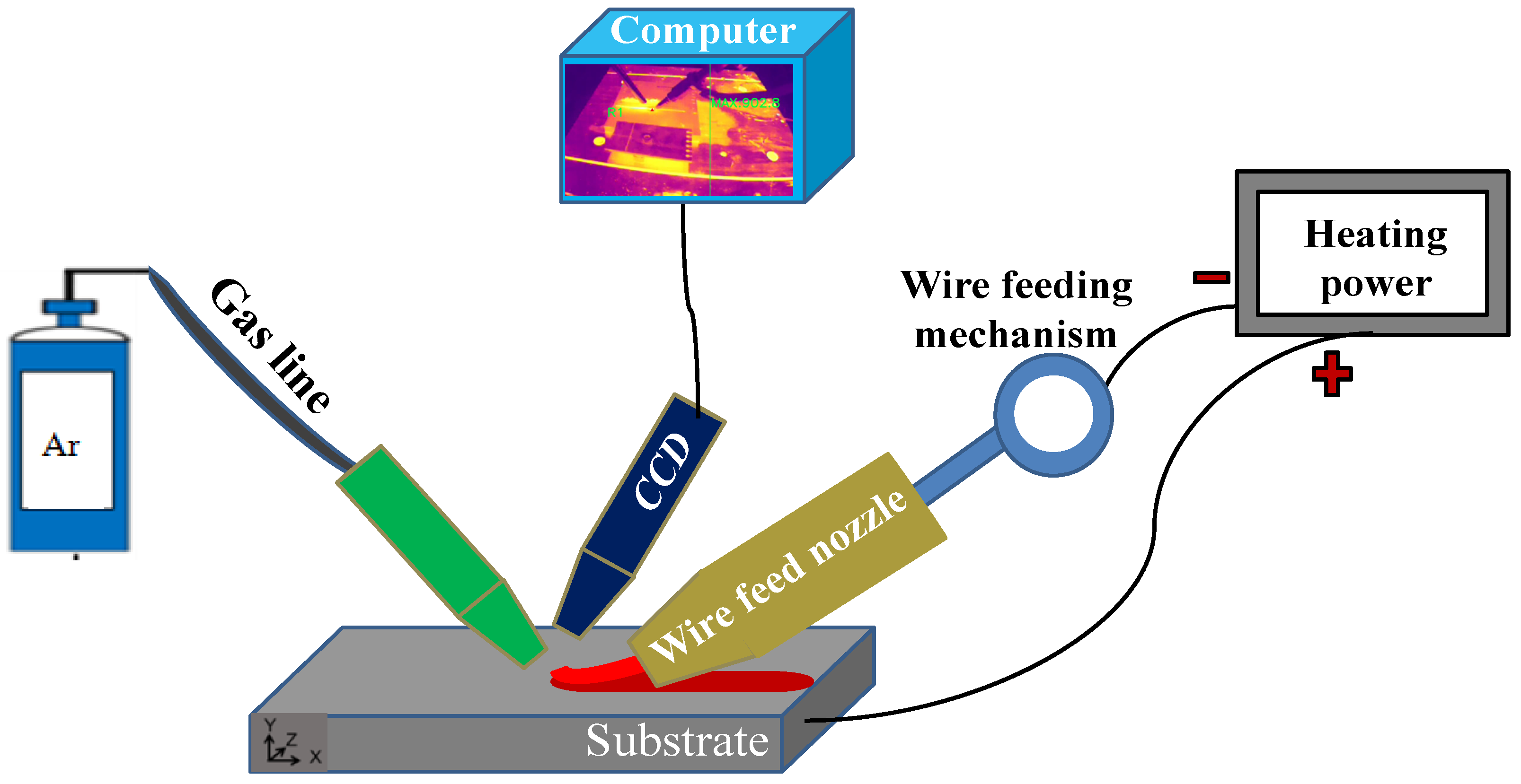
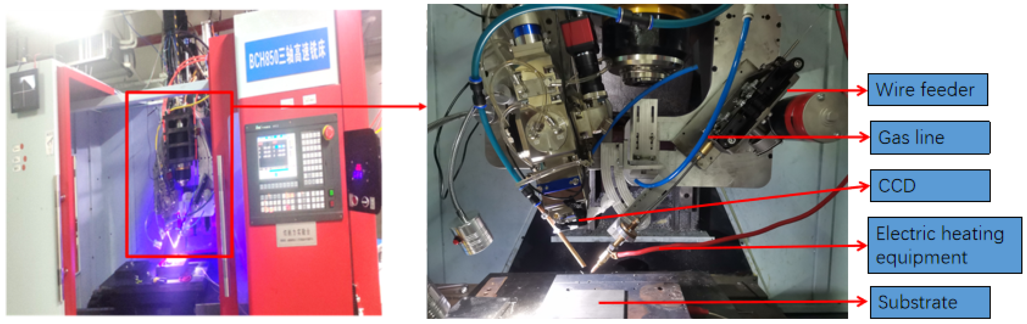
2. Materials and Methods
3. Numerical Simulation
3.1. Deposition Principle and Establishment of Temperature Field Equation
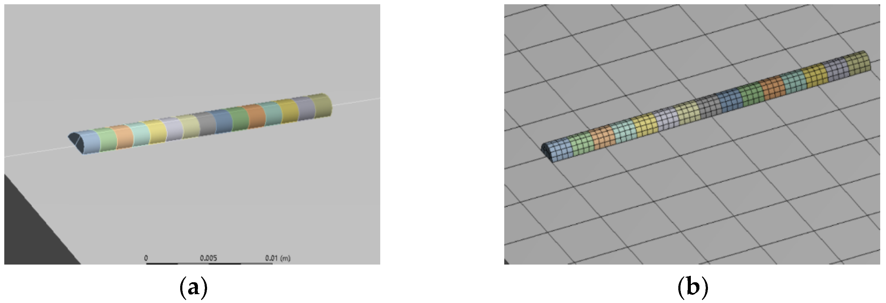
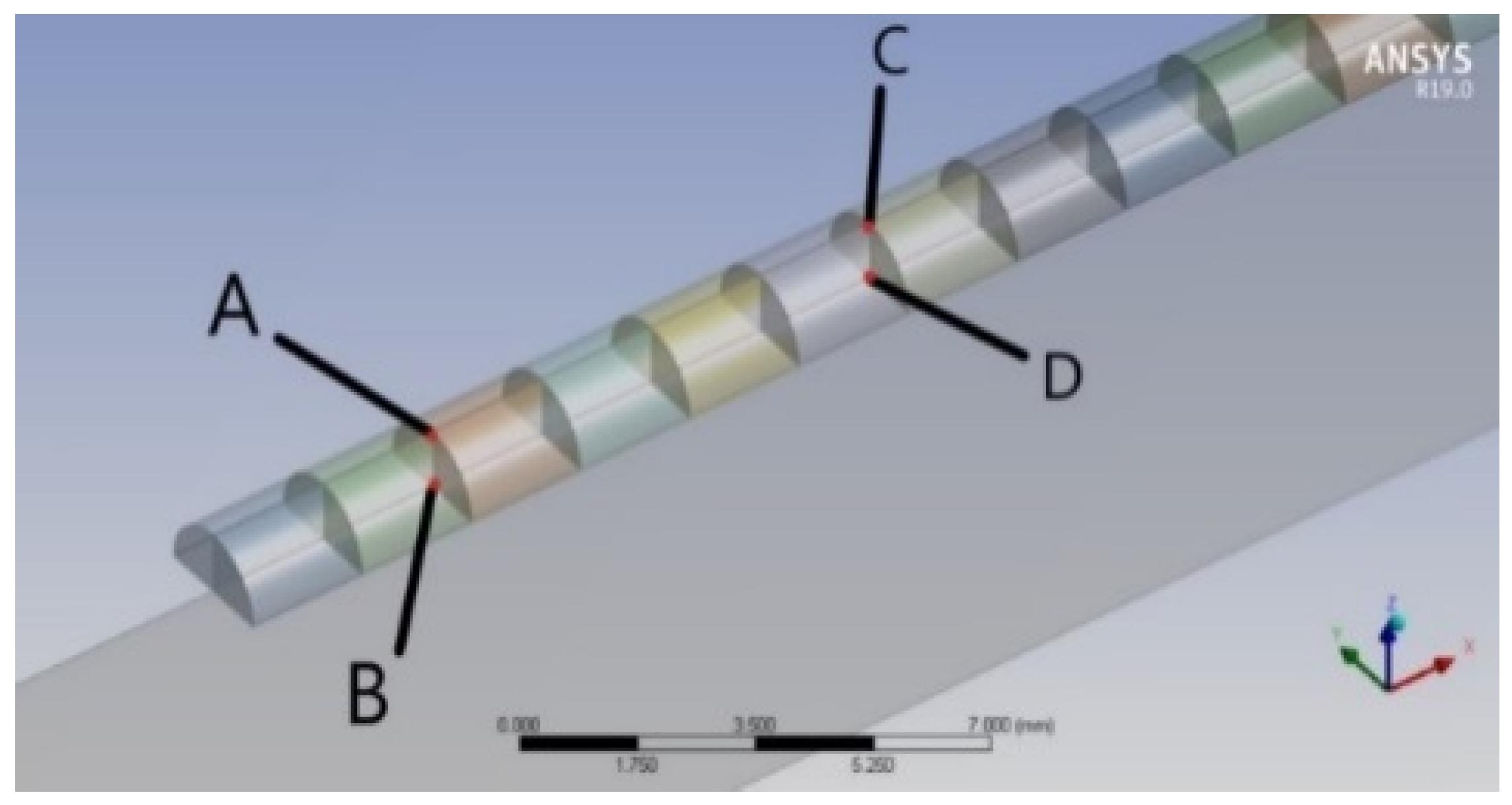
3.2. Geometric Model and Meshing
- (1)
- The heat transfer of materials in solid and molten states is continuous, and the parameters such as thermal conductivity and specific heat capacity involved in heat transfer are treated according to the continuous heat transfer.
- (2)
- The loaded resistance heat source is the body heat source, which is loaded in the form of command flow generated by the expression of heat flux at the classical Ansys interface in the transient thermal analysis.
- (3)
- It is assumed that the thermal absorption rate and thermal conductivity of the material do not change in the printing process.
- (4)
- The effect of latent heat on temperature field is ignored.
3.3. Material Assignment and Boundary Setting
3.3.1. Material Assignment
3.3.2. Boundary Conditions
3.3.3. Insertion of Life and Death Unit
3.3.4. Selection of Heat Sources and Application of Loads
3.4. Parameter Setting
4. Results
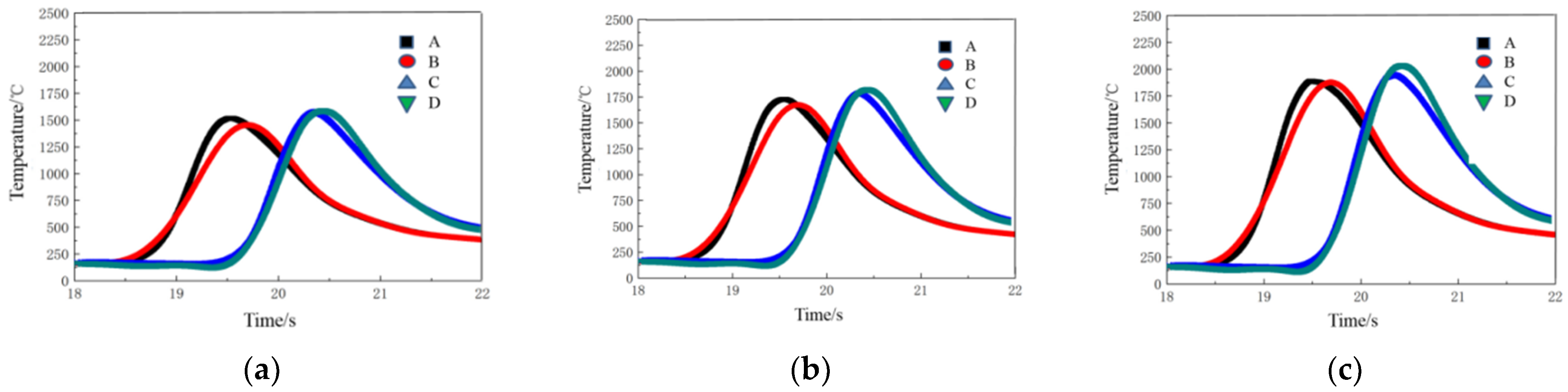
4.1. Results of Simulation
4.2. Influence of Current on Forming Appearance
4.3. Influence of Wire Feeding Speed on Forming Appearance
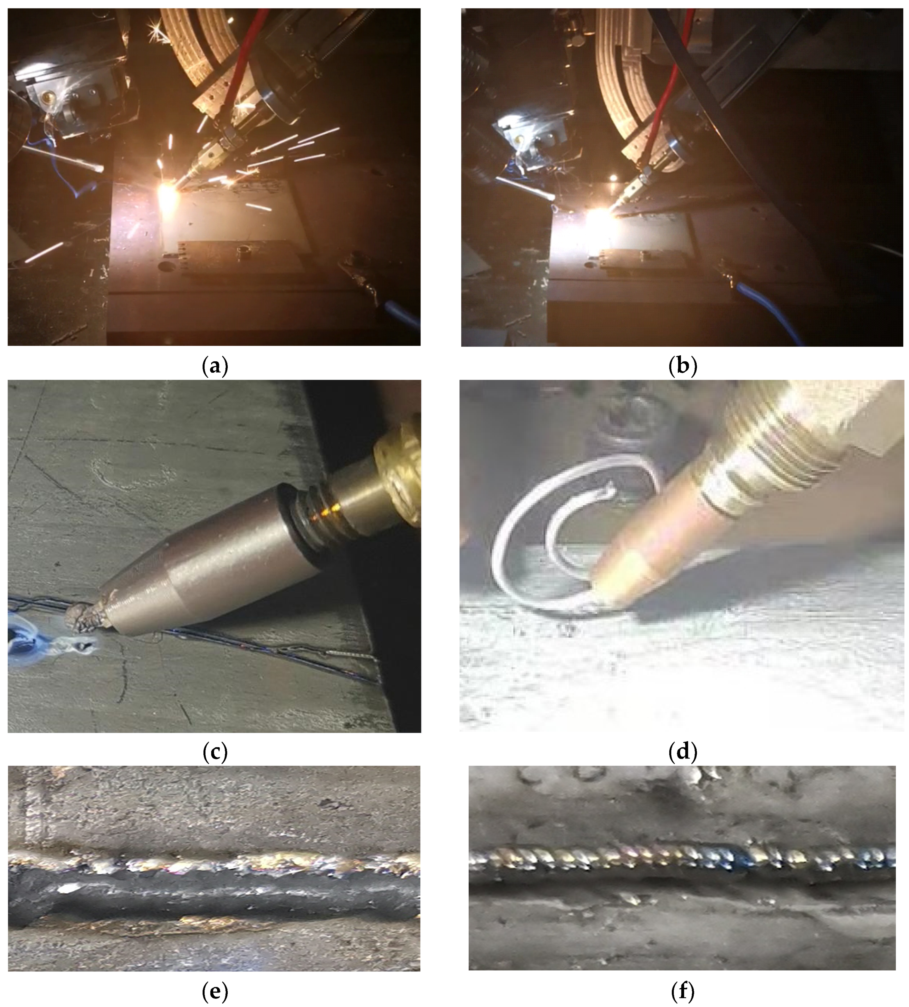
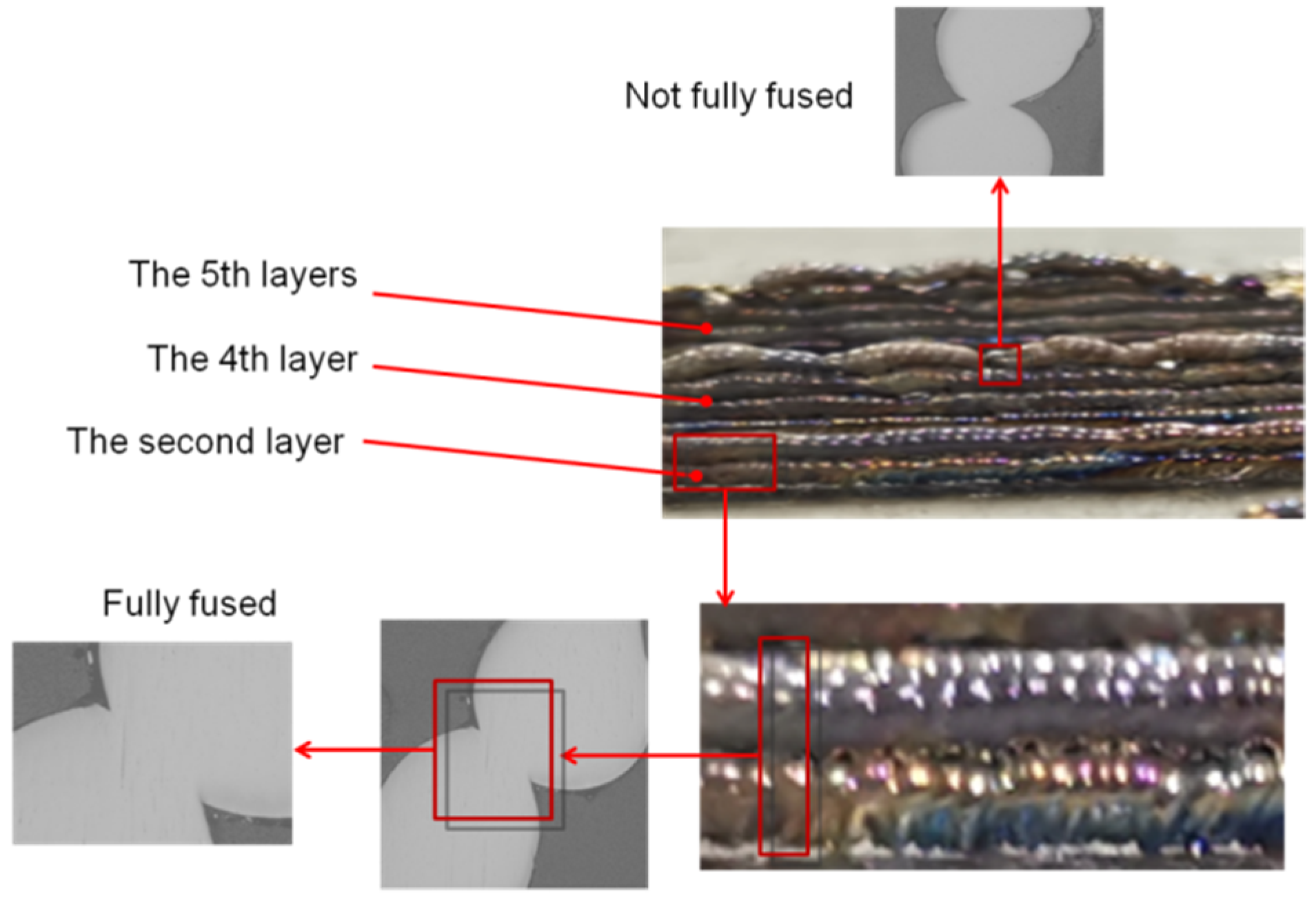
4.4. Forming and Density Test of Single-Pass Multilayer
5. Conclusions
- (1)
- In the RAM process, the main influencing factors are current, wire feeding speed, voltage, workbench moving speed, and gas flow. Current and wire feeding speed mainly affect the appearance of the molten coating layer. Voltage affects whether spark splash occurs in the printing process. Platform moving speed affects whether the printing process is at the correct temperature. Gas flow affects the oxidation degree.
- (2)
- When the material is Ti-6Al-4V, the current is 160 A, the voltage is 10 V, the wire feeding speed is 2.4 m/min, the moving speed of the workbench is 5 mm/s, and the gas flow rate is 0.7 m3/h, the forming morphology of the single-channel coating layer is the best.
- (3)
- By optimizing the process, a single-channel five-layer sample was printed, and its relative density was 97.7%. Good overlap between layers was achieved, which verified the feasibility of RAM at the experimental level and provided reference data for the subsequent development of this technology.
Author Contributions
Funding
Institutional Review Board Statement
Informed Consent Statement
Data Availability Statement
Acknowledgments
Conflicts of Interest
References
- Lu, B. Additive manufacturing—Current situation and future. China Mech. Eng. 2020, 31, 19. [Google Scholar]
- Calignano, F. Additive Manufacturing (AM) of Metallic Alloys. Crystals 2020, 10, 704. [Google Scholar] [CrossRef]
- Frazier, W.E. Metal additive manufacturing: A review. J. Mater. Eng. Perform. 2014, 23, 1917–1928. [Google Scholar] [CrossRef]
- Sun, C.; Wang, Y.; McMurtrey, M.D.; Jerred, N.D.; Liou, F.; Li, J. Additive manufacturing for energy: A review. Appl. Energy 2021, 282, 116041. [Google Scholar] [CrossRef]
- Jackson, M.A.; Van Asten, A.; Morrow, J.D.; Min, S.; Pfefferkorn, F.E. A comparison of energy consumption in wire-based and powder-based additive-subtractive manufacturing. Procedia Manuf. 2016, 5, 989–1005. [Google Scholar] [CrossRef] [Green Version]
- Węglowski, M.S.; Błacha, S.; Jachym, R.; Dworak, J.; Rykała, J. Additive manufacturing with wire–Comparison of processes. AIP Conf. Proc. 2019, 2113, 150016. [Google Scholar]
- Vimal, K.E.K.; Srinivas, M.N.; Rajak, S. Wire arc additive manufacturing of aluminium alloys: A review. Mater. Today Proc. 2021, 41, 1139–1145. [Google Scholar] [CrossRef]
- Hwang, M.J.; Cho, J. Laser Additive Manufacturing Technology Review. J. Weld. Join. 2014, 32, 354–357. [Google Scholar]
- Yilmaz, O.; Ugla, A.A. Shaped metal deposition technique in additive manufacturing: A review. Proc. Inst. Mech. Eng. Part B J. Eng. Manuf. 2016, 230, 1781–1798. [Google Scholar] [CrossRef]
- Galati, M.; Calignano, F.; Viccica, M.; Iuliano, L. Additive manufacturing redesigning of metallic parts for high precision machines. Crystals 2020, 10, 161. [Google Scholar] [CrossRef] [Green Version]
- Ding, Y.; Akbari, M.; Kovacevic, R. Process planning for laser wire-feed metal additive manufacturing system. Int. J. Adv. Manuf. Technol. 2018, 95, 355–365. [Google Scholar] [CrossRef]
- Fuchs, J.; Schneider, C.; Enzinger, N. Wire-based additive manufacturing using an electron beam as heat source. Weld. World 2018, 62, 267–275. [Google Scholar] [CrossRef] [Green Version]
- Miyata, Y.; Okugawa, M.; Koizumi, Y.; Nakano, T. Inverse columnar-equiaxed transition (CET) in 304 and 316 L stainless steels melt by electron beam for additive manufacturing (AM). Crystals 2021, 11, 856. [Google Scholar] [CrossRef]
- Węglowski, M.S.; Błacha, S.; Pilarczyk, J.; Dutkiewicz, J.; Rogal, Ł. Electron beam additive manufacturing with wire–analysis of the process. AIP Conf. Proc. 2018, 1960, 140015. [Google Scholar]
- Rodrigues, T.A.; Duarte, V.; Miranda, R.M.; Santos, T.G.; Oliveira, J.P. Current status and perspectives on wire and arc additive manufacturing (WAAM). Materials 2019, 12, 1121. [Google Scholar] [CrossRef] [Green Version]
- Derekar, K.S. A review of wire arc additive manufacturing and advances in wire arc additive manufacturing of aluminium. Mater. Sci. Technol. 2018, 34, 895–916. [Google Scholar] [CrossRef]
- Artaza, T.; Suárez, A.; Veiga, F.; Braceras, I.; Tabernero, I.; Larrañaga, O.; Lamikiz, A. Wire arc additive manufacturing Ti6Al4V aeronautical parts using plasma arc welding: Analysis of heat-treatment processes in different atmospheres. J. Mater. Res. Technol. 2020, 9, 15454–15466. [Google Scholar] [CrossRef]
- Klobcara, D.; Balosb, S.; Busicc, M.; Duricd, A.; Lindica, M.; Scetineca, A. WAAM and Other Unconventional Metal Additive. Manuf. Technol. 2020, 45, 1–9. [Google Scholar]
- Lee, C.Y.; Taylor, A.C.; Nattestad, A.; Beirne, S.; Wallace, G.G. 3D printing for electrocatalytic applications. Joule 2019, 3, 1835–1849. [Google Scholar] [CrossRef]
- Vafadar, A.; Guzzomi, F.; Rassau, A.; Hayward, K. Advances in metal additive manufacturing: A review of common processes, industrial applications, and current challenges. Appl. Sci. 2021, 11, 1213. [Google Scholar] [CrossRef]
- Khan, M.S.; Sanchez, F.; Zhou, H. 3-D printing of concrete: Beyond horizons. Cem. Concr. Res. 2020, 133, 106070. [Google Scholar] [CrossRef]
- Lu, Z.; Huang, P.; Chen, S.; Li, Y. Mechanism of undercut in high speed welding based on moveless TIG welding. Trans. Jwri 2010, 39, 197–198. [Google Scholar]
- Chen, S.; Yuan, C.; Jiang, F.; Yan, Z.; Zhang, P. Study on Heat Generation Mechanism and Melting Behavior of Droplet Transition in Resistive Heating Metal Wires. Acta. Metall. Sin. 2018, 54, 1297–1310. [Google Scholar]
- Dai, S.; Dai, X. Interpretation of the latest edition of GB/T 3620.1-2016 Titanium and Titanium Alloy grades and chemical Composition. Sci. Technol. Vis. 2019, 107–108. [Google Scholar] [CrossRef]
- Wei, S.; Wang, G.; Nie, Z.; Huang, Z.; Rong, Y. Microstructure evolution of martensitic stainless steel in laser hot wire cladding with multiple heating passes. In TMS 2016 145th Annual Meeting & Exhibition; Springer International Publishing: Berlin/Heidelberg, Germany, 2016; pp. 191–198. [Google Scholar]
- Shrestha, S.; Rauniyar, S.; Chou, K. Thermo-fluid modeling of selective laser melting: Single-track formation incorporating metallic powder. J. Mater. Eng. Perform. 2019, 28, 611–619. [Google Scholar] [CrossRef]
- Peyre, P.; Dal, M.; Pouzet, S.; Castelnau, O. Simplified numerical model for the laser metal deposition additive manufacturing process. J. Laser Appl. 2017, 29, 022304. [Google Scholar] [CrossRef]


| Material | Density (g/cm3) | Electrical Resistivity (Ω·m) | Melting Point (°C) | Thermal Conductivity (W/m·K) | Specific Heat Capacity (kJ/kg·°C) | Thermal Coefficient of Expansion (10−6/K) |
|---|---|---|---|---|---|---|
| Ti6Al4V | 4.371 | 5.6 × 10⁻⁷ | 1678 | 15.2 | 0.52 | 10.8 |
| Number | Electric Current (A) | Gas Flow (m³/h) | Wire Feeding Speed (m/min) | Voltage (V) | Workbench Moving Speed (mm/s) |
|---|---|---|---|---|---|
| 1 | 130 | 0.7 | 2.4 | 10 | 5 |
| 2 | 160 | 0.7 | 2.4 | 10 | 5 |
| 3 | 190 | 0.7 | 2.4 | 10 | 5 |
| Number | Morphology | Electric Current (A) | Wire Feeding Speed (m/min) |
|---|---|---|---|
| 1 |  | 130 | 2.4 |
| 2 |  | 160 | 2.4 |
| 3 |  | 190 | 2.4 |
| Number | Morphology | Electric Current (A) | Wire Feeding Speed (m/min) |
|---|---|---|---|
| 1 |  | 160 | 2.0 |
| 2 | 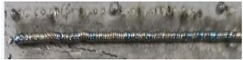 | 160 | 2.4 |
| 3 | 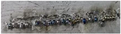 | 160 | 2.8 |
| Material | m1 (g) | m2 (g) | ρ (g/cm3) | ρ0 (g/cm3) | Relative Density (%) |
|---|---|---|---|---|---|
| Ti-6Al-4V | 9.0851 | 6.9577 | 4.2705 | 4.371 | 97.7 |
Publisher’s Note: MDPI stays neutral with regard to jurisdictional claims in published maps and institutional affiliations. |
© 2022 by the authors. Licensee MDPI, Basel, Switzerland. This article is an open access article distributed under the terms and conditions of the Creative Commons Attribution (CC BY) license (https://creativecommons.org/licenses/by/4.0/).
Share and Cite
Li, S.; Ma, K.; Xu, C.; Yang, L.; Lu, B. Numerical Analysis and Experimental Verification of Resistance Additive Manufacturing. Crystals 2022, 12, 193. https://doi.org/10.3390/cryst12020193
Li S, Ma K, Xu C, Yang L, Lu B. Numerical Analysis and Experimental Verification of Resistance Additive Manufacturing. Crystals. 2022; 12(2):193. https://doi.org/10.3390/cryst12020193
Chicago/Turabian StyleLi, Suli, Kaiyue Ma, Chao Xu, Laixia Yang, and Bingheng Lu. 2022. "Numerical Analysis and Experimental Verification of Resistance Additive Manufacturing" Crystals 12, no. 2: 193. https://doi.org/10.3390/cryst12020193
APA StyleLi, S., Ma, K., Xu, C., Yang, L., & Lu, B. (2022). Numerical Analysis and Experimental Verification of Resistance Additive Manufacturing. Crystals, 12(2), 193. https://doi.org/10.3390/cryst12020193