Abstract
A LiNbO3 integrated optics sensor fusing with an optical waveguide Mache–Zehnder interferometer (MZI), a loop-antenna, and a segmented electrode has been proposed, designed, and fabricated for the measurement of pulsed current. The experiment results have demonstrated that, for measurement of the standard 8/20 μs lightning pulsed current, the average of the front time and duration time of the sensor detected pulsed current waveform are 7.00 μs and 19.78 μs, respectively, while those detected by the Person CT are 7.30 μs and 20.35 μs, respectively. From 100 A to 3300 A, the sensor shows good linear characteristics, and the correlation coefficient is 0.9989. Moreover, the minimum detectable pulsed current is about 66 A in the time domain. All these results reveal the sensor can provide a new and potential technology for the measurement of pulsed current in the time domain.
1. Introduction
The time domain measurement of high-level pulsed current plays an important role regarding research of the electromagnetic effect and protection [1]. A traditional current transformer (CT) is not adequate because of saturation in a large current [2]. Due to the absence of a magnetic core, a Rogowski coil has the advantages of a large measurement range, wide bandwidth, and excellent transient response, which results in it being an optimal choice for measuring the fast large pulsed current [3,4,5,6,7,8]. However, as the measured current is proportional to the derivative of the magnetic flux, an integrator is required to retrieve the pulsed current waveform, and the direct current (DC) component could not be detected. Recently, a new current measurement method with a tiny printed circuit board (PCB) Rogowski coils sensor embedded in an insulated-gate bipolar transistor (IGBT) module has been proposed to measure the DC component by picking up a switching current flowing through an IGBT chip [9,10,11]. Besides, a measuring system based on PCB Rogowski coils for the measurement of a multi-split high current has been developed to convert the engineering problem into a mathematical one that could be solved through calculation, which results in the harmonic suppression system having been simplified [12]. However, for high-level current measurement, the high voltage non-insulated and electromagnetic interference (EMI) problems cannot be ignored.
Compared with traditional CT and Rogowski coils, the fiber optic current sensor (FOCS) has the advantages of high immunity to EMI, good electrical isolation, and wider frequency response [13,14]. As the current measurement is implemented by calculating the circular-birefringence-caused phase difference resulting from the Faraday Effect, the measurement accuracy relies on the stability of the Verdet constant and polarization characteristics, which can be easily influenced by environmental disturbance. To improve stability, considerable efforts, including using a highly twisted low-birefringence fiber, utilizing a dual wavelength configuration, optimizing initial phase delay in the λ/4 wave plate, utilizing a coil of spun highly birefringent fiber, self-compensative with two sensing heads, using two toroidal permanent magnets, and other techniques, have been developed [15,16,17,18,19,20]. However, the problem has not been solved completely, but the sensor structure becomes more complex to some extent. In comparison with the FOCS, the fiber Bragg grating (FBG)-based current sensor has the advantages of no polarization maintaining fiber (PMF) and discrete optical components, and it is capable to implement the multi-point measurement by cascading a series of sensors in one optical fiber [21,22,23,24,25,26,27]. However, the cross-sensitivity to temperature of FBG is a problem that should be solved. Recently, by applying opposite bias to make the two FBGs, or by bonding two FBGs on two giant magnetostrictive materials with orthogonal magnetostriction directions, the influence caused by ambient temperature can be effectively eliminated [28,29]. However, the effectiveness of eliminating the temperature effects depends on the consistency of the two FBGs, which is usually difficult to meet. Besides, to improve the stability and precision, an FBG-based optical current sensor using a dual-loop optoelectronic oscillator has been designed [30]. However, the response speed is limited by the hysteresis effect of the magnetostrictive materials, which results in a sensor that is not able to be used to measure the pulsed current with a fast pulse front.
In this paper, a LiNbO3 integrated optics sensor that consists of an optical waveguide Mache–Zehnder interferometer (MZI) fused with a loop-antenna and segmented electrode has been proposed, designed, fabricated, and experimentally demonstrated for the measurement of pulsed current in the time domain. As the pulsed current is modulated on the lightwave based on the electro-optic (EO) effect of the lithium niobate (LN) crystal, the sensor has a sufficiently fast response that can be used to measure the time domain waveform of the fast pulsed current. All the theoretical, simulation, and experimental results reveal that the proposed sensor has the potential capability to be used for the measurement of fast pulsed current.
2. Sensor Principles and Fabrication
2.1. Sensing System
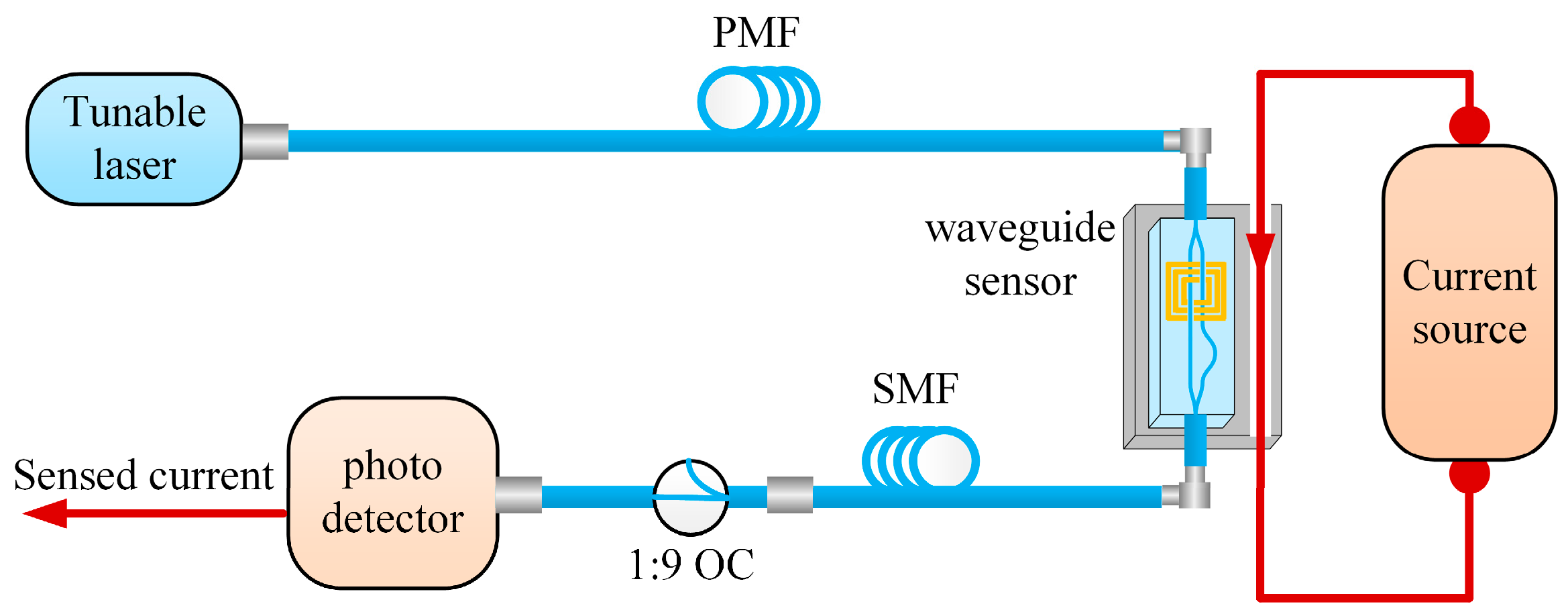
Figure 1 shows the schematic diagram of the measurement system for measuring the pulsed current based on the proposed integrated optics sensor. As can be seen, the output linear polarized light beam from the tunable laser is transmitted to the integrated optical waveguide current sensor by using the PMF. The sensor and the current-carrying wire are installed on the same insulation seat. When the electric current under measurement travels through the carrying wire, a variable magnetic field is generated and passes through the loop-antenna of the sensor. Based on Faraday’s law of electromagnetic induction, an induced voltage is generated on the two parallel electrodes, which are connected with the loop-antenna. Based on the EO effect of the LN crystal, the light beam travelling through the optical waveguide is modulated by the induced voltage, which causes the electric current to be modulated onto the optical carrier. At the receiving end, the output optical signal from the senor is transmitted to the photo detector (PD, Beijing Safety Test Technology Co., Ltd., Beijing, China) to convert into an electrical one by using the single mode fiber (SMF, Shenzhen Oscom Technology Co., Ltd., Shenzhen, China). The pulsed current is finally obtained by extracting the electrical signal using an existing instrument, such as an oscilloscope. However, for the measurement system, the wavelength of the tunable laser is tuned to ensure that the sensor can work in the linear area of its transmission curve. The more detailed principles of this operation point control technique have been presented in the previous work [31].
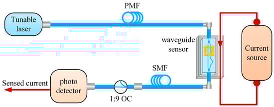
Figure 1.
The schematic diagram of the current sensing system.
2.2. Sensor Structure and Operation Principles
The physical structure of the proposed integrated optics pulsed current sensor is shown in Figure 2.
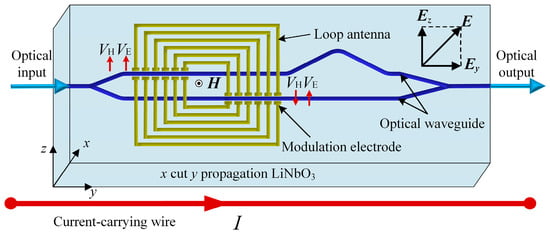
Figure 2.
Physical structure of the proposed integrated optics current sensor.
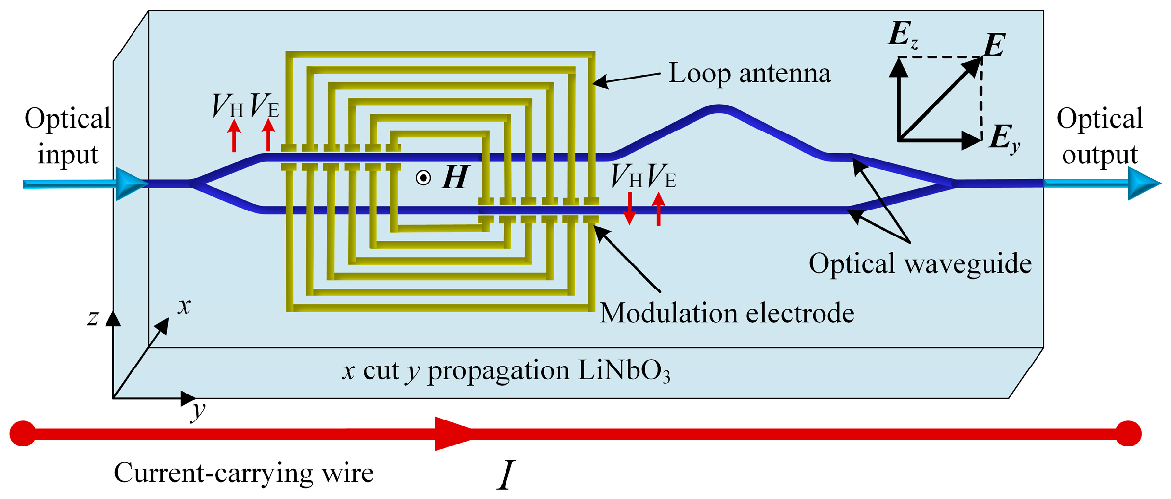
As can be seen from Figure 2, the proposed integrated optics pulsed current sensor consists of an integrated optical waveguide MZI, two parallel modulation electrodes, and a loop-antenna. The waveguide, electrode, and antenna are all fabricated on the same x cut y propagation LN substrate. The current-carrying wire is parallel with the y axis of the LN crystal. The distance between the loop-antenna and the current-carrying wire is as small as possible to improve the measurement sensitivity.
With the distance between the current-carrying wire and the loop-antenna r satisfied with r ≪ λ (λ is wavelength of the current travelling in the current-carrying wire), the magnetic field H induced by the current I can be written as
where μ = μ0μr is permeability, μ0 is the permeability in vacuum, and μr is the relative permeability. Under an electrically small loop condition, the loop-antenna can be represented by an equivalent circuit [32], and the voltage VH applied to the electrode can be expressed as
where L is the self-inductance of the loop-antenna, CLN is the capacitance of the parallel electrode with the LN crystal, ω is the current angular frequency, and S is area enclosed by the loop-antenna. Therefore, based on the EO effect of the LN crystal, the phase difference of the lightwave caused by the induced voltage can be described as
where λ is the optical wavelength of the input light beam, neff is effective refractive index of the optical waveguide, γ33 is EO coefficient of the LN crystal, Lel and Gel are length and gap of the parallel modulation electrodes, respectively, and Г (<1) is the overlap factor between the optical and electrical field. When φ(V) = π, the half-wave voltage Vπ can be written as
As shown in Figure 2, with the magnetic field H penetrating perpendicularly into the aperture of the loop-antenna, an electric field E = (Ez, Ey) perpendicular to H appears on the electrode. Thus, the same voltage VEz induced by Ez appears on both the right and left electrode, while the voltage VEy induced by Ey does not modulate the lightwave travelling through the optical waveguide (TE mode, polarized along the z axis). Thus, the phase difference of the lightwave travelling through the two arms of the optical waveguide MZI can be written as
Based on the fundamental theory of the integrated optical waveguide MZI modulator [33], the output optical power of the sensor can be described as
where Pin is the input optical power, α is the insertion loss, b is the extinction coefficient of the MZI, and φ0 is the static phase difference (operation point) of the MZI with no electric field. Considering an asymmetric MZI is designed and used for the proposed sensor, and the static phase can be changed with change of external conditions, such as the temperature, humidity, and stress, φ0 can be written as
where neff is the effective refractive index, ΔL stands for the length difference of the two arms of the optical waveguide MZI, and Δφ0 stands for the phase shift caused by the change in external environment conditions. Based on the previous work, by controlling wavelength of a tunable laser, it is possible to control the operation point return to the linear area of the transmission cure (φ0 = π/2) of the MZI type sensor [31]. Therefore, 2πVH/Vπ is small, and φ0 = π/2, assuming A = αPin/2, B = 2Aπb/Vπ, (6) can be simplified as
According to (8), the electric current under measurement is linear with output optical power of the sensor, and, by using a PD to convert the output optical signal into electrical, the electric current can be measured.
2.3. Sensor Design and Fabrication
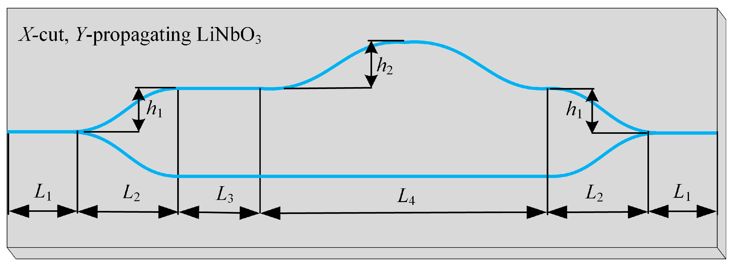
The physical structure of the designed integrated optical waveguide asymmetric Mache–Zehnder interferometer (AMZI) is shown in Figure 3. As can be seen, the AMZI consists of the input/output Y branch, the two parallel optical waveguide L3, the straight optical waveguide L4, and the bend optical waveguide (with bend height being h2). The two parallel optical waveguide is designed and used to ensure the symmetry of the right and left electrode fabricated around them, which results in the modulation effect caused by VE being able to be cancelled. To reduce optical loss and to generate an intrinsic static optical phase difference, the s shaped bend waveguide arm is designed. Then, the arm length difference ΔL of the AMZI can be calculated by

Figure 3.
Physical structure of the integrated optics AMZI.
According to (9), the parameters of the bend optical waveguide length L4 and height h2 are designed as 33 mm and 674.6 μm, respectively, to make the arm length difference ΔL of the AMZI about 34 μm. Thus, the change in static optical phase difference of the sensor is approximately equal to 2π under the condition of the optical wavelength tuned from 1530 nm to 1565 nm (C band). As a result, the operation point can be controlled effectively to the linear area when the static phase difference varies with the change in the external conditions. The detailed descriptions of the control method can be found in the previous work [31].
Under the condition of the practical fabrication process, length, width, and thickness of the used LN substrate are 50,000 μm, 4100 μm, and 500 μm, respectively. Length of the input and output waveguide L1 is designed as 5000 μm to ensure the fiber coupled input light beam can form a stabilized transmission mode before it is split in the Y branch. Besides, the length and height of the Y branch L2 and h2 are designed as 1500 μm and 11 μm to decrease the bend loss and simultaneously avoid the optical coupling between the two arms of the Y branch. As a result, L3 is designed as 4000 μm.
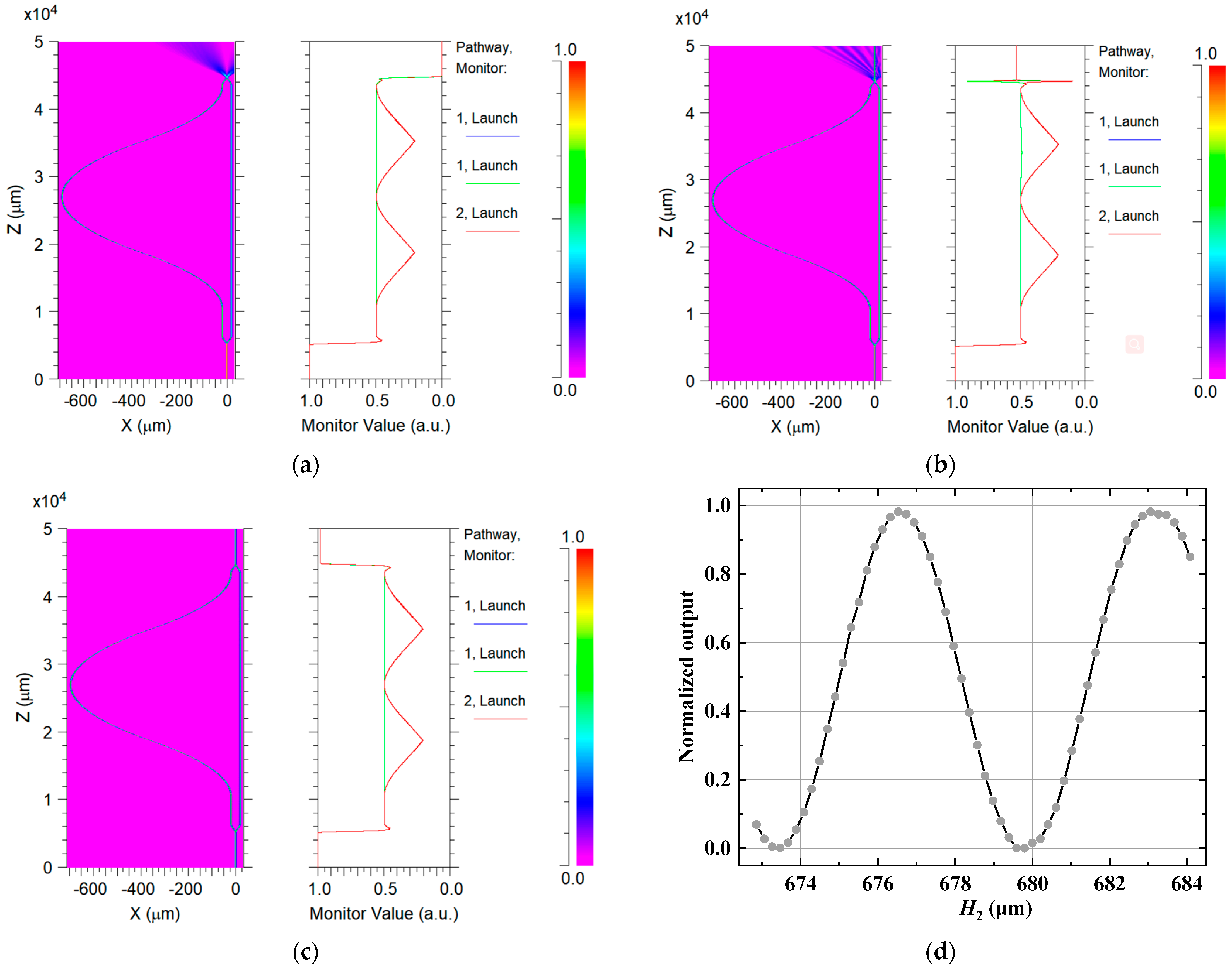
Consider the insertion loss of the optical waveguide AMZI being mainly decided by the bend height, h2, with the aforementioned parameters, and the physical model of the waveguide AMZI being set up based on the Rsoft computer aided design (Rsoft-CAD). To ensure single mode transmission operating at 1.5 μm, the width of the optical waveguide is designed as 6 μm. The transmission characteristics are simulated with the bend height changed from 673 μm to 684 μm, corresponding to the length difference of the two arms of the AMZI, which varied from 33.84 μm to 34.95 μm; the results are shown in Figure 4. From Figure 4, it is clear that the incident lightwave is almost equally split at the input Y-branch, and the scattering and radiation loss definitely exist at the bend corner. With h2 changed from 673 μm to 684 μm, the normalized optical power first decreased and then increased. Therefore, the bend height h2 is designed as 676.5 μm, and then the normalized output is 98.2%. The detailed parameters of the designed AMZI optical waveguide are shown in Table 1.
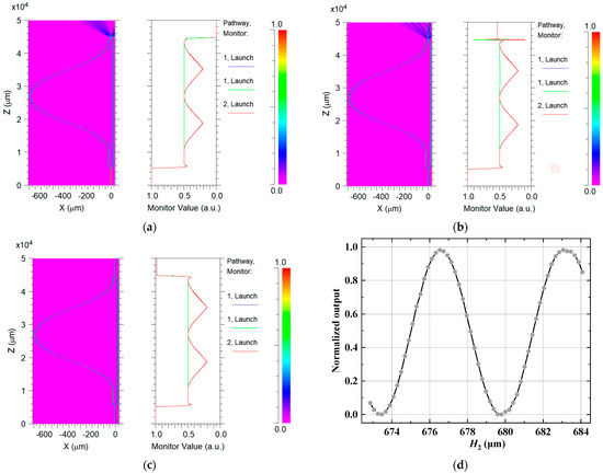
Figure 4.
Transmission characteristics of the optical waveguide AMZI: (a) H2 = 673.5 μm; (b) H2 = 675.1 μm; (c) H2 = 676.5 μm; (d) normalized output under different h2.

Table 1.
The parameters of the designed AMZI.
However, because the simulation results are carried out under the condition of the refractive index of the substrate and optical waveguide being absolutely homogeneous, which can hardly meet the practical fabricated optical waveguide, the simulation results are only for reference in optical waveguide designing.
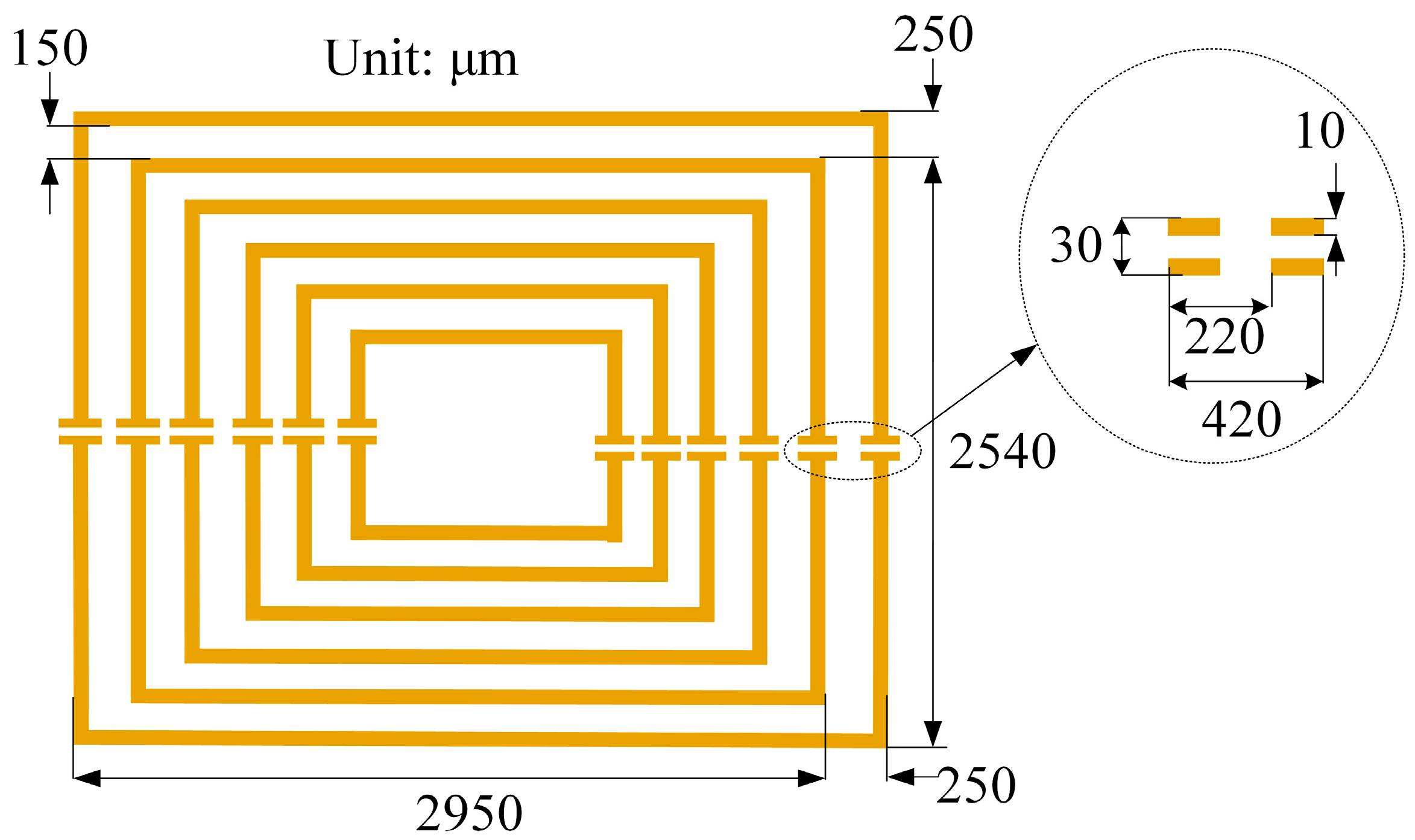
As shown in Figure 5, in order to improve sensitivity of the sensor, a multi-loop-antenna incorporated with segmented electrode has been designed and used to maximize the induced voltage as well as the EO interactive length. Consequently, according to (2) and (3), the optical phase difference of the lightwave travelling through the optical waveguide can then be rewritten as
where Гn (<1) is the overlap factor between electric field and optical field for the n-th electrode, Sn is the area enclosed by the n-th loop-antenna, and Lnel and Gnel are the gap and length of the n-th electrode. From (10), by using the multi-loop-antenna and the segmented electrode, the optical phase difference caused by the current under measurement has been increased effectively.

Figure 5.
Geometric dimensions of the loop-antenna and segmented electrode.
As shown in Figure 2, to eliminate the effect of the electric field VE, two (the left and right) identical groups of segmented electrodes are designed and fabricated between the two parallel optical waveguide arms (L3) to generate symmetric modulation. Therefore, considering the length (L3) and distance (2h1) of the parallel optical waveguide arms are 4000 μm and 22 μm, respectively, the vertical distance between the left and right electrode is designed as 28 μm and length of the square loop-antenna is designed as 3200 μm. Besides, considering the width of the LN substrate is 3000 μm, width of the square loop-antenna is designed as 2790 μm. The gap between the two parallel electrodes is designed as 10 μm to facilitate position alignment with the 6 μm width single mode optical waveguide. The geometric dimensions of the loop-antenna and segmented electrode are shown in Figure 5.
With the aforementioned parameters, the loop-antenna, segmented electrode, and optical waveguide AMZI are established on an LN substrate with dimensions of 48 × 3 × 0.5 mm3 based on the COMSOL MULITI-PHYSICS. The magnetic field module is used to generate a sinusoidal current with amplitude of 50 A on the current-carrying wire. Considering the distance between the sensor package edge and the LN substrate center is about 7 mm and thickness of the package edge is 2 mm, the distance away from the current-carrying wire to the center of the loop-antenna is designed as r = 10 mm to generate larger magnetic induction. As a result, the larger magnetic flux is generated by the loop-antenna and larger induced voltage is generated on the segmented electrode, yielding a higher measurement sensitivity. The magnetic field distributions are simulated and shown in Figure 6a. As can be seen, the magnetic field is mainly concentrated around the current carrying-wire. Moreover, Figure 6b,c shows the electric field distributions on the left and right segmented electrode, respectively. As can be seen, the induced electric field on the outer electrode (connecting with the outer loop of the multi-loop-antenna) is obviously larger than that on the inner electrode. This comes from the fact that the area of the outer loop-antenna is larger, which results in a larger magnetic flux. The electric field on the left electrode (across the upper optical waveguide of the two parallel waveguide arms) is along the +z direction, while the electric field on the right electrode (across the lower optical waveguide of the two parallel waveguide arms) is along the −z direction. Therefore, a push–pull modulation is generated by the magnetic-field-induced differential voltage.
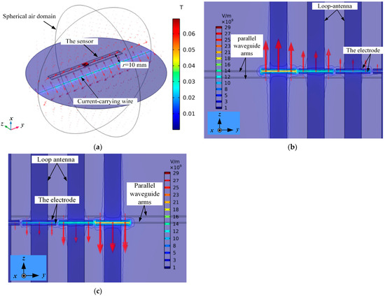
Figure 6.
Transmission characteristics of the optical waveguide AMZI: (a) the magnetic field distribution; (b) the electric field distribution on the left electrode; (c) the electric field distribution on the right electrode.
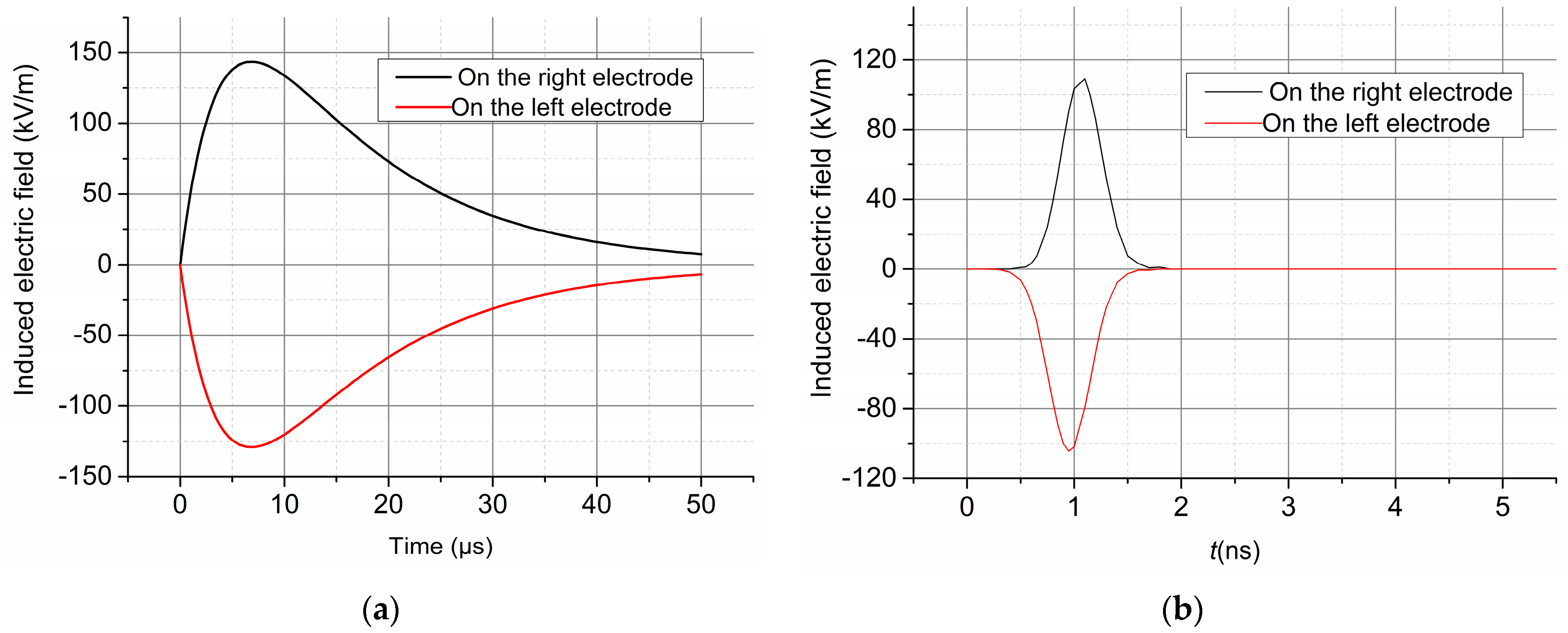
In order to show the time domain response of the sensor under pulsed current, a double exponential pulse current (I(t) = I0k(e−αt − e−βt), α = 7.714 × 10⁴, β = 2.489 × 10⁵, k = 2.33, I0 = 100 A) with wave front time Tf = 5.55 µs and duration time Td = 21.12 µs, and a Gaussian pulse current (I(t) = I0exp(−4π(t − t0)2/τ2), τ = 1 ns, I0 = 100 A) with rise time Tf = 1.0 ns and pulse width Td =1 ns are applied to the current-carrying wire. The induced electric field on the left and right modulation electrode are detected by using the electric field probe. The results are shown in Figure 7a,b, respectively. From Figure 7a, the front and duration time of the detected exponential pulse current waveform on the right and left electrode are 4.90 μs/21.83 μs and 4.88 μs/22.42 μs, respectively. From Figure 7b, the rise time and pulse width of the detected Gaussian pulse current on the right and left electrode are 0.8 ns/1.0 ns and 0.9 ns/1.1 ns, respectively. As a result, the detected induced electric field on the electrode agrees well with the applied pulsed current. Besides, directions of detected pulsed electric field on the right and left electrode are reverse, which is consistent with the theoretical analysis results.
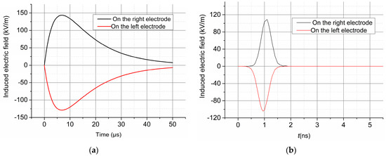
Figure 7.
Simulation results for the time domain response of the sensor under (a) double exponential pulsed current; (b) Gaussian pulse current.
Furthermore, the equivalent circuit of the loop-antenna and parallel electrode has been shown in Figure 8. In Figure 8, Cm stands for the capacitance of the parallel electrodes, Lm and Rm are the inductor and resistance of the loop-antenna, and Va is the induced voltage. Based on the above simulation mode established using the COMSOL MULITI-PHYSICS, Lm and Cm of the loop-antenna and segmented electrode are calculated as 9.2834 nH and 0.12159 pF, respectively. Then, the limiting frequency bandwidth of the device can be estimated to be 1/2π√LmCm = 6.7 GHz.
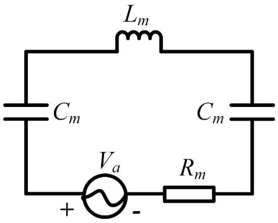
Figure 8.
Equivalent circuit of the loop-antenna and segmented electrode.
With the aforementioned parameters, the optical waveguide MZI integrated with the metallic loop-antenna and segmented electrode are fabricated on an x-cut y-propagating LN wafer crystal with diameter 3 inches and thickness 0.5 mm by the photolithographic technology. The optical waveguide is fabricated by the annealed proton exchange (APE) technology. Firstly, the waveguide is fabricated by proton exchanging in benzoic acid with a small amount of lithium and benzoate at 250 °C to 300 °C for 4.5 h, and then annealed in the furnace at 350 °C to 400 °C for 5 h. However, as the APE process results in the refractive index being noticeably increased for the extraordinary lightwave while the ordinary lightwave is unnoticeably decreased, the APE waveguide supports only the TE mode (polarized along the z axis). Therefore, the lightwave travelling through the optical waveguide can only be modulated by the electric field along the z axis. This is the reason why the voltage, VEy, induced by Ey does not modulate the lightwave. Besides, for this linear polarization characteristic, the PMF is used to couple with the input optical waveguide of the sensor to improve the lightwave coupling efficiency and working stability. However, as the lightwave interference has occurred at the output Y branch, only the SMF is used to couple with the output waveguide of the sensor to transmit the output optical power. Secondly, before fabricating the antenna and electrode, a SiO2 buffer layer with a thickness of ∼4000 Å is deposited upon the optical waveguide MZI by using the radio frequency (RF) magnetic sputtering so as to reduce the optical absorption loss that comes from the metallic electrode and antenna. Then, by sputtering Cr and Au and then electroplating Au, the segmented electrode and loop-antenna with a thickness of ∼5000 Å are fabricated among the two parallel waveguide arms of the MZI. The position of the electrode and antenna is about 8500 μm and 2050 μm along the longitudinal and horizontal of the LN wafer, respectively. The more detailed fabrication processes of the waveguide sensor have been shown in the previous work [34]. Finally, the sensor chip is cemented in a polypropylene packaging by using the silicone to improve its mechanical strength.
Figure 9 shows the photograph of a packaged integrated optics electric current sensor. As can be seen, the size of the packaged sensor is 78 mm × 15 mm × 10 mm. Moreover, in order to easily fix the current-carrying wire and to ensure the distance between the current wire and the loop-antenna is 10 cm in practical application, an insulated base with a groove has been fabricated and used.
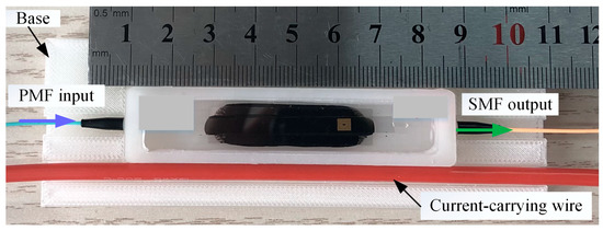
Figure 9.
Photograph of the packaged electric current sensor.
3. Experimental Results
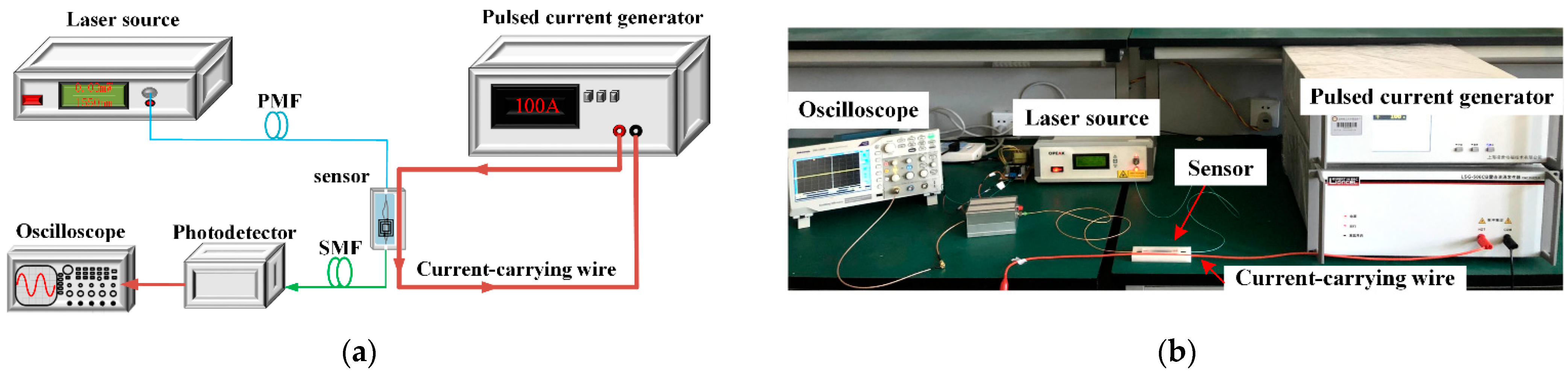
Figure 10 shows the experiment setup for the measurement of the pulsed current by using the fabricated integrated optics sensor.
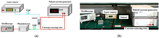
Figure 10.
Pulsed current measurement system: (a) schematic diagram; (b) photograph of the experimental setup.
From Figure 10a, the current-carrying wire is connected with the input and output port of the pulsed current generator (LSG-506 CB) to generate the 8/20 μs standard lightning current from 50 A to 3300 A. The current-carrying wire is embedded into the groove of the sensor base. The distance between the sensor and the current-carrying wire is 10 mm. The tunable laser with an output optical power of 10 dBm, tunable wavelength range from 1530 nm to 1565 nm, and channel spacing of 0.4 nm is connected with the sensor input port by the PMF. The output wavelength of the laser source is tuned to ensure the sensor works at the linear area of the transmission curve. The output optical power of the sensor is transmitted to the PD with a bandwidth of 100 MHz to convert into electrical. The oscilloscope with a sampling rate of 2 GS/s and bandwidth of 200 MHz (Tektronix MDO3024) is used to extract the waveform of the measured pulsed current.
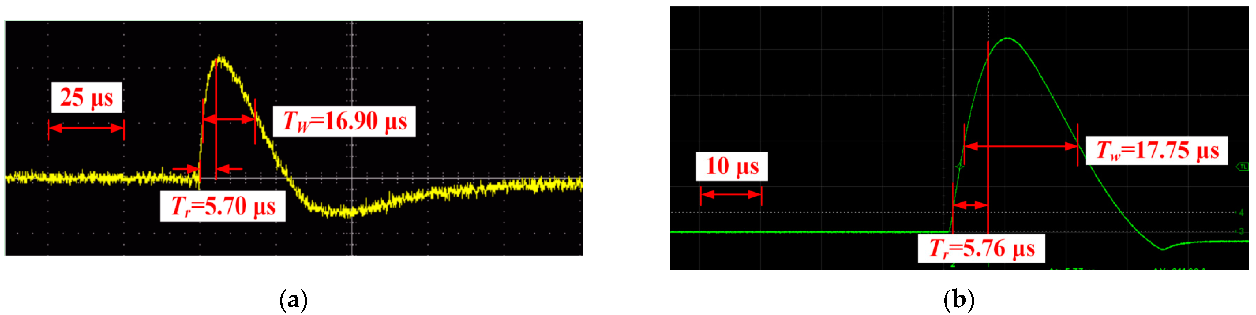
As an example, under the pulsed current of 2000 A, the sensor detected pulsed current waveforms are shown in Figure 11a. However, for comparison, the pulsed current is simultaneously measured by using the standard Pearson CT. From Figure 11a,b, the rise time, Tr, and pulse width, Tw, of the detected pulsed current waveforms using the proposed sensor and the Pearson CT are 5.70/16.90 μs and 5.76/17.75 μs, respectively. According to the standard of electromagnetic compatibility testing and measurement techniques surge immunity test (GB/T 17626.5-2019/IEC 61000-4-5: 2014), the front time Tf = 1.25 × Tr and duration time Td = 1.18 × Tw are 7.13/19.94 μs and 7.21/20.97 μs, respectively.
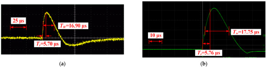
Figure 11.
Time domain response, pulsed current measurement system: (a) time domain response of the proposed sensor; (b) time domain response of the Pearson CT.
For comparative analysis, the parameters of the front time and duration time of the detected pulsed current with different peak amplitudes by using the proposed sensor and the Pearson CT are shown in Table 2. From Table 2, the values for the pulsed current are 100 A, 1000 A, 2000 A, and 3300 A; the average front time, Tf, and duration time, Td, of the detected pulsed current waveforms by using the Pearson CT and the proposed optical waveguide sensor are 7.30/20.35 μs and 7.00/19.78 μs, respectively. In comparison with the output standard lightning pulsed current (Tf = 8 ± 20% μs, Td = 20 ± 20% μs) from the pulsed current generator, the average relative errors are 8.7%/1.7% and 12.5%/1.1%, respectively. As a result, the proposed sensor has the potential capability to be used to measure the pulsed current in the time domain.
Table 2.
Waveform parameters comparison of the pulsed current measured by optical waveguide sensor and Pearson CT.
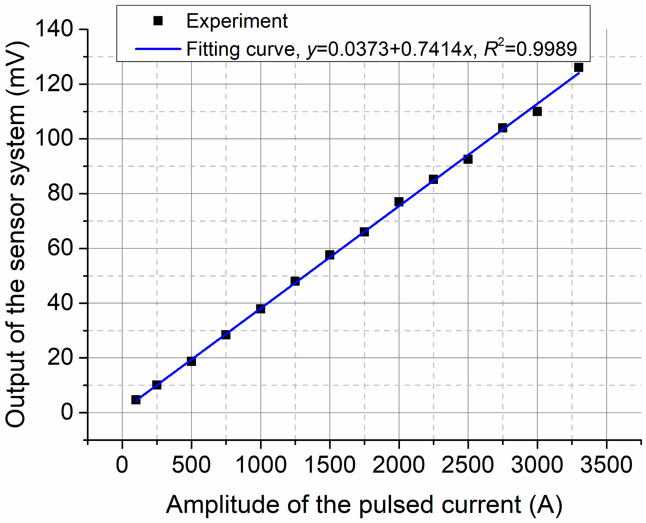
In addition, in order to demonstrate the input/output characteristics of the sensor, with the output pulsed current changed from 100 A to 3300 A by a step of 250 A, the amplitudes of the sensor system output signals are measured and shown in Figure 12. A linear fitting curve y = 0.0373 + 0.7414x is used to stand for the relationship between the input pulsed current and the output of the sensor system. The linear correlation coefficient of 0.9989 reveals that the sensor has a better linear characteristic. Moreover, in the experiment, considering the noise floor of the sensor system is about 1.6 mV, the minimum detectable current of the sensor system is about 66 A under the condition of the signal to noise ratio (SNR) being 6 dB.
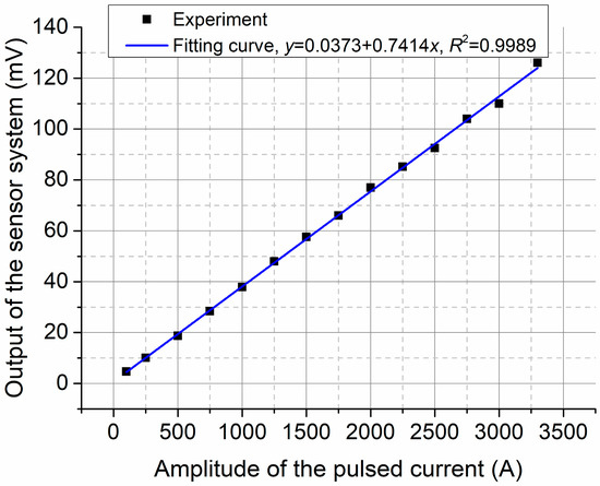
Figure 12.
Input/output characteristics of the sensor.
4. Conclusions
In summary, a LiNbO3 integrated optics sensor for the measurement of pulsed current has been proposed, fabricated, and measured. By fabricating the multi-loop-antenna and segmented electrodes around the LN optical waveguide MZI, the lightwave travelling through the optical waveguide can be modulated by the electric current under measurement based on Faraday’s law of electromagnetic induction and the EO effect of the LN crystal. In comparison with the traditional CT, Rogowski, fiber optical sensor, or FBG-based current sensor, this new type of sensor has the advantages of good immunity to EMI, no integrator required, fast response, small and compact structure, and being convenient to implement. The experimental results demonstrate that, for measuring the standard lightning pulsed current travelling through the current-carrying wire, the current waveform detected by the proposed sensor shows good consistency with that detected by the standard Pearson CT. Besides, in the range of 100 A to 3300 A, the sensor has better linear characteristics, with the linear correlation coefficient being 0.9989. The minimum detectable current is about 66 A, while the maximum detectable current is more than 3300 A. All these results demonstrate the proposed sensor can provide a new and potential technology for measuring pulsed current.
Author Contributions
Conceptualization, J.Z. (Jing Zhang); methodology, J.Z. (Jiahong Zhang); software, Y.L.; validation, J.Z. (Jing Zhang) and Y.L.; formal analysis, J.Z. (Jing Zhang) and J.Z. (Jiahong Zhang); investigation, J.Z. (Jing Zhang) and Q.L.; resources, J.Z. (Jing Zhang) and Y.L.; writing—original draft preparation, J.Z. (Jiahong Zhang) and Q.L.; writing—review and editing, J.Z. (Jiahong Zhang) and Q.L.; visualization, J.Z. (Jing Zhang) and Q.L.; supervision, J.Z. (Jing Zhang) and Y.L.; project administration, J.Z. (Jiahong Zhang) and Y.L.; funding acquisition, J.Z. (Jiahong Zhang) and Y.L. All authors have read and agreed to the published version of the manuscript.
Funding
This work is funded by the National Natural Science Foundation of China 62162034, 61962031, the Yunnan Province Basic Research Program Key Project 202101AS070016, the 2020 Yunnan Province Graduate Quality Course “Algorithm Analysis and Design” Construction Project 109920210048, the Yunnan Province “Ten Thousand Talents Program” Industrial Technology Leading Talent Project Yfgr [2019] No. 1096, and the Yunnan Province Technological Innovation Talent Project 2019HB113.
Institutional Review Board Statement
Not applicable.
Informed Consent Statement
Informed consent was obtained from all subjects involved in the study.
Data Availability Statement
Not applicable.
Acknowledgments
The contributions of all my co-authors are gratefully acknowledged.
Conflicts of Interest
The authors declare no conflict of interest.
References
- Li, W.; Mao, C.; Lu, J. Study of the Virtual Instrumentation Applied to Measure Pulsed Heavy Currents. IEEE Trans. Instrum. Meas. 2005, 54, 284–288. [Google Scholar] [CrossRef]
- Ziegler, S.; Woodward, R.C.; Iu, H.H.-C.; Borle, L.J. Current Sensing Techniques: A Review. IEEE Sens. J. 2009, 9, 354–376. [Google Scholar] [CrossRef]
- Pellinen, D.G.; Di Capua, M.S.; Sampayan, S.E.; Gerbracht, H.; Wang, M. Rogowski coil for measuring fast, high-level pulsed currents. Rev. Sci. Instrum. 1980, 51, 1535–1540. [Google Scholar] [CrossRef]
- Ramboz, J.D. Machinable rogowski coil, design, and calibration. IEEE Trans. Instrum. Meas. 1996, 45, 511–515. [Google Scholar] [CrossRef]
- Gerasimov, A.I. Wide-Range Inductive Sensors of Currents with Nanosecond Rise Times for Measuring Parameters of High-Current Pulses (Review). Instrum. Exp. Tech. 2002, 45, 147–161. [Google Scholar] [CrossRef]
- Liu, Y.; Lin, F.; Zhang, Q.; Zhong, H. Design and construction of a Rogowski Coil for measuring wide pulsed current. IEEE Sens. J. 2011, 11, 123–130. [Google Scholar] [CrossRef]
- Zhang, W.; Sohid, S.B.; Wang, F.; Cui, H.; Holzinger, B. High-Bandwidth Combinational Rogowski Coil for SiC MOSFET Power Module. IEEE Trans. Power Electron. 2022, 37, 4397–4405. [Google Scholar] [CrossRef]
- Fu, S.; Deng, E.; Peng, C.; Zhang, G.; Zhao, Z.; Cui, X. Method of Turns Arrangement of Noncircular Rogowski Coil with Rectangular Section. IEEE Trans. Instrum. Meas. 2021, 70, 1–10. [Google Scholar] [CrossRef]
- Hasegawa, K.; Takahara, S.; Tabata, S.; Tsukuda, M.; Omura, I. A new output current measurement method with tiny PCB sensors capable of being embedded in an IGBT module. IEEE Trans. Power Electron. 2017, 32, 1707–1712. [Google Scholar] [CrossRef] [Green Version]
- Hasegawa, K.; Sho, S.; Tsukuda, M.; Omra, I.; Ichiki, M.; Kato, T. Output-Current Measurement of a PWM Inverter with a Tiny PCB Rogowski Sensor Integrated into an IGBT Module. In Proceedings of the IEEE Energy Conversion Congress and Exposition, ECCE, Baltimore, MD, USA, 29 September–3 October 2019; pp. 5707–5711. [Google Scholar] [CrossRef]
- Bayarkhuu, B.; Bat-Ochir, B.; Hasegawa, K.; Tsukuda, M.; Dugarjav, B.; Omura, I. Analog Basis, Low-Cost Inverter Output Current Sensing with Tiny PCB Coil Implemented inside IPM. In Proceedings of the 2019 31st International Symposium on Power Semiconductor Devices and ICs (ISPSD), Shanghai, China, 19–23 May 2019; pp. 251–254. [Google Scholar] [CrossRef]
- Gu, P.Y.; Chen, Q.; Li, H.B.; Hu, C.; Gong, H.; Jiao, Y. PCB Rogowski Coils for 300 kA Current Measurement on a Multi-Split Conductor. IEEE Sens. J. 2019, 19, 6786–6794. [Google Scholar] [CrossRef]
- Belal, M.; Song, Z.; Jung, Y.; Brambilla, G.; Newson, T.P. Optical fiber microwire current sensor. Opt. Lett. 2010, 35, 3045. [Google Scholar] [CrossRef] [PubMed]
- Zhang, H.; Dong, Y.; Leeson, J.; Chen, L.; Bao, X. High sensitivity optical fiber current sensor based on polarization diversity and a Faraday rotation mirror cavity. Appl. Opt. 2011, 50, 924–929. [Google Scholar] [CrossRef] [PubMed]
- Bohnert, K.; Gabus, P.; Nehring, J.; Brändle, H. Temperature and vibration insensitive fiber-optic current sensor. J. Lightwave Technol. 2002, 20, 267–276. [Google Scholar] [CrossRef]
- Liu, T.; Han, J.; Hu, H. Optical Current Sensor with Dual-Wavelength Configuration for Improving Temperature Robustness. IEEE Photonics J. 2017, 9, 1–10. [Google Scholar] [CrossRef]
- Hu, H.; Huang, J.; Xia, L.; Yan, Z.; Peng, S. The compensation of long-term temperature induced error in the all fiber current transformer through optimizing initial phase delay in λ/4 wave plate. Microw. Opt. Technol. Lett. 2019, 61, 1769–1773. [Google Scholar] [CrossRef]
- Muller, G.M.; Frank, A.; Yang, L.; Gu, X.; Bohnert, K. Temperature Compensation of Interferometric and Polarimetric Fiber-Optic Current Sensors with Spun Highly Birefringent Fiber. J. Lightwave Technol. 2019, 37, 4507–4513. [Google Scholar] [CrossRef]
- Huang, Y.; Xia, L.; Pang, F.; Yuan, Y.; Ji, J. Self-Compensative Fiber Optic Current Sensor. J. Lightwave Technol. 2021, 39, 2187–2193. [Google Scholar] [CrossRef]
- Jia, Q.; Han, Q.; Liang, Z.; Cheng, Z.; Hu, H.; Wang, S.; Ren, K.; Jiang, J.; Liu, T. Temperature Compensation of Optical Fiber Current Sensors with a Static Bias. IEEE Sens. J. 2022, 22, 352–356. [Google Scholar] [CrossRef]
- Mora, J.; Díez, A.; Cruz, J.L.; Andrés, M.V. Magnetostrictive sensor interrogated by fiber gratings for DC-current and temperature discrimination. IEEE Photonics Technol. Lett. 2000, 12, 1680–1682. [Google Scholar] [CrossRef]
- Satpathi, D.; Moore, J.A.; Ennis, M.G. Design of a Terfenol-D based fiber-optic current transducer. IEEE Sens. J. 2005, 5, 1057–1065. [Google Scholar] [CrossRef]
- Cremonezi, A.O.; Ferreira, E.C.; Filho, A.J.B.; Dias, J.A.S. A fiber bragg grating RMS current transducer based on the magnetostriction effect using a terfenol-D toroidal-shaped modulator. IEEE Sens. J. 2013, 13, 683–690. [Google Scholar] [CrossRef]
- De Nazaré, F.V.B.; Werneck, M.M. Compact optomagnetic Bragg-grating-based current sensor for transmission lines. IEEE Sens. J. 2015, 15, 100–109. [Google Scholar] [CrossRef]
- Dante, A.; Lopez, J.D.; Carvalho, C.C.; Allil, R.C.D.S.B.; Werneck, M.M. A Compact FBG-Based Magnetostrictive Optical Current Sensor with Reduced Mass of Terfenol-D. IEEE Photonics Technol. Lett. 2019, 31, 1461–1464. [Google Scholar] [CrossRef]
- Lopez, J.D.; Dante, A.; Bacurau, R.M.; Cremonezi, A.O.; Mok, R.W.; Carvalho, C.C.; Allil, R.C.D.S.B.; Ferreira, E.C.; Werneck, M.M. Fiber-Optic Current Sensor Based on FBG and Optimized Magnetostrictive Composite. IEEE Photonics Technol. Lett. 2019, 31, 1987–1990. [Google Scholar] [CrossRef]
- Lopez, J.D.; Dante, A.; Cremonezi, A.O.; Bacurau, R.M.; Carvalho, C.C.; Allil, R.C.D.S.B.; Ferreira, E.C.; Werneck, M.M. Fiber-Optic Current Sensor Based on FBG and Terfenol-D with Magnetic Flux Concentration for Enhanced Sensitivity and Linearity. IEEE Sens. J. 2020, 20, 3572–3578. [Google Scholar] [CrossRef]
- Yang, Y.; Yang, Q.; Ge, W.; Li, L. A Temperature-Insensitive AC Current Sensor Based on Two Opposite Bias Magnetic Circuits. IEEE Photonics Technol. Lett. 2016, 28, 2724–2727. [Google Scholar] [CrossRef]
- Han, J.; Hu, H.; Wang, H.; Zhang, B.; Song, X.; Ding, Z.; Zhang, X.; Liu, T. Temperature-Compensated Magnetostrictive Current Sensor Based on the Configuration of Dual Fiber Bragg Gratings. J. Lightwave Technol. 2017, 35, 4910–4915. [Google Scholar] [CrossRef]
- Xiao, D.; Wang, G.; Yu, F.; Liu, S.; Shao, L.; Wang, C.; Fu, H.; Shum, P.P.; Ye, T.; Wang, W. Highly Stable and Precise Demodulation of an FBG-Based Optical Current Sensor Using a Dual-Loop Optoelectronic Oscillator. J. Lightwave Technol. 2021, 39, 5962–5972. [Google Scholar] [CrossRef]
- Zhang, J.; Luo, C.; Zhao, Z. Design and Application of Integrated Optics Sensor for Measurement of Intense Pulsed Electric Field. J. Lightwave Technol. 2019, 37, 1440–1448. [Google Scholar] [CrossRef]
- Suzuki, E.; Arakawa, S.; Ota, H.; Arai, K.I.; Sato, R. Optical magnetic field probe with a loop antenna element doubly loaded with electrooptic crystals. IEEE Trans. Electromagn. Compat. 2004, 46, 641–647. [Google Scholar] [CrossRef]
- Alferness, R.C. Waveguide Electrooptic Modulators. IEEE Trans. Microw. Theory Tech. 1982, 30, 1121–1137. [Google Scholar] [CrossRef]
- Lu, H.; Li, Y.; Zhang, J. Design and Analysis of Broadband LiNbO3 Optical Waveguide Electric Field Sensor with Tapered Antenna. Sensors 2021, 21, 3672. [Google Scholar] [CrossRef] [PubMed]


Publisher’s Note: MDPI stays neutral with regard to jurisdictional claims in published maps and institutional affiliations. |
© 2022 by the authors. Licensee MDPI, Basel, Switzerland. This article is an open access article distributed under the terms and conditions of the Creative Commons Attribution (CC BY) license (https://creativecommons.org/licenses/by/4.0/).