Article

The Growth of Hexagonal Boron Nitride Quantum Dots on Polycrystalline Nickel Films by Plasma-Assisted Molecular Beam Epitaxy

1
Department of Materials Science and Engineering, National Dong Hwa University, Hualien 97401, Taiwan
2
Department of Mechanical Engineering, Institut Teknologi Padang, Padang 25143, Kp Olo, Indonesia
*
Author to whom correspondence should be addressed.
Crystals 2022, 12(3), 347; https://doi.org/10.3390/cryst12030347
Submission received: 17 February 2022 / Revised: 28 February 2022 / Accepted: 1 March 2022 / Published: 3 March 2022
(This article belongs to the Special Issue Confined Crystals, Quantum Dots, and Nano Crystals)

Abstract

:
In this report, quantum dots of hexagonal boron nitride (h-BN) were fabricated on the surface of polycrystalline Ni film at low growth temperatures (700, 750, and 800 °C) by plasma-assisted molecular beam epitaxy. Reflection high-energy electron diffraction could trace the surface condition during the growth and perform the formation of BN. The observation of surface morphology by scanning electron microscopy and atomic force microscopy showed the nanodots of BN on Ni films. The existence of crystal h-BN quantum dots was determined by the analysis of Raman spectra and Kevin probe force microscopy. The cathodoluminescence of h-BN quantum dots performed at the wavelength of 546 and 610 nm, attributed to the trapping centers involving impurities and vacancies. Moreover, the influence of temperatures for the substrate and boron source cell was also investigated in the report. When the k-cell temperature of boron and growth temperature of substrate increased, the emission intensity of cathodoluminescence spectra increased, indicating the better growth parameters for h-BN quantum dots.

1. Introduction

Boron nitride (BN) is a chemically stable material in the group III-V compounds, applied especially for electronic and optoelectronic devices [1,2]. Polymorphism of BN crystal structures include hexagonal (h-BN), rhombohedral (r-BN), turbostratic (t-BN), wurtzite (w-BN), and cubic (c-BN). h-BN has a similar structure to graphene with 1.7% lattice mismatch, as a two-dimensional (2D) material [3]. Excellent physical properties of h-BN include high thermal conductivity [4] and wide bandgap [5]. h-BN is not only a 2D material applied for electronic devices as an insulating layer or a quantum tunnel barrier, but it also has high potential for the applications in deep-ultraviolet light-emitting diodes (LEDs) [6].
For the fabrication of h-BN, several techniques have been employed to grow and produce h-BN. Ion beam sputtering deposition (IBSD) [7], metal organic chemical vapor deposition (MOCVD) [8], and plasma-assisted molecular beam epitaxy (PA-MBE) can be used for the growth of h-BN thin films [9,10,11]. Among them, PA-MBE has an exact growth control to produce high-quality epitaxy and at lower growth temperatures than others [12,13]. h-BN has also attracted attention for the growth on various substrates, such as Ni [10,14], graphene [15,16], cobalt [17,18], and sapphire [19,20].
Over the past few decades, semiconductor materials have been produced in low-dimensional nanostructures as quantum wells (2D), wires (1D), and dots (0D) to obtain novel devices by exploiting their quantum confinement effect. Quantum dots (QDs) are free-standing nanoparticles with nanometers. QDs have different optical and electronic properties from larger particles due to quantum mechanics [21]. QDs have unique properties for applications in batteries [22], LEDs [23], biosensors [24], and cancer therapy [25]. QDs of h-BN have a wide bandgap and excellent chemical stability at high temperatures. However, the study about h-BN quantum dots is infrequent so far.
In this work, we focus on the growth of h-BN QDs on the polycrystalline Ni substrates at a relatively low temperature by PA-MBE system. The characterizations of all samples were performed by using reflection high-energy electron diffraction (RHEED), field emission-scanning electron microscopy (FE-SEM), atomic force microscopy (AFM), Kelvin probe force microscopy (KPFM), Raman spectroscopy, and cathodoluminescence (CL) spectroscopy. This work also investigates the influence of substrate temperatures and Knudsen effusion cell (K-cell) temperatures of boron source on the growth of h-BN quantum dots.

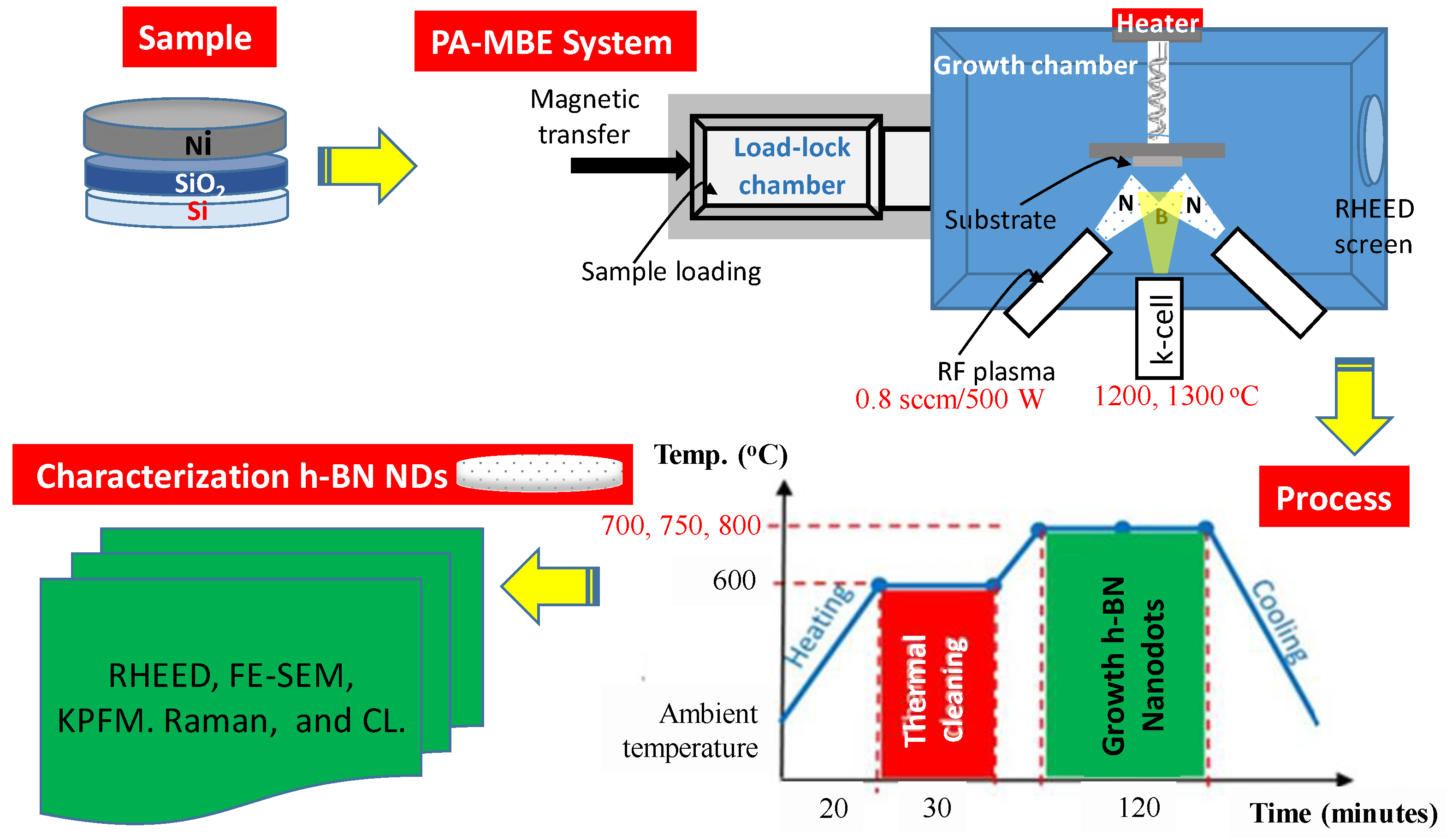
2. Materials and Methods

2.1. Preparation of Substrate

SiO2 film was formed on a polished and etched Si (100) wafer (Siltronix, 430 µm of thickness, and 2 inch of diameter) by an oxidation process. Then, a 100 nm-thick Ni film was deposited on SiO2 by an E-gun evaporator and annealed at 800 °C for 2 min to form Ni/SiO2/Si substrates.

2.2. The Growth of h-BN QDs

The growth of h-BN QDs on Ni/SiO2/Si substrate was conducted by a ULVAC PA-MBE system. The growth chamber was equipped with high-temperature K-cell as boron sources (UMAT, slug form, 99.9999%). 0.8 sccm high-purity nitrogen (99.9999%) was used as the nitrogen source, and radio frequency power was set to 500 W. Growth conditions of h-BN QDs at different K-cell and substrate temperatures are presented in Figure 1. The growth temperature for the substrate was varied from 700, 750, and 800 °C for 2 h [26]. All substrates were subjected to a thermal cleaning at 600 °C for 30 min to remove moisture and oxide on the surface before the growth of h-BN QDs. The base working pressure was 5 × 10⁻⁸ Pa. The K-cell temperature (TB) was set to 1200 and 1300 °C, respectively. B and N were generated simultaneously during the growth. After the growth process, samples were cooled down to an ambient temperature in the chamber.

2.3. Characterizations of h-BN Quantum Dots

The growth process was monitored by 20 kV in situ RHEED. After the growth of h-BN QDs, the surface morphology was examined by JEOL JSM-7000F FE-SEM equipped with a silicon-draft-detector-based energy dispersive X-ray spectroscopy (EDS). AFM and KPFM (Nanosurf C3000) were employed to measure the surface roughness and the local contact voltage as work functions of materials, respectively. Raman spectroscopy (Renishaw), equipped with a 532 nm laser, was used to check the h-BN QDs. The optical property of h-BN QDs was measured by cathodoluminescence (CL) spectroscopy coupled with scanning electron microscopy.

3. Results and Discussion

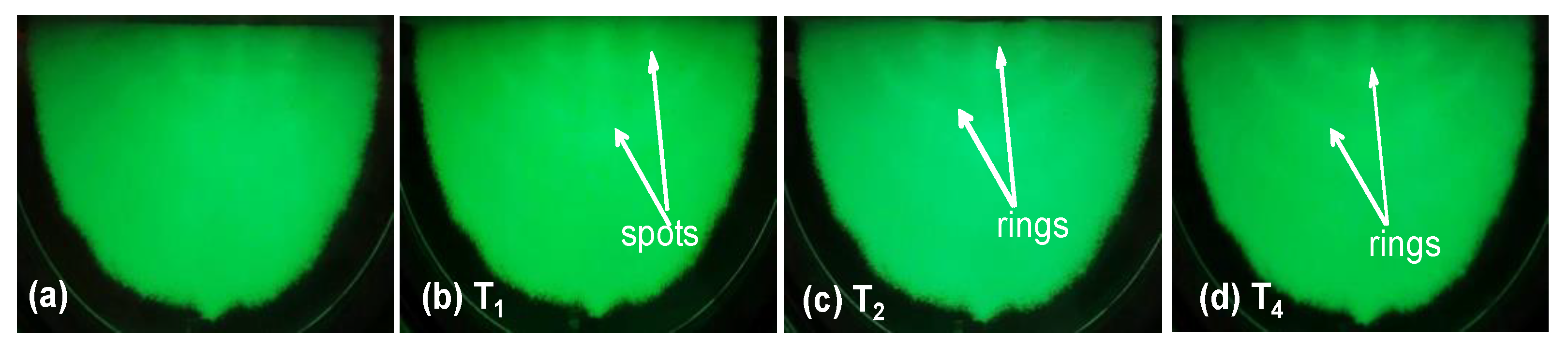
3.1. Reflection High-Energy Electron Diffraction

The PA-MBE is equipped with the RHEED to determine the substrate’s surface conditions and the growth of h-BN. Figure 2a is the RHEED pattern after thermal cleaning, and it looks spotty [27]. The pattern indicates that the substrate’s surface quality improved as the contamination was removed [28]. When the K-cell temperatures increase from 1200 to 1300 °C with 700 °C growth temperatures in Figure 2b,c, the RHEED pattern changed from spotty to rings pattern during the growth of h-BN. Furthermore, the ring pattern was apparent when the growth temperatures increased from 700 °C to 800 °C in Figure 2c,d. The ring-type pattern indicates the polycrystalline Ni surface with h-BN.

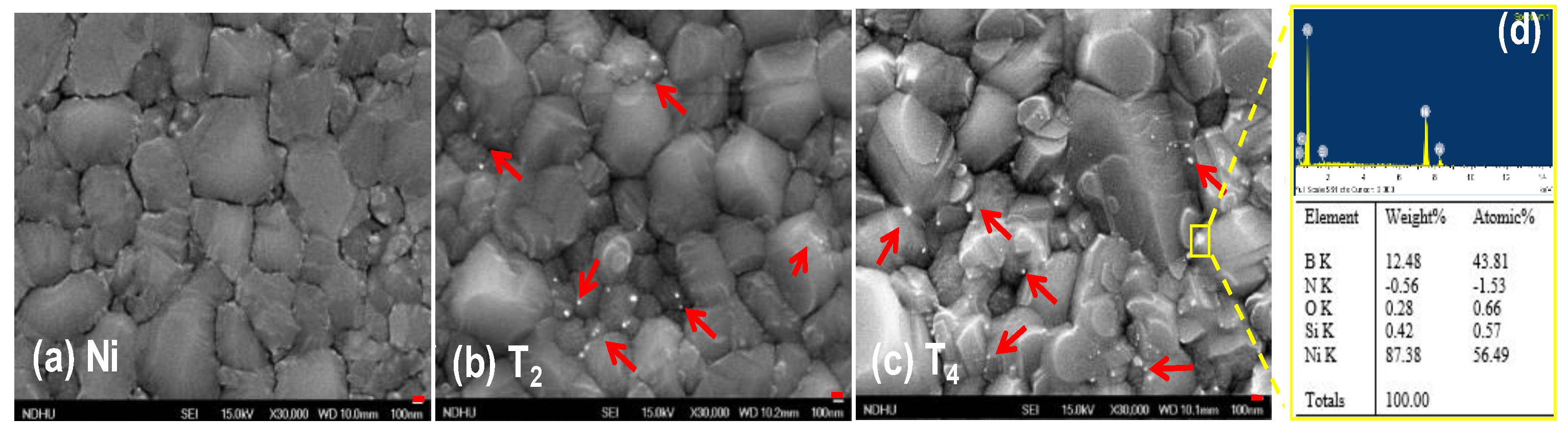
3.2. Field Emission-Scanning Electron Microscopy

FE-SEM was used to observe the surface morphology of samples. Figure 3a shows the polycrystalline Ni film with a rough surface and more grain boundary as reference. Samples T2 and T4 are the growth temperatures from 700 to 800 °C and K-cell temperature of 1300 °C in Figure 3b and c, respectively. Polycrystalline Ni with some h-BN nanodots as white spots was observed, and the measurement of EDS spectrum was shown in Figure 3d [29]. The formation of h-BN nanodots was preferred at the grain boundary of Ni films due to the mechanism of edge growth, which will also be supported by AFM and KPFM. The higher the growth temperature, the more h-BN nanodots can be observed. As reported [14], h-BN may have nucleated heterogeneously and the island formation in the initial stage of growth.

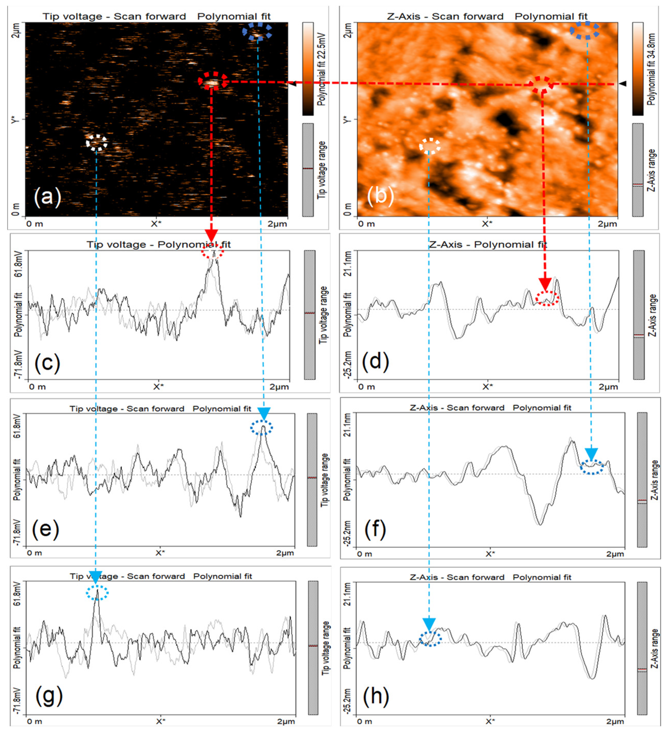
3.3. Atomic and Kevin Probe Force Microscopy
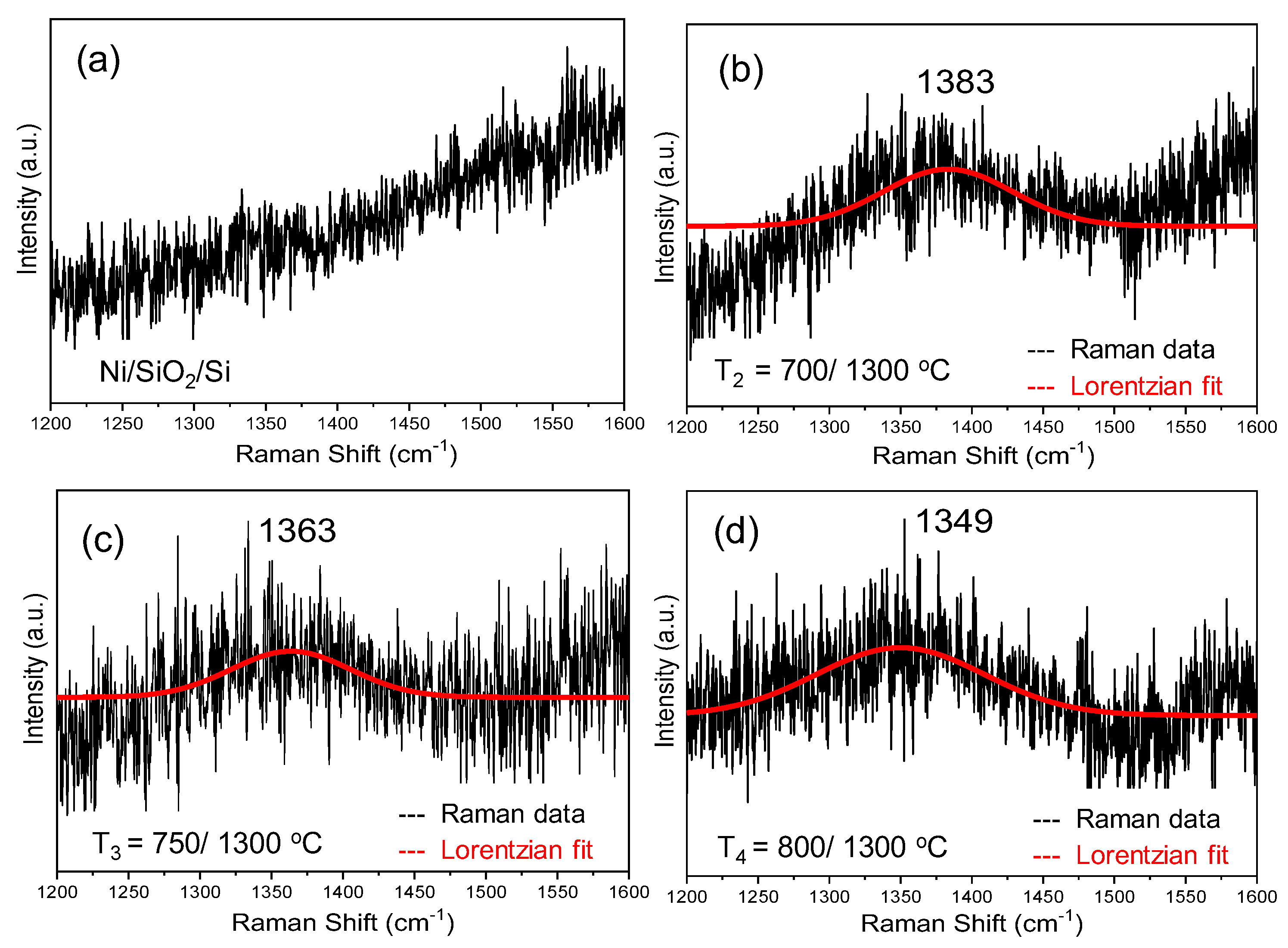
For the observation of h-BN QDs, AFM and KPFM were used to investigate the surface morphology and contact potential distribution as a work function between h-BN nanodots and Ni substrate. Figure 4a shows the KPFM image with a scan area of 2 µm × 2 µm, and Figure 4c,e,g are the line scans of local contact potential difference for sample T2. A random distribution of bright color spots of higher potential voltage, indicating h-BN QDs existence. At the time, the AFM image was obtained at the same region, shown in Figure 4b,d,f,h, the bright area is the top surface of the samples, and the dark area is in the valleys of the samples. In three line-scan measurements of KPFM and AFM, including a single dot, the peaks were at a different position, which also indicates the existence of the h-BN QDs.
For different growth temperatures, the average surface roughness (Ra) of samples T2, T3, and T4 are 4.15, 8.02 and 8.71 nm, as summarized in Table 1. The local contact potential difference between the h-BN QDs and the Ni substrate is 10.56, 9.75 and 9.63 mV, respectively. The surface roughness of Ni film increased with increasing growth temperature. Therefore, the increase in the roughness could come from the formation of h-BN QDs.

3.4. Raman Analysis

Raman spectra are used to characterize the vibration mode of h-BN QDs. The Raman spectrum of the substrate was displayed in Figure 5a, and it has a similar result as the reference [28]. Then, Figure 5b–d show a weak broad peak which indicates the presence of h-BN nanodots [30]. Lorentzian fitting was used for Raman spectra. Raman shift of h-BN for T2, T3, and T4 samples are at 1383, 1363 and 1349 cm−1, respectively. The presence of crystalline h-BN on Ni can be confirmed by the results of Raman spectra.

3.5. Cathodoluminescence Analysis

The excitation of electrons causes the light emission process of materials. The CL emission spectra of h-BN QDs show four intense peaks at 436, 485, 546, and 610 nm for samples T1 and T2 in Figure 6, indicating the defect luminescence of h-BN, such as vacancies and impurities. The peak intensity increased as K-cell temperature increased to 1300 °C, which means the luminescence of h-BN QDs increased. The CL spectrum with peaks at 436 and 485 nm is attributed to the trapping centers in h-BN, as mentioned by Nistor et al. [31]. Furthermore, CL spectra for samples T2 and T4 in Figure 6 revealed a significant increase in the peak intensity when growth temperature increased to 800 °C, indicating the better formation of h-BN QDs. Interestingly, the peak at 436 nm disappeared as the substrate temperature increased. It could be the annealing effect to reduce the defects in h-BN QDs.

4. Conclusions

In summary, the investigation of h-BN quantum dots grown on polycrystalline Ni/SiO2/Si substrates by the PA-MBE was performed. During the growth, RHEED patterns changed significantly from foggy to spotty with bright rings, indicating surface transformation to polycrystalline due to the growth of h-BN quantum dots. The results of KPFM and AFM confirm that h-BN was deposited in the form of nanodots on the substrate. Raman spectrum can perform the presence of crystal h-BN. The results of CL spectra indicated the emission of h-BN quantum dots by the defect state in the crystal. When substrate temperature and K-cell temperature of the boron source were increased, CL spectra increased in intensity and also had a sharp emission peak due to the quantum confinement effect of h-BN quantum dots.

Author Contributions

Conceptualization, I.-S.Y.; resources, I.-S.Y. and S.-H.C.; data curation, W.-C.H. and N.N.; writing—original draft preparation, N.N. and C.-Y.L.; writing—review and editing, I.-S.Y.; All authors have read and agreed to the published version of the manuscript.

Funding

This research was funded by Ministry of Science and Technology, Taiwan, grant number MOST 109-2221-E-259-004- MY3.

Institutional Review Board Statement

Not applicable.

Informed Consent Statement

Not applicable.

Data Availability Statement

Not applicable.

Acknowledgments

The authors acknowledge the Ministry of Science and Technology, Taiwan, for financially supporting this study. All authors would also like to thank Stanley Wu, Micheal Chen, and Huang-Choung Chang of ULVAC Taiwan Inc. for the support and maintaining of our PA-MBE system.

Conflicts of Interest

The authors declare no conflict of interest.

References

  1. Cheng, T.S.; Davies, A.; Summerfield, A.; Cho, Y.; Cebula, I.; Hill, R.J.A.; Mellor, C.J.; Khlobystov, A.N.; Taniguchi, T.; Watanabe, K.; et al. High temperature MBE of graphene on sapphire and hexagonal boron nitride flakes on sapphire. J. Vac. Sci. Technol. B 2016, 34, 02L101. [Google Scholar] [CrossRef] [Green Version]
  2. Lee., S.H.; Jeong, H.; Okello, O.F.N.; Xiao, S.; Moon, S.; Kim, D.Y.; Kim, G.-Y.; Lo, J.-I.; Peng, Y.-C.; Cheng, B.-M.; et al. Improvements in structural and optical properties of wafer-scale hexagonal boron nitride film by post-growth annealing. Sci. Rep. 2019, 9, 10590. [Google Scholar] [CrossRef] [PubMed] [Green Version]
  3. Wofford, J.M.; Nakhaie, S.; Krause, T.; Liu, X.; Ramsteiner, M.; Hanke, M.; Riechert, H.; Lopes, J.M.J. A hybrid MBE-based growth method for large-area synthesis of stacked hexagonal boron nitride/graphene heterostructures. Sci. Rep. 2017, 7, 43644. [Google Scholar] [CrossRef] [Green Version]
  4. Ahmed, K.; Dahal, R.; Weltz, A.; Danon, J.J.Q.; Lu, Y.; Bhat, I.B. Effects of sapphire nitridation and growth temperature on the epitaxial growth of hexagonal boron nitride on sapphire. Mater. Res. Express 2017, 4, 015007. [Google Scholar] [CrossRef] [Green Version]
  5. Watanabe, K.; Taniguchi, T.; Kanda, H. Direct-bandgap properties and evidence for ultraviolet lasing of hexagonal boron nitride single crystal. Nat. Mater. 2004, 3, 404–409. [Google Scholar] [CrossRef]
  6. Chugh, D.; Wong-Leung, J.; Li, J.; Lysevych, M. Flow modulation epitaxy of hexagonal boron nitride. 2D Mater. 2018, 5, 045018. [Google Scholar] [CrossRef]
  7. Wang, H.; Zhang, X.; Liu, H.; Yin, Z.; Meng, J.; Xia, J.; Meng, X.M.; Wu, J.; You, J. Synthesis of large-sized single-crystal hexagonal boron nitride domains on nickel foils by ion beam sputtering deposition. Adv. Mater. 2015, 27, 8109–8115. [Google Scholar] [CrossRef]
  8. Siegel, G.; Gryzbowcki, G.; Hilton, A.; Muratore, C.; Snure, M. Growth of multi-layer hbn on Ni (111) substrates via MOCVD. Crystals 2019, 9, 339. [Google Scholar] [CrossRef] [Green Version]
  9. Nakhaie, S.; Heilmann, M.; Krause, T.; Hanke, M.; Lopes, J.M.J. Nucleation and growth of atomically thin hexagonal boron nitride on Ni/MgO (111) by molecular beam epitaxy. J. Appl. Phys. 2019, 125, 115301. [Google Scholar] [CrossRef]
  10. Tonkikh, A.A.; Voloshina, E.N.; Werner, P.; Blumtritt, H.; Senkovskiy, B. Structural and electronic properties of epitaxial multilayer h -BN on Ni (111) for spintronics applications. Sci. Rep. 2016, 6, 23547. [Google Scholar] [CrossRef] [Green Version]
  11. Khanaki, A.; Xu, Z.; Tian, H.; Zheng, R.; Zuo, Z.; Zheng, J. Self-assembled cubic boron nitride nanodots. Sci. Rep. 2017, 7, 4087. [Google Scholar] [CrossRef] [Green Version]
  12. Tsai, C.L.; Kobayashi, Y.; Akasaka, T.; Kasu, M. Molecular beam epitaxial growth of hexagonal boron nitride on Ni (111) substrate. J. Cryst. Growth 2019, 311, 3054–3057. [Google Scholar] [CrossRef]
  13. Cui, Z.; He, Y.; Tian, H.; Khanaki, A.; Xu, L.; Shi, W.; Liu, J. Study of direct tunneling and dielectric breakdown in molecular beam epitaxial hexagonal boron nitride monolayers using metal–insulator–metal devices. ACS Appl. Electron. Mater. 2020, 2, 747–755. [Google Scholar] [CrossRef]
  14. Nakhaie, S.; Wofford, J.M.; Schumann, T.; Jahn, U.; Ramsteiner, M.; Hanke, M.; Lopes, J.M.J.; Riechert, H. Synthesis of atomically thin hexagonal boron nitride films on nickel foils by molecular beam epitaxy. Appl. Phys. Lett. 2015, 106, 213108. [Google Scholar] [CrossRef] [Green Version]
  15. Cheng, T.S.; Summerfield, A.; Mellor, C.J.; Khlobystov, A.N.; Eaves, L.; Foxon, C.T.; Beton, P.H.; Novikov, S.V. High-temperature molecular beam epitaxy of hexagonal boron nitride with high active nitrogen fluxes. Materials 2018, 11, 1119. [Google Scholar] [CrossRef] [Green Version]
  16. Wrigley, J.; Bradford, J.; James, T.; Cheng, T.S.; Thomas, J.; Mellor, C.J.; Khlobystov, A.N.; Eaves, L.; Foxon, C.T.; Novikov, S.V.; et al. Epitaxy of boron nitride monolayers for graphene-based lateral heterostructures. 2D Mater. 2021, 8, 034001. [Google Scholar] [CrossRef]
  17. Xu, Z.; Khanaki, A.; Tian, H.; Zheng, R.; Suja, M.; Zheng, J.G.; Liu, J. Direct growth of hexagonal boron nitride/graphene heterostructures on cobalt foil substrates by plasma-assisted molecular beam epitaxy. Appl. Phys. Lett. 2016, 109, 043110. [Google Scholar] [CrossRef]
  18. Xu, Z.; Tian, H.; Khanaki, A.; Zheng, R.; Suja, M.; Liu, J. Large-area growth of multi- layer hexagonal boron nitride on polished cobalt foils by plasma-assisted molecular beam epitaxy. Sci. Rep. 2017, 7, 43100. [Google Scholar] [CrossRef]
  19. Vuong, T.Q.P.; Cassabois, G.; Valvin, P.; Rousseau, E.; Summerfield, A.; Mellor, C.J.; Cho, Y.; Cheng, T.S.; Albar, J.D.; Eaves, L.; et al. Deep ultraviolet emission in hexagonal boron nitride grown by high-temperature molecular beam epitaxy. 2D Mater. 2017, 4, 021023. [Google Scholar] [CrossRef]
  20. Page, R.; Casamento, J.; Cho, Y.; Rouvimov, S.; Xing, H.G.; Jena, D. Rotationally aligned hexagonal boron nitride on sapphire by high-temperature molecular beam epitaxy. Phys. Rev. Mater. 2019, 3, 064001. [Google Scholar] [CrossRef] [Green Version]
  21. Bhowmick, S.; Singh, A.K.; Yakobson, B.I. Quantum dots and nanoroads of graphene embedded in hexagonal boron nitride. J. Phys. Chem. C 2011, 115, 9889–9893. [Google Scholar] [CrossRef]
  22. Srivastava, M.; Singh, J.; Kuila, T.; Layek, R.K.; Kim, N.H.; Lee, J.H. Recent advances in graphene and its metal-oxide hybrid nanostructures for lithium-ion batteries. Nanoscale 2015, 7, 4820–4868. [Google Scholar] [CrossRef] [PubMed]
  23. Zhang, Q.; Nie, C.; Chang, C.; Guo, C.; Jin, X.; Qin, Y.; Li, F.; Li, Q. Highly luminescent red emitting CdZnSe/ZnSe quantum dots synthesis and application for quantum dot light emitting diodes. Opt. Mater. Express 2017, 7, 3875. [Google Scholar] [CrossRef]
  24. Fan, Z.; Li, S.; Yuan, F.; Fan, L. Fluorescent graphene quantum dots for biosensing and bioimaging. RSC Adv. 2015, 5, 19773–19789. [Google Scholar] [CrossRef]
  25. Shammas, J.; Sun, T.; Koeck, F.A.M.; Rezykyan, A.; Nemanich, R.J. In situ photoelectron spectroscopic characterization of c-BN films deposited via plasma enhanced chemical vapor deposition employing fluorine chemistry. Diam. Relat. Mater. 2015, 56, 13–22. [Google Scholar] [CrossRef]
  26. Susanto, I.; Kan, K.-Y.; Yu, I.-S. Temperature effects for GaN films grown on 4H-SiC substrate with 4° miscutting orientation by plasma-assisted molecular beam epitaxy. J. Alloys Compd. 2017, 723, 21–29. [Google Scholar] [CrossRef]
  27. Hasegawa, S. Reflection High-Energy Electron Diffraction. In Characterization of Materials; John Wiley & Sons: Hoboken, NJ, USA, 2012; pp. 1928–1931. [Google Scholar]
  28. Laleyan, D.A.; Mengle, K.; Zhao, S.; Wang, Y.; Kioupakis, E.; Mi, Z. Effect of growth temperature on the structural and optical properties of few-layer hexagonal boron nitride by molecular beam epitaxy. Opt. Express 2018, 26, 23031. [Google Scholar] [CrossRef]
  29. Xie, B.; Liu, H.; Hu, R.; Wang, C.; Hao, J.; Wang, K.; Luo, X. Targeting cooling for quantum dots in white QDs-LEDs by hexagonal boron nitride platelets with electrostatic bonding. Adv. Funct. Mater. 2018, 28, 1081407. [Google Scholar] [CrossRef]
  30. Yamada, H.; Inotsume, S.; Kumagai, N.; Yamada, T.; Shimizu, M. Chemical vapor deposition growth of BN thin films using B2H6 and NH3. Phys. Status Solidi B 2020, 257, 1900318. [Google Scholar] [CrossRef]
  31. Nistor, S.V.; Nistor, L.C.; Joita, A.C.; Vlaicu, A.M. Presence and distribution of impurity defects in crystalline cubic boron nitride. A spectroscopic study. Radiat. Meas. 2019, 123, 21–25. [Google Scholar] [CrossRef]
Figure 1. Schematic of the preparation and characterizations of h-BN QDs.
Crystals 12 00347 g001
Figure 2. RHEED patterns: (a) Ni/SiO2/Si substrate after thermal cleaning, (b) T1 (700/1200 °C), (c) T2 (700/1300 °C), and (d) T4 (800/1300 °C).
Crystals 12 00347 g002
Figure 3. FE-SEM images, (a) Ni Substrate, (b) T2 (700/1300 °C), (c) T4 (800/1300 °C), and (d) EDS analysis of T4.
Crystals 12 00347 g003
Figure 4. (a,c,e,g) KPFM images for sample T2; (b,d,f,h) AFM images at the same region of sample T2.
Crystals 12 00347 g004
Figure 5. Raman spectra: (a) Ni/SiO2/Si substrate, (b) T2, (c) T3, and (d) T4 samples.
Crystals 12 00347 g005
Figure 6. Cathodoluminescence spectra: h-BN quantum dots grown at different K-cell temperatures for samples T1 (700/1200 °C) and T2 (700/1300 °C), and at different substrate temperatures for samples T2 (700/1300 °C) and T4. (800/1300 °C).
Crystals 12 00347 g006
Table 1. Surface roughness (Ra, nm) and local contact potential difference (LCPD, mV) of T2, T3, and T4 samples for different growth temperatures.
ParameterT2 (700 °C)T3 (750 °C)T4 (800 °C)
Ra LCPD Ra LCPD Ra LCPD
Average 4.1510.568.029.758.719.63
Max. peak height20.7261.8229.4159.1947.0168.13
Max. peak depth−25.23−64.89−38.63−55.21−58.04−62.85
Publisher’s Note: MDPI stays neutral with regard to jurisdictional claims in published maps and institutional affiliations.

