1. Introduction
Graphene, a two-dimensional material composed of a single atomic layer of carbon, was discovered in 2004 and has attracted much attention [
1]. Benefiting from its atomic thin film layer and extremely high carrier mobility, graphene is considered to be one of the most promising candidates for extending Moore’s law in future nanoelectronics. For example, a graphene field effect transistor (GFET) with high cut-off frequency (407 GHz) and maximum oscillation frequency (200 GHz) has been fabricated [
2,
3]. In addition, a graphene frequency multiplier and a monolithic integrated receiver on eight-inch wafers have also been reported [
4,
5]. In GFET, the conductance between source and drain is modulated by a gate. Hence, the gate insulator is quite crucial in determining the performance of the GFET. In order to improve the performance and integrated density of the integrated circuits based on graphene, the channel length should be scaled down. To maintain strong gate control on conduction channel during the dimension scaling down, an increasingly thinner gate oxide is required for improving the drain–current response of the transistor to the applied gate voltage, and to avoid the short channel effect [
6]. As a result, the deposition of an ultrathin, high-k gate dielectric layer with nanoscale thickness, and few pin holes on the graphene is necessary [
7].
In conventional silicon processes, the dielectric layer of transistors with top-gate structures is often deposited by evaporation, sputtering, and chemical vapor deposition. Unfortunately, the above methods may not be suitable for the gate dielectric deposition of GFET. This can be attributed to two reasons. One is that the regular deposition processes discussed above usually cause difficulty in obtaining a dielectric layer with the required precision and thickness. The other reason is that the deposition process may introduce great damage to the graphene film. Therefore, it is an urgent requirement to deposit high-quality gate dielectric films on the graphene surface without significantly damaging the graphene structure or deteriorating the graphene properties.
Atomic layer deposition (ALD) is an important technique for depositing ultrathin dielectric films. The sample was exposed to a mixed gas reaction atmosphere. The kind of reaction gases, grown temperature, and grown cycles can be precisely controlled. Due to the self-limiting reaction of the chemical source on the material surface, the ALD process enables precise thickness control and excellent uniformity of the dielectric film over large areas [
8]. Compared with other processes, the ALD process usually works at lower temperatures and therefore does not tend to introduce additional defects on the graphene. Due to these advantages, ALD is the best choice for depositing dielectric layers on graphene surfaces.
However, there are still some challenges for the atomic layer deposition of high-k film on a graphene surface. For example, the surface of graphene is chemically inert and hydrophobic. Therefore, the graphene lacks dangling bonds, which are necessary for the atomic layer deposition process. The high-k dielectric film is difficult to nucleate on graphene through the direct ALD deposition process. Previous reports have illustrated that the quality of the deposited film strongly depends on the synthesis method of graphene. In the case of the exfoliated graphene, the direct ALD deposition process will lead to a nonuniform coverage of the film on the graphene. The region at the step edge is usually preferentially covered [
9]. The coverage of the ALD dielectric film on graphene grown by chemical vapor deposition (CVD) shows a significant increase due to some dangling bonds induced by defects and wrinkles during transfer. However, the dielectric film is still discontinuous [
10]. To overcome this issue, various surface preparation techniques have been proposed. Lin et al. [
11] used NO
2 to functionalize graphene. The functional layer introduces a large number of dangling bonds on the graphene surface and leads to a uniform ALD dielectric film. However, the breakage of C-C bonds during the NO
2 function process will result in a significant degeneration of carrier mobility for graphene [
12]. Zhang et al. [
13] also obtained uniform Al
2O
3 films on the graphene surface through controlling the growth temperature and choosing a suitable purging time in the ALD process. However, the overdependence on the experimental conditions could significantly affect the reproducibility of the experiments due to the extreme sensitivity of 2D materials to environmental changes. Cao et al. [
14] and Zheng et al. [
15] achieved uniform ALD dielectric films on the graphene surface by utilizing the pre-water treatment. In this method, four cycles of pre-water treatment provided uniform nucleation sites for ALD, resulting in uniform Al
2O
3 films with a dielectric constant of 7.2 and a breakdown critical electrical field of 9 MV/cm. However, the bonding of the CVD graphene and substrate was poor, and the pre-water treatment can lead to graphene detachment from the substrate. Meanwhile, there are few related studies, and the stability of the conditions needs to be further explored [
16]. In addition, various kinds of polymers have been used as ALD seed layers, such as NFC [
7], PTCDA [
17], and BCB [
18]. However, the polymer layers tend to be thicker and have lower dielectric constants, which can significantly reduce the gate capacitance and control capability. Moreover, the polymer layers may introduce unintentional doping in graphene. Recently, the metal oxide seed layer has been introduced into the fabricating process of top-gated GFETs for ALD dielectric deposition [
19]. The thin nucleation layer of oxidized Al was deposited on the graphene before the ALD process. Using this method, the dielectric grown by the ALD process can have few pinholes. However, due to the high surface mobility of aluminum atoms on graphene, the Al metal deposited by e-beam evaporation tends to aggregate and form clusters. In order to cover the entire graphene surface, high critical thickness of the aluminum seed layer is needed [
20]. Due to the oxidation ratio of the Al metal greater than 1, the actual thickness of an Al
2O
3 film formed by the Al natural oxidation process will be expanded [
21]. In addition, the incompletely oxidized seed layer may introduce some charged impurities, which enhance the electron scattering at the graphene surface. These factors lead to the degeneration of the device performance.
In this paper, the high-k dielectric deposition method in GFET using alumina residual as a seed layer was proposed. Firstly, the Al metal film was deposited on the surface of the graphene. After the Al was naturally oxidized, it was removed by ammonia. Subsequently, the ultrathin Al2O3 film was deposited by ALD and the continuous ultrathin dielectric film was thus formed. The surface morphology of graphene samples before and after the atomic layer deposition was observed by scanning electron microscopy (SEM) and atomic force microscopy (AFM). Raman analysis showed that the treatment process would not introduce additional defects in the graphene. Finally, top-gate graphene transistors using the regular process and the improved process were fabricated. The electrical properties of the devices were measured at room temperature using the Keithley 4200 semiconductor parameter analyzer. The gate transconductance (gm)of our GFET was increased by 44.7% compared with that using the regular dielectric deposition method, in which a metal oxide film was used as a seed layer. The increasing gm indicates improved gate control capability of our GFET.
3. Results and Discussion
Figure 1 presents the SEM image of the surface of Al
2O
3 deposited on the graphene without a seed layer. The Al
2O
3 film is patchy and discontinuous on the chemically inert graphene, which can be contributed to the lack of dangling bonds in the completed lattice area. For the CVD graphene, wrinkles and defects were introduced by the growing and transfer process. The dangling bonds, originating from the wrinkles and defects, provided the nucleation for the ALD deposition. The Al
2O
3 film with large pinholes is not suitable for subsequent top-gate GFET fabrication.
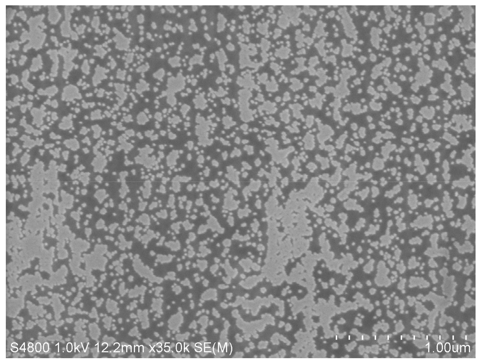
In this paper, the alumina residual layer, originating from the removed naturally oxidized Al film, was the seed layer for the ALD process. The Al films with different thicknesses of 2 nm, 5 nm, and 10 nm were first grown on the graphene surface, and then exposed in air to form self-oxidized Al
2O
3. The surface morphologies were analyzed by SEM and AFM, respectively (seen in
Figure 2a–c). Owing to the high mobility, the aluminum atoms on the graphene surface tend to form island clusters. Hence, a large number of pinholes and cracks were observed in the seed layer, which was formed by a 2 nm Al film on graphene. However, the coverage of the seed layer can be improved as the thickness of the Al film increases. Such improvement is even more notable on the 10 nm seed layer, as shown in
Figure 2c. The root mean square (RMS) roughness values of the 2 nm, 5 nm, and 10 nm seed layer surfaces were measured by AFM, which were 1.192 nm, 1.108 nm, and 1.61 nm, respectively. The lowest roughness was found on the 5 nm seed layer surface, which can be attributed to the effect of increased alumina coverage being greater than the effect of the increased crack depth. As the thickness of the seed layer increased, the size of the alumina clusters also gradually increased, which meant that the surface of the seed layer presented the highest roughness at 10 nm. The 10 nm Al
2O
3 film was further deposited on each seed layer by the ALD process. The surface morphologies of the final dielectric films are shown in
Figure 2d–f. It can be found in
Figure 2d that, for the 2 nm seed layer, the obtained dielectric is inhomogeneous, and a large number of pinholes can be observed on the film surface. However, it can be seen from
Figure 2e,f that closed dielectric films can be obtained on the seed layers of 5 nm and 10 nm, which is mainly attributed to the increased coverage of the seed layer. Therefore, the fabrication of graphene transistors requires aluminum films at least 5 nm thick as seed layers for the standard Al evaporation methods.
Figure 3 shows the Raman spectra of pristine graphene (black line) as well as the graphene after deposition of 2 nm (red line), 5 nm (green line), and 10 nm (blue line) Al films bye-beam evaporation and natural oxidation to Al
2O
3 seed layers in air, respectively. The baselines of the pristine graphene and the graphene with a 2 nm alumina seed layer are relatively flat over the entire range of measurements. In contrast, the graphene with 5 nm and 10 nm alumina seed layers show significant background signals, indicating the presence of incompletely oxidized aluminum metal in the 5 nm and 10 nm seed layers. The incompletely oxidized aluminum particles could generally introduce strong electron scattering in graphene and lead to the deterioration of carrier mobility.
As mentioned previously, the Al
2O
3 seed layer limits the minimal possible thickness of dielectrics and may also introduce extra scattering centers. In order to avoid this adverse effect, we attempt to remove the Al
2O
3 seed layer from the graphene surface using an etching solution. The alumina residual provides the nucleation sites for the following ALD process. Solution A (1 partH
3PO
4:10 part DI water) and solution B (1 part 36% NH
4OH:10 part DI water) were used as etching solutions, respectively. Generally, alumina does not react with ammonia, but the ultrathin Al
2O
3 films can be etched by ammonia solution.
Figure 4a shows the graphene surface of 2 nm self-oxidized Al
2O
3 seed layer etched by solution A at room temperature for 5 min.
Figure 4b–d show the 2 nm, 5 nm, and 10 nm self-oxidized Al
2O
3 seed layers, etched by solution B at the same conditions. It can be clearly seen that the Al
2O
3 film can be removed by both solution A and solution B. The residues of which would be retained on the graphene surface previously covered by Al
2O
3. The residues of the self-oxidized Al
2O
3 films can provide the necessary nucleation sites for subsequent ALD process. The surface morphologies of the residue-seeded Al
2O
3, treated by solution A and solution B, are shown in
Figure 4e,f. It can be seen that the Al
2O
3 film, deposited on the seed layer, treated by solution B, exhibited higher quality with fewer pinholes compared with that treated by solution A. This may be attributed to the following reason. Because of the more active reaction between alumina and H
3PO
4 compared with that between ammonia and H
3PO
4, less residue will be left on the surface of the graphene after the etching process with solution A than solution B. The inadequate enucleation sites meant that the ALD Al
2O
3 film deposition was of poor quality. The effect of the removed seed layer thickness on the Al
2O
3 dielectric layer was further investigated. The graphene samples covered with 5 nm and 10 nm Al
2O
3 seed layers were etched by solution B. Then, the 10 nm ALD Al
2O
3 layer was deposited on the graphene.
Figure 4f–h show the SEM images of the surface morphology of the Al
2O
3 dielectric layers for different thickness seed layers etched by solution B. The number of pinholes decreases as the thickness of the removed seed layer increases. The residues left after the removal of the 10 nm self-oxidized alumina seed layer can provide enough nucleation sites for the subsequent ALD process and lead to a good uniformity of Al
2O
3 film. However, the number of particles that are not completely removed also increases with the thickness of the seed layer, which may lead to an increased roughness of the dielectric film.
Raman spectra further confirmed that no extra defects were generated in the graphene with the seed layer etching process.
Figure 5 shows the Raman spectra of graphene for different process steps during the deposition of the dielectric film. For the pristine graphene transferred to the SiO
2/Si substrate, the G and 2D peaks in the Raman spectra are located at 1587 cm
−1 and 2708 cm
−1, respectively. Usually, the G and 2D peaks of graphene are at 1580 cm
−1 and 2700 cm
−1, respectively. However, the blueshifts of the G peak and the 2D peak of graphene were observed in our sample. The blue shift of the Raman peak indicates increased phonon energy in graphene, which can be attributed to the doping effect originating from the absorption of water in the air during the transfer process [
22,
23,
24,
25,
26]. In addition, the intensity ratio of the 2D peak to the G peak (I
2D/I
G) in the Raman spectra is estimated to be 2.13, which indicates that the graphene in the experiment is a single layer. It can be seen from the figure that a D peak also appears near the position of 1370 cm
−1, indicating the presence of point defects or structural disorders in the graphene. The disorders may originate from the wrinkles generated during the transfer process [
27]. After the graphene surface was covered by the 2 nm Al
2O
3 film, deposited by electron beam evaporation, the intensity of all peaks in the Raman spectra became weaker. The 2D peak shifted left, to the position of 2705 cm
−1.The redshift of the 2D peak may be due to the electron doping of graphene caused byAl
2O
3 film. The extra electrons mainly originate from the negative charge induced in graphene by Al
3+ in alumina. After the etching of 2 nm Al
2O
3 by solution B, the position of the 2D peak in the corresponding Raman spectra shifted right to 2706 cm
−1, but it was still lower than 2708 cm
−1 in the original graphene. The result suggests that some residues of Al
2O
3 still existed on the graphene surface. It should be noted that the intensity ratio of the D-peak to the G-peak (I
D/I
G) in the Raman spectra of graphene did not change significantly before and after the etching process, which indicates that the graphene was not damaged and reserved its original properties. The subsequent ALD deposition made the position of the 2D peak shift slightly left again, to 2705 cm
−1.
The top-gated graphene field effect transistor was further fabricated using our improved high-k dielectric deposition method. First, the active region of graphene was etched by oxygen plasma to isolate the device. Then, the source and drain electrodes were defined using regular lithography followed by e-beam evaporation of Ti/Au (20/200 nm) metal contacts, and the lift-off process. Subsequently, a 10 nm Al film was deposited on the graphene surface by electron-beam evaporation and naturally oxidized in air to form Al
2O
3, which was then removed by solution B. An additional Al
2O
3 film (10 nm) was grown as the top-gate dielectric by ALD. Finally, the Ti/Au (20/200 nm) top-gate electrode was fabricated. We also prepared the graphene transistor using the regular process with the seed layer of 5 nm and an additional Al
2O
3 film of 10 nm.
Figure 6a,b show optical images of top-gate graphene transistors fabricated using the improved process and the regular process, respectively. The gate length and gate width of GFET were 2.5 μm and 40 μm, respectively.
The electrical characteristics of both graphene transistors were measured by the Keithley 4200 semiconductor parameter analyzer at room temperature.
Figure 6c shows the output characteristics of top-gate graphene transistors fabricated by the improved (blue line) and regular (red line) processes, respectively. The drain voltage (
VDS) scanned from 0 V to 1 V. The top-gate voltage (
VG) swept from −2 V to 2 V. It can be observed that the drain currents of both devices showed almost linear correlation with the drain voltages, and no current saturation occurred in the measured ranges. The linear relationship between
IDS and
VDS was attributed to the zero-gap band structure of the graphene. However, in some cases, due to the presence of both carriers in the graphene channel, the drain current will first enter saturation, and then enter the secondary linear region, which is known as the “kink” effect [
28]. When the drain voltage is kept constant, the drain current of both devices decreases as the gate voltage increases. This is because when the gate voltage is in the range of −2V to 2V, the graphene transistor works in the branch of the hole conducting, and the number of hole carriers decreases gradually with the increase gate voltage. Under the same conditions, the drain current of the improved device was significantly larger than that of the regular device. The increasing drain current of the GFET fabricated by improved dielectric deposition method can be attributed to the enhanced gate control capability induced by the thinner dielectric film. Benefiting from the enhanced gate control capability, the number of carriers in the graphene channel increased.
Figure 6d shows the transfer characteristics of top-gate graphene transistors prepared using the improved (blue line) and regular (red line) processes at different drain biases of 1.5 V, 1.75 V, and 2 V. Generally, the transfer characteristic curve of a standard GFET presents a “V” shape. The conductance of GFET in the positive direction of the curve is controlled by electrons, while that in the negative direction of the curve is controlled by holes [
29]. However, our GFET only showed the hole branch in the measurement range. This indicates that our GFET was p-type doped, which can be attributed to the photoresist residue and water adsorption on graphene.
The transconductance (
gm) specifies the current response of the transistor to a small modulation of the gate voltage. It is a key parameter for the radio frequency performance of GFETs. The
gm can be calculated as the derivative of
IDS with respect to
VG (
gm =
dIDS/
dVG). The inset of
Figure 6d shows the variation of the transconductance as a function of gate voltage for the improved GFET (blue line) and regular GFET (red line) at different drain biases of 1.5 V, 1.75 V, and 2 V. Respectively, the peak values of
gm in the regular GFET were 1.57 mS, 1.68 mS, and 1.77 mS, while that of improved device were 2.18 mS, 2.43 mS, and 2.68 mS, with an average enhancement of 44.7%, showing the apparent improvement by adopting this new dielectric deposition method. In addition, the field effect carrier mobility of a GFET(
μ) can be estimated through
μ =
gmL/
VDSWCOX [
29,
30,
31]. The
L is the gate length,
W is the total gate width, and
COX is the capacitance per unit area of the oxide layer. The dielectric constant of alumina is determined as 7.9 (seen in the
Supplementary Materials [
19,
32]). Considering the dielectric layer thicknesses of 10 nm and 15 nm for the improved and regular devices, respectively, their capacitances per unit area of oxide layer can be obtained as 7 × 10
−3 F/m
2 and 4.67 × 10
−3 F/m
2, respectively. The hole mobility of both devices can be calculated as 119.6 cm
2/Vs and 118.4 cm
2/Vs at
VDS = 2 V, which are approximately equal. This suggests that the improved process of growing ALD dielectric layer using Al
2O
3 residues proposed in this paper does not lead to the degradation of graphene carrier mobility. Top-gate leakage currents were also measured in both devices.
Figure 6e shows the top-gate leakage current (
IGS) as a function of
VTG for the improved device and the regular device at different
VDS of 1.5 V, 1.75 V, and 2 V. It can be seen that the
IGS of both devices was only several nA in the measurement range from −1.5 V to 1.5 V, and even though the gate dielectric thickness of the improved device was 5 nm less than that of the regular device, its insulation did not deteriorate significantly within the range of error. These indicate a good quality of the top-gate dielectric Al
2O
3 film fabricated by our new dielectric deposition method.


