
Graphene-Integrated Plasmonic Metamaterial for Manipulation of Multi-Band Absorption, Based on Near-Field Coupled Resonators


 ,
, 
Abstract
:1. Introduction
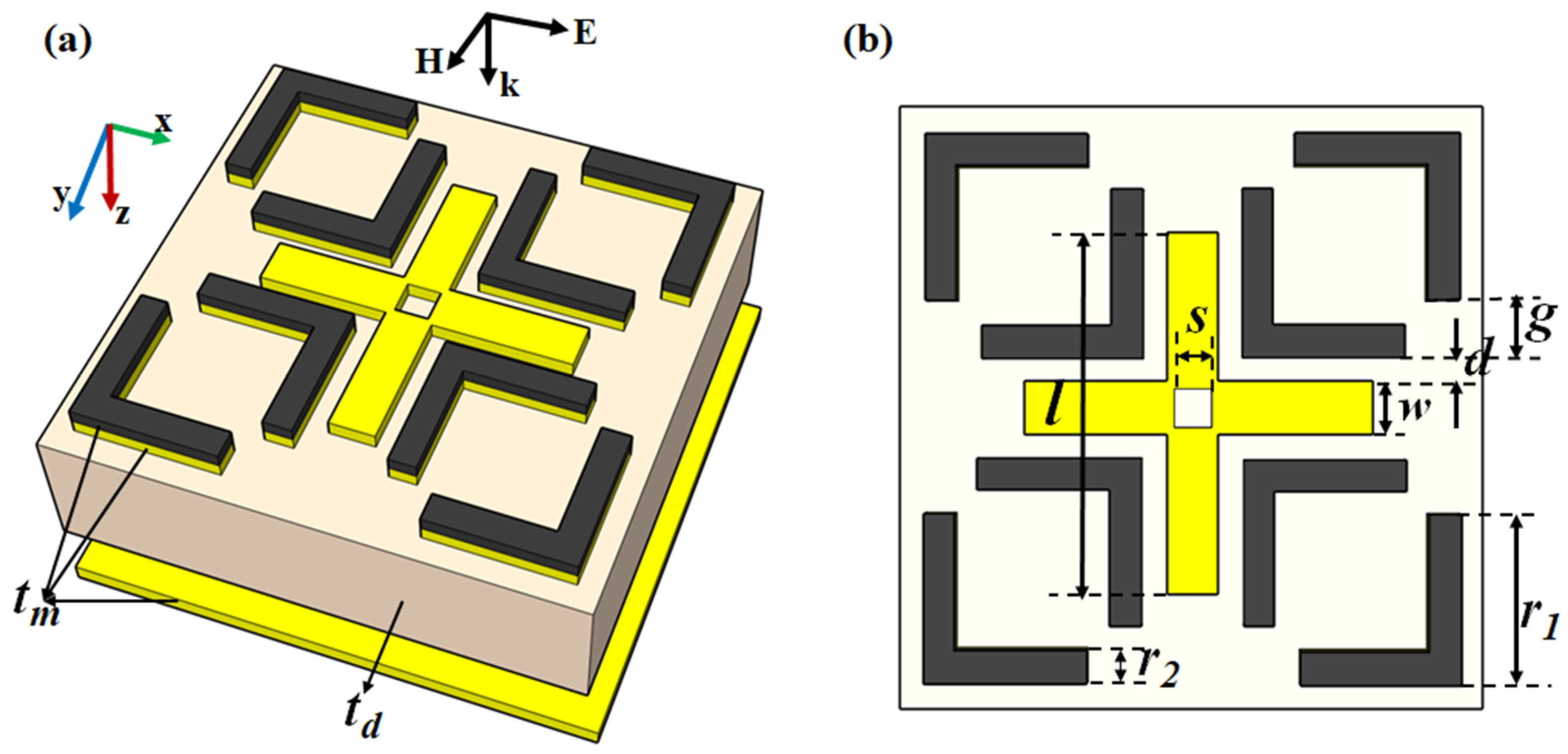
2. Methods
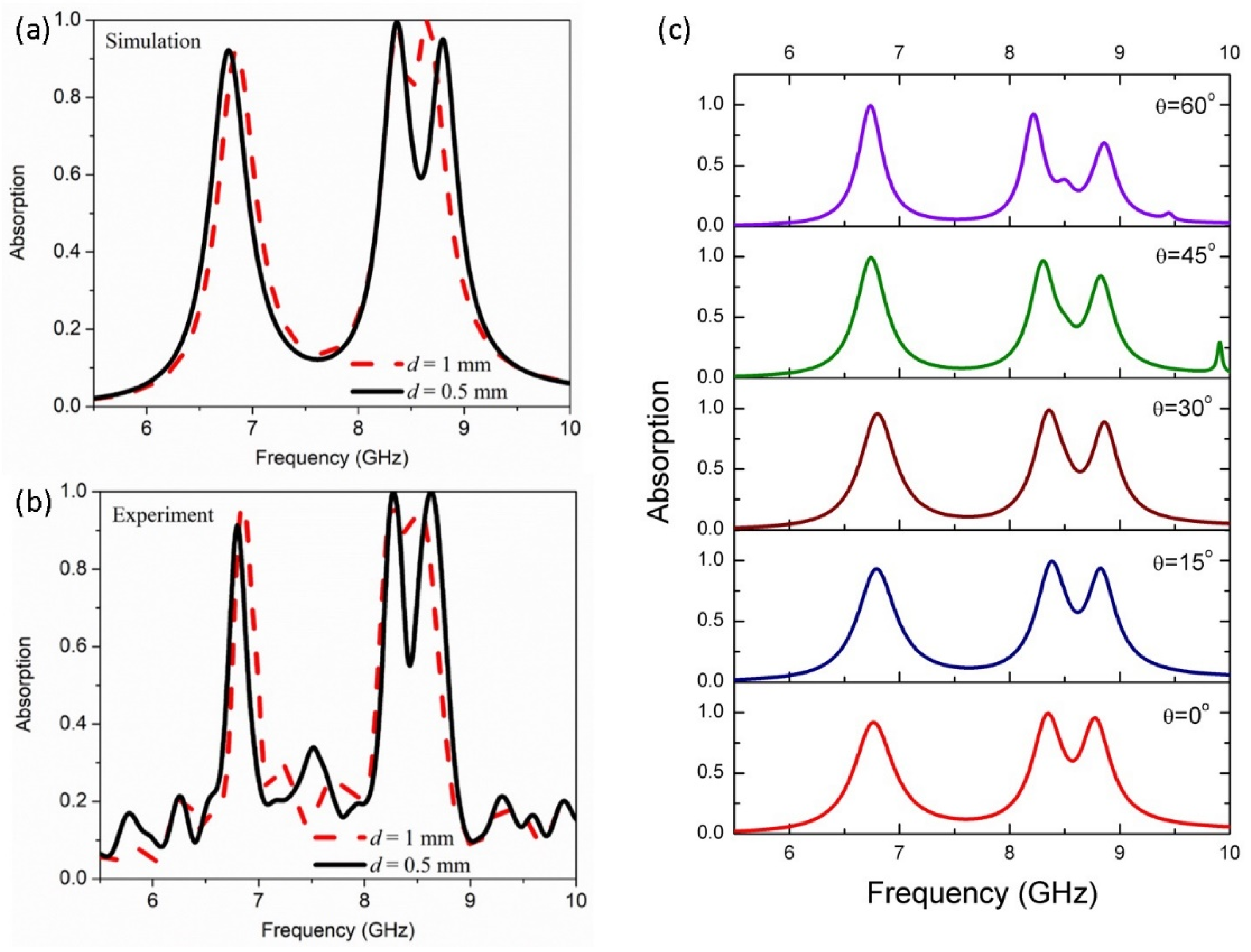
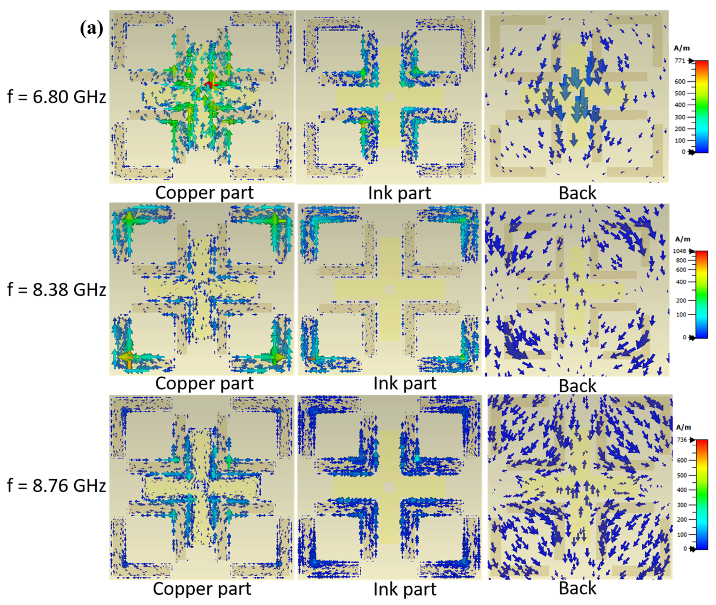
3. Results and Discussion
4. Conclusions
Author Contributions
Funding
Institutional Review Board Statement
Informed Consent Statement
Data Availability Statement
Conflicts of Interest
References
- Ziolkowski, R.W. Pulsed and CW Gaussian beam interactions with double negative metamaterial slabs. Opt. Express 2003, 11, 662–681. [Google Scholar] [CrossRef] [PubMed]
- Veselago, V.G. The Electrodynamics of Substances with Simultaneously Negative Values of ϵ and μ. Sov. Phys. Usp. 1968, 10, 509–514. [Google Scholar] [CrossRef]
- Wang, J.; Allein, F.; Boechler, N.; Friend, J.; Vazquez-Mena, O. Design and fabrication of negative-refractive-index metamaterial unit cells for near-megahertz enhanced acoustic transmission in biomedical ultrasound applications. Phys. Rev. Appl. 2021, 15, 024025. [Google Scholar] [CrossRef]
- Landy, N.I.; Sajuyigbe, S.; Mock, J.J.; Smith, D.R.; Padilla, W.J. Perfect metamaterial absorber. Phys. Rev. Lett. 2008, 100, 207402. [Google Scholar] [CrossRef]
- Norouzi-Razani, A.; Rezaei, P. Broadband polarization insensitive and tunable terahertz metamaterial perfect absorber based on the graphene disk and square ribbon. Results Phys. 2022, 34, 105313. [Google Scholar] [CrossRef]
- Cong, L.; Tan, S.; Yahiaoui, R.; Yan, F.; Zhang, W.; Singh, R. Experimental demonstration of ultrasensitive sensing with terahertz metamaterial absorbers: A comparison with the metasurfaces. Appl. Phys. Lett. 2015, 106, 031107. [Google Scholar] [CrossRef]
- Bui, T.S.; Dao, T.D.; Dang, L.H.; Vu, L.D.; Ohi, A.; Nabatame, T.; Lee, Y.P.; Nagao, T.; Hoang, C.V. Metamaterial-enhanced vibrational absorption spectroscopy for the detection of protein molecules. Sci. Rep. 2016, 6, 32123. [Google Scholar] [CrossRef]
- Cao, Y.; Ruan, C.; Chen, K.; Zhang, X. Research on a high-sensitivity asymmetric metamaterial structure and its application as microwave sensor. Sci. Rep. 2022, 12, 1255. [Google Scholar] [CrossRef]
- Zhang, X.; Liu, Z. Superlenses to overcome the diffraction limit. Nat. Mater. 2008, 7, 435–441. [Google Scholar] [CrossRef]
- Dhama, R.; Yan, B.; Palego, C.; Wang, Z. Super-Resolution Imaging by Dielectric Superlenses: TiO2 Metamaterial Superlens versus BaTiO3 Superlens. Photonics 2021, 8, 222. [Google Scholar] [CrossRef]
- Nagarajan, A.; Erve, K.V.; Gerini, G. Ultra-narrowband polarization insensitive transmission filter using a coupled dielectric-metal metasurface. Opt. Express 2020, 28, 773–787. [Google Scholar] [CrossRef] [PubMed] [Green Version]
- Shan, S.; Wen, F.; Cheng, L. Purified nonlinear guided waves through a metamaterial filter for inspection of material microstructural changes. Smart Mater. Struct. 2021, 30, 095017. [Google Scholar] [CrossRef]
- Dietlein, C.; Luukanen, A.; Popovic, Z.; Grossman, E. A W-band polarization converter and isolator. IEEE Trans. Antennas Propag. 2007, 55, 1804–1809. [Google Scholar] [CrossRef]
- Olan-Nuñez, K.N.; Murphy-Arteaga, R.S. A novel metamaterial-based antenna for on-chip applications for the 72.5–81 GHz frequency range. Sci. Rep. 2022, 12, 1699. [Google Scholar] [CrossRef] [PubMed]
- Wu, T.; Li, W.; Chen, S.; Guan, J. Wideband frequency tunable metamaterial absorber by splicing multiple tuning ranges. Results Phys. 2021, 20, 103753. [Google Scholar] [CrossRef]
- Tennant, A.; Chambers, B. A single-layer tuneable microwave absorber using an active FSS. IEEE Microw. Wirel. Compon. Lett. 2004, 14, 46–47. [Google Scholar] [CrossRef] [Green Version]
- Xu, W.; Sonkusale, S. Microwave diode switchable metamaterial reflector/absorber. Appl. Phys. Lett. 2013, 103, 031902. [Google Scholar] [CrossRef]
- Ling, K.; Yoo, M.; Su, W.; Kim, K.; Cook, B.; Tentzeris, M.M.; Lim, S. Microfluidic tunable inkjet-printed metamaterial absorber on paper. Opt. Express 2015, 23, 110. [Google Scholar] [CrossRef]
- Bilgin, H.; Zahertar, S.; Sadeghzadeh, S.; Yalcinkaya, A.D.; Torun, H. A MEMS-based terahertz detector with metamaterial-based absorber and optical interferometric readout. Sens. Actuator A Phys. 2016, 244, 292–298. [Google Scholar] [CrossRef]
- Li, T.Y.; Wang, L.; Wang, J.M.; Li, S.; He, X.J. A dual band polarization-insensitive tunable absorber based on terahertz MEMS metamaterial. Integr. Ferroelectr. 2014, 151, 157–163. [Google Scholar] [CrossRef]
- Kakenov, N.; Balci, O.; Takan, T.; Ozkan, V.A.; Altan, H.; Kocabas, C. Observation of gate-tunable coherent perfect absorption of terahertz radiation in graphene. ACS Photonics 2016, 3, 1531–1535. [Google Scholar] [CrossRef] [Green Version]
- Liu, M.; Cheng, W.; Zhang, Y.; Zhang, H.; Zhang, Y.; Li, D. Multi-controlled broadband terahertz absorber engineered with VO 2-integrated borophene metamaterials. Opt. Mater. Express 2021, 11, 2627–2638. [Google Scholar] [CrossRef]
- Qi, L.; Liu, C. Broadband multilayer graphene metamaterial absorbers. Opt. Mater. Express 2019, 9, 1298–1309. [Google Scholar] [CrossRef]
- Long, L.V.; Khiem, N.S.; Tung, B.S.; Tung, N.T.; Giang, T.T.; Son, P.T.; Khuyen, B.X.; Lam, V.D.; Chen, L.; Zheng, H.; et al. Flexible Broadband Metamaterial Perfect Absorber Based on Graphene-Conductive Inks. Photonics 2021, 8, 440. [Google Scholar] [CrossRef]
- Pan, K.; Leng, T.; Song, J.; Ji, C.; Zhang, J.; Li, J.; Hu, Z. Controlled reduction of graphene oxide laminate and its applications for ultra-wideband microwave absorption. Carbon 2020, 160, 307–316. [Google Scholar] [CrossRef]
- CST Microwave Studio 2015, License ID: 52856-1. Dassault Systèmes. Available online: http://www.cst.com (accessed on 28 February 2022).
- Weiland, T. A discretization model for the solution of Maxwell’s equations for six-component fields. Arch. Elektron. Übertrag. 1977, 31, 116–120. [Google Scholar]
- Bai, R.; Zhang, C.; Gu, X.; Jin, X.R. Unidirectional reflectionlessness and perfect nonreciprocal absorption in stacked asymmetric metamaterial based on near-field coupling. Appl. Phys. Express 2017, 10, 112001. [Google Scholar] [CrossRef]
- Pham, T.L.; Dinh, H.T.; Le, D.H.; Bui, X.K.; Bui, S.T.; Dang, H.L.; Phan, A.D.; Le, D.T.; Vu, D.L. Dual-band isotropic metamaterial absorber based on near-field interaction in the Ku band. Curr. Appl. Phys. 2020, 20, 331–336. [Google Scholar] [CrossRef]
- Tung, B.S.; Khuyen, B.X.; Kim, Y.J.; Lam, V.D.; Kim, K.W.; Lee, Y.P. Polarization-independent, wide-incident-angle and dual-band perfect absorption, based on near-field coupling in a symmetric metamaterial. Sci. Rep. 2017, 7, 11507. [Google Scholar] [CrossRef] [Green Version]
- Tung, B.S.; Khuyen, B.X.; Kim, Y.J.; Hwang, J.S.; Lam, V.D.; Chen, L.-Y.; Lee, Y.P. Manipulation of the near-field coupling in metamaterial for multi-band absorber. Waves Random Complex Media 2021, 31, 2290–2300. [Google Scholar] [CrossRef]


| Parameter | a | d | g | l | r1 | r2 | s | td | tm | w |
|---|---|---|---|---|---|---|---|---|---|---|
| Value (mm) | 22 | 1 | 1.5 | 11 | 7 | 1 | 0.5 | 1.6 | 0.035 | 2 |
Publisher’s Note: MDPI stays neutral with regard to jurisdictional claims in published maps and institutional affiliations. |
© 2022 by the authors. Licensee MDPI, Basel, Switzerland. This article is an open access article distributed under the terms and conditions of the Creative Commons Attribution (CC BY) license (https://creativecommons.org/licenses/by/4.0/).
Share and Cite
Nam, M.H.; Tung, B.S.; Khuyen, B.X.; Ha, D.T.; Ngoc, N.V.; Tran, M.C.; Le, D.T.; Lam, V.D.; Chen, L.; Zheng, H.; et al. Graphene-Integrated Plasmonic Metamaterial for Manipulation of Multi-Band Absorption, Based on Near-Field Coupled Resonators. Crystals 2022, 12, 525. https://doi.org/10.3390/cryst12040525
Nam MH, Tung BS, Khuyen BX, Ha DT, Ngoc NV, Tran MC, Le DT, Lam VD, Chen L, Zheng H, et al. Graphene-Integrated Plasmonic Metamaterial for Manipulation of Multi-Band Absorption, Based on Near-Field Coupled Resonators. Crystals. 2022; 12(4):525. https://doi.org/10.3390/cryst12040525
Chicago/Turabian StyleNam, Man Hoai, Bui Son Tung, Bui Xuan Khuyen, Duong Thi Ha, Nguyen Van Ngoc, Manh Cuong Tran, Dac Tuyen Le, Vu Dinh Lam, Liangyao Chen, Haiyu Zheng, and et al. 2022. "Graphene-Integrated Plasmonic Metamaterial for Manipulation of Multi-Band Absorption, Based on Near-Field Coupled Resonators" Crystals 12, no. 4: 525. https://doi.org/10.3390/cryst12040525