Article

Photo-Elastic Enhanced Optomechanic One Dimensional Phoxonic Fishbone Nanobeam

1
Institute of Photonics, National Changhua University of Education, Changhua 50007, Taiwan
2
Institute of Imaging and Biomedical Photonics, College of Photonics, National Yang Ming Chiao Tung University, Tainan 71150, Taiwan
*
Author to whom correspondence should be addressed.
Crystals 2022, 12(7), 890; https://doi.org/10.3390/cryst12070890
Submission received: 30 May 2022 / Revised: 20 June 2022 / Accepted: 22 June 2022 / Published: 23 June 2022
(This article belongs to the Special Issue Advances in Phononic Crystals and Elastic Metamaterials)

Abstract

:
We investigated the strength of acousto-optical (AO) interaction in one-dimensional fishbone silicon nanobeam computationally. The structure can generate phononic and photonic band gaps simultaneously. We use defect cavity optical mode and slow light mode to interact with acoustic defect modes. The AO coupling rates are obtained by adding the optical frequency shifts, which result from photo-elastic effect and moving-boundary effect disturbances. The AO coupling rates are strongly dependent on the overlap of acoustic and optical mode distribution. The strength of AO interaction can be enhanced by choosing certain acoustic defect modes that are formed by the stretching of wings and that overlap significantly with optical fields.

1. Introduction

In the past decades, metamaterials have been extensively used in several kinds of devices in quantum computations [1,2]. The spatial distributions of physical parameters in these artificial materials give them the ability to produce entanglement of quantum states [3,4]. These structures with the capability of manipulating electromagnetic waves and acoustic waves by building periodic dispersion relations and forming forbidden frequency band gaps are called photonic crystals (PtC) and phononic crystals (PnC) respectively. When optical or acoustic waves incident to a PtC or PnC, respectively, and the wave frequencies fall within the forbidden band gap, they cannot penetrate into the periodic structure. Based on the features of forbidden band gaps, optical cavities and acoustic cavities can be formed by introducing spatial defects in PtC or PnC and producing high-quality factors [5,6,7,8,9]. As early as 2009, Eichenfield M. et al. [10] demonstrated that 1D PtC nanobeam can also be used to control mechanical vibrations (phonon), which showed the potential in optomechanical interactions. With the inspiration of optomechanical crystals, phoxonic crystals (PxC), which combine both capabilities of the PtCs and PnCs have attracted considerable attention in recent years. Designed PxCs can exhibit optical band gaps and acoustic band gaps in one structure to simultaneously control optical waves and acoustic waves [11,12,13,14,15,16,17,18,19,20]. Thus, PxCs have become an advanced structure for acousto-optic (AO) interaction studies [21,22,23,24,25,26].
AO interaction devices are commonly used for sensing or information translating. For example, Andrews et al. use a coated silicon nitride membrane as a microwave signal transducer and convert the signal between microwaves and optical waves by a Fabry–Pérot cavity [27]. In the quantum regions, Stannigel et al. [28] have given an idea of long-distance quantum communication by using an AO transducer. The qubit information can be converted into a photon and then propagates the fibers alone. To enhance AO interaction, we can confine the light and elastic waves into a PxC cavity. Due to the lower optical propagation loss and the larger fabrication tolerance demonstrated by experiments [29,30], a fishbone-like nanobeam has gained more attention than a slotted nanobeam in recent studies. Meanwhile, the phononic band gap can be generated in a fishbone nanobeam easier than in those with air holes in the center of the nanobeam [22,31]. In our previous work [21], we have studied a 1D fishbone nanobeam PxC and designed a cavity for both photon and phonon by gradient lattice constant distributions. The AO coupling efficiencies have been studied by the photo-elastic (PE) effect and the moving boundary (MB) effect in different acoustic modes [32,33,34,35]. Results show that the coupling rates were dominated by MB effects and the symmetry-induced coupling rate cancellation plays a great role in the computations.
In this study, our goal is to modify the design of the PxC cavity in fishbone nanobeam in order to enhance the AO coupling efficiency by increasing the PE effect rather than the MB effect. It can furtherly enhance the potential applications of fishbone nanobeams. We designed a PxC cavity in a 1D fishbone nanobeam with a gradient wing length. Two photonic modes—the first one is defect mode within the forbidden bandgap, and the other one is slow light mode—are chosen for comparing, and several phononic modes are taken into account in both an even-symmetry beam and an odd-symmetry beam.

2. Materials and Methods

Figure 1 shows the sketch of the fishbone nanobeam, which contains a gradient varying cavity and two mirror regions. The fishbone shape is formed by a suspended nanobeam with several semi-cylinder air holes drilled at two sides. As illustrated in Figure 1a, the fishbone nanobeam contains a gradient varying cavity sandwiched by two mirror regions. The gradient varied geometric parameter is wings length. The mirror regions consist of four periods of the unit cell shown in Figure 1b with dw = 0. The forbidden band gaps of these periodic structures help greatly to trap both optical and acoustic waves in the cavity. The geometry details are defined in Figure 1b. The lattice constant a = 440 nm, thickness H = 220 nm, width W = 440 nm, and R/a = 0.32. We designed two types of PtC nanobeams with gradient varying cavities: the even-symmetry (ES) structure, and the odd-symmetry (OS) structures. The top views of the ES and OS structures are sketched in Figure 1c,d, respectively. In Figure 1c, the gradient varying cavity of the ES structure contains 11 periods of a unit cell and is sandwiched by mirror regions. The total length of the ES structure is 19 unit cells. The center of the cavity of the ES structure is located in the middle of the air holes (marked by a dash line). In Figure 1d, the gradient varying cavity of the OS structure contains 10 periods of unit cells, and the total length of the OS structure is 18 unit cells. The center of the cavity of the OS structure is located in the middle of the wings (marked by a dash line). The width of each of the wings (W + dw) in the gradient varying cavities of the ES and OS structures are denoted in Figure 1c,d, respectively. The total width in the x-direction of the unit cells in both cavities are gradient varying from 2 W in the center to W at the interface connected with the mirror region. The nanobeams are made of silicon and are surrounded by air (not shown here). Refractive indices are used as the main physical parameters in optical simulations. Although the refractive index of silicon varies with the wavelength due to the dispersion relation, we considered the wavelength nearby 1550 nm and set 3.46 as the refractive index of Si in our simulation. The refractive index of air is 1. For acoustic simulation, Si is considered as an anisotropic material with a 6 × 6 elasticity matrix in which C 11 = C 22 = C 33 = 165.7 × 10 9 , C 12 = C 13 = C 23 = 63.9 × 10 9 , and C 44 = C 55 = C 66 = 79.56 × 10 9 . The finite element method (FEM) is used for simulations. We calculated the band structures of both PtC and PnC by eigenvalue solver. The transmitted results are calculated by a frequency domain solver in the COMSOL software, which is used to compute the response of a linear or linearized model subjected to harmonic excitation for specific frequencies.

3. Results

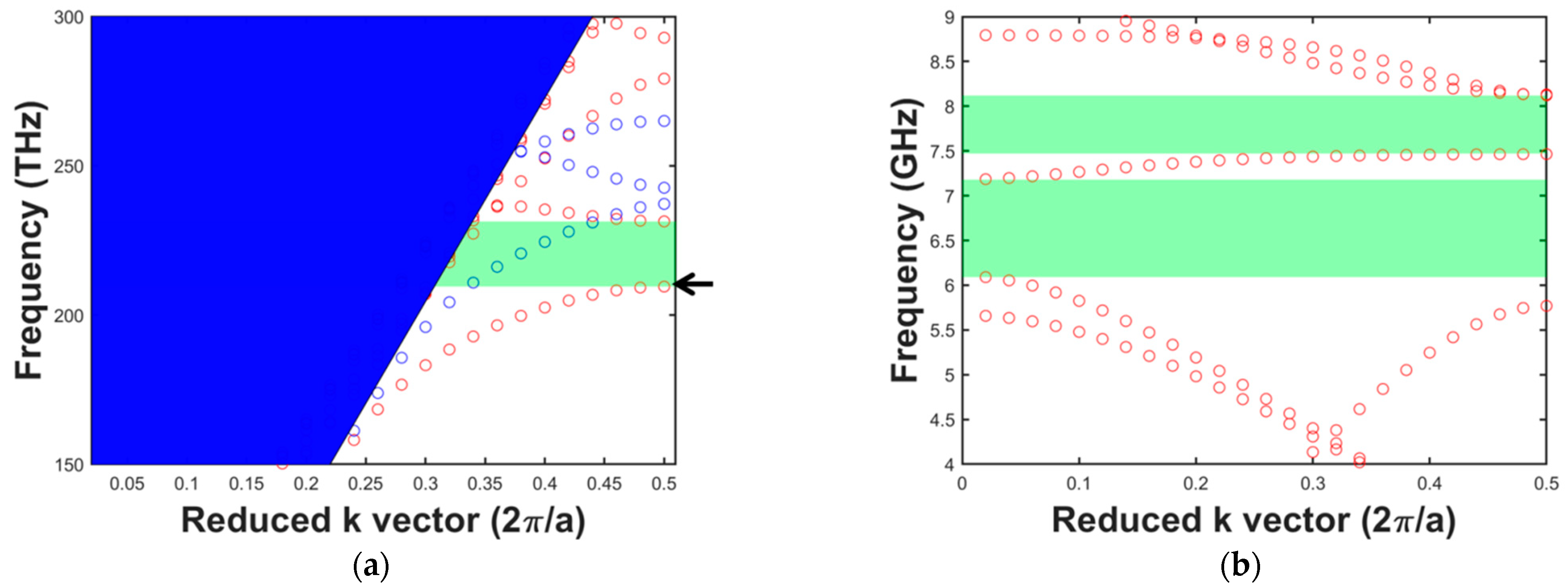
3.1. Band Structures of Photonic Crystal and Phononic Crystal

We first calculated the forbidden band gaps of PxCs. In Figure 2a,b, the PtC and PnC band structures are displayed. The horizontal axes of the band structure diagrams represent the reduced k-vector with the unit 2π/a. The reduced k-vector is defined by the k-vector normalized by the first reciprocal lattice vector lying along the direction of the wave vector. In our case, the wave vector at the Brillouin zone boundary is k = π/a. The vertical axes of the aforementioned diagrams denote the eigenfrequency. The blue region in Figure 2a represents the light line. The modes above the light line are radiative modes rather than guided modes. The red and blue circles mark the transverse magnetic (TM) and transverse electric (TE) modes in which the electric fields are parallel and perpendicular with the x-z plane in the nanobeam, respectively. Thus, a photonic band gap of the TM modes (marked by a light green color region) begins from 209.5 THz to 231.4 THz. A photonic slow light mode is marked by the arrow near the band gap edge and the frequency is 209.5 THz, the corresponding free space wavelength is about 1431 nm. The electric field in x component (Ex) of the slow light mode is shown in the inset of Figure 2a. It can be noticed that the electric field is mainly concentrated in the center of the fishbone and less in the wings. It implies that this slow light mode can exist stably in structures with different wing lengths. In Figure 2b, the PnC band gaps are illustrated by light green regions. The ranges of two phononic band gaps are 6.09–7.18 GHz and 7.47–8.12 GHz. With the existence of both the PtC band gap and PnC band gaps, we can trap not only the photonic modes but also the phononic modes into the PxC cavity simultaneously.

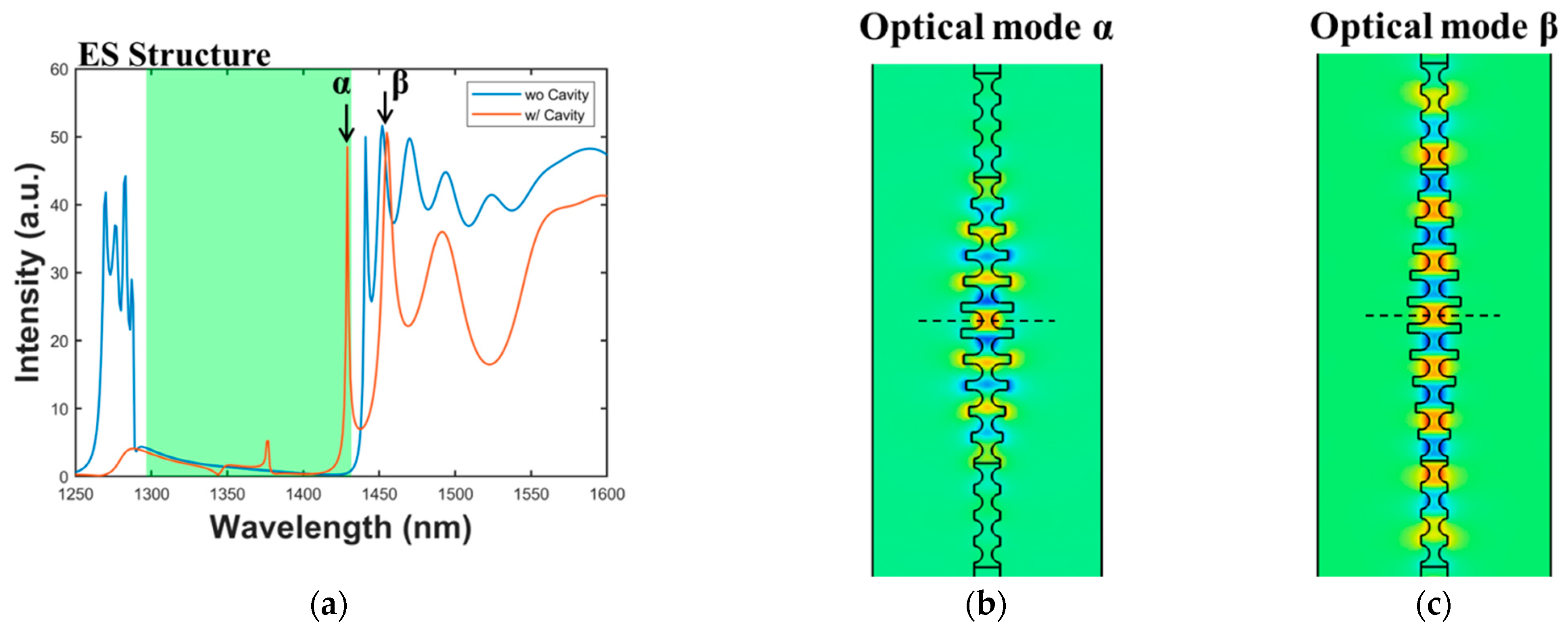
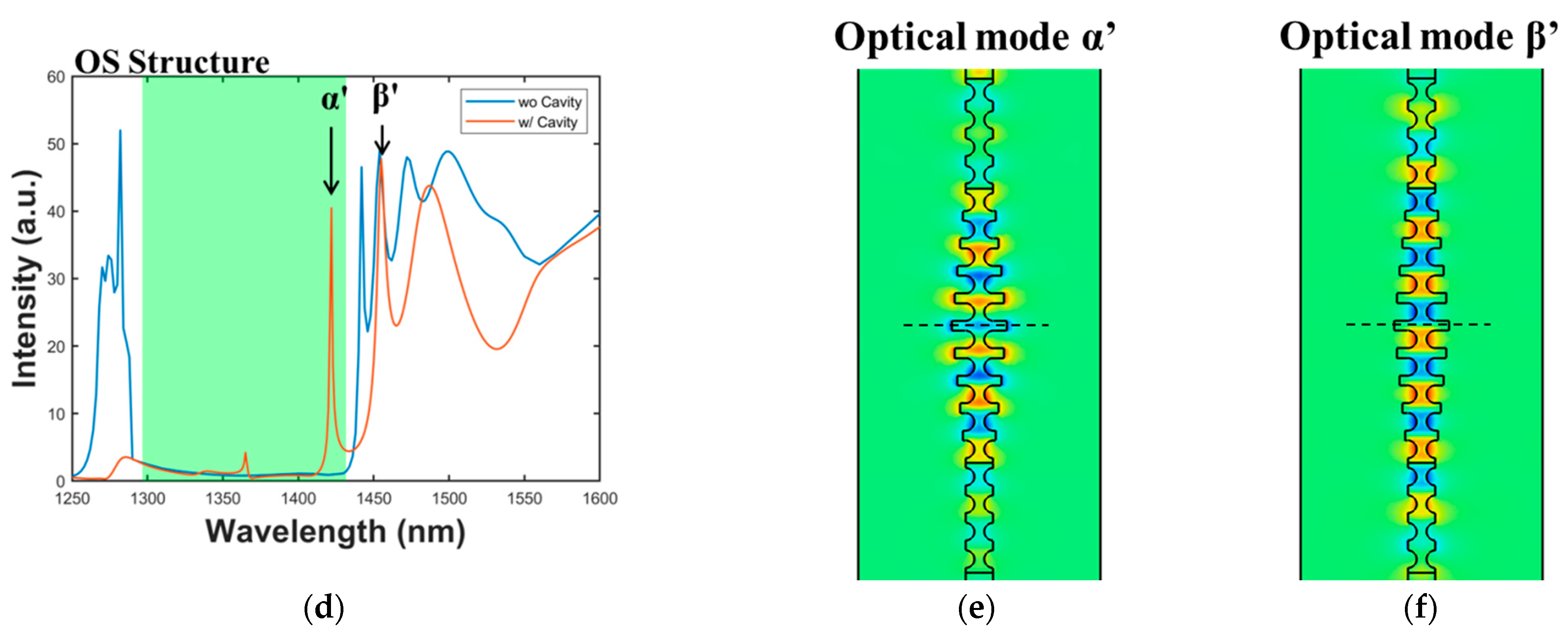
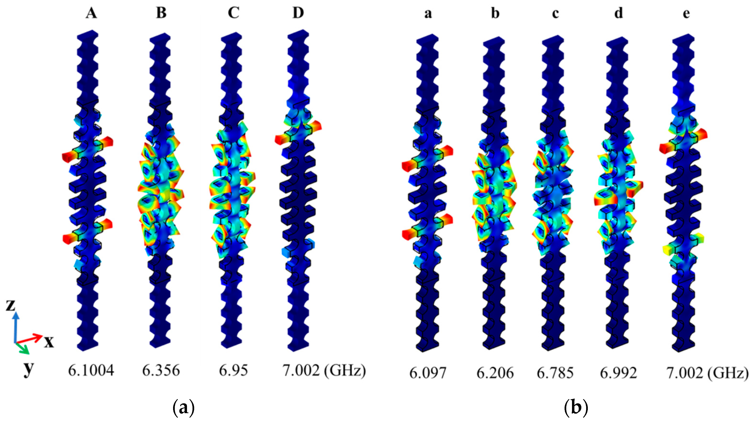
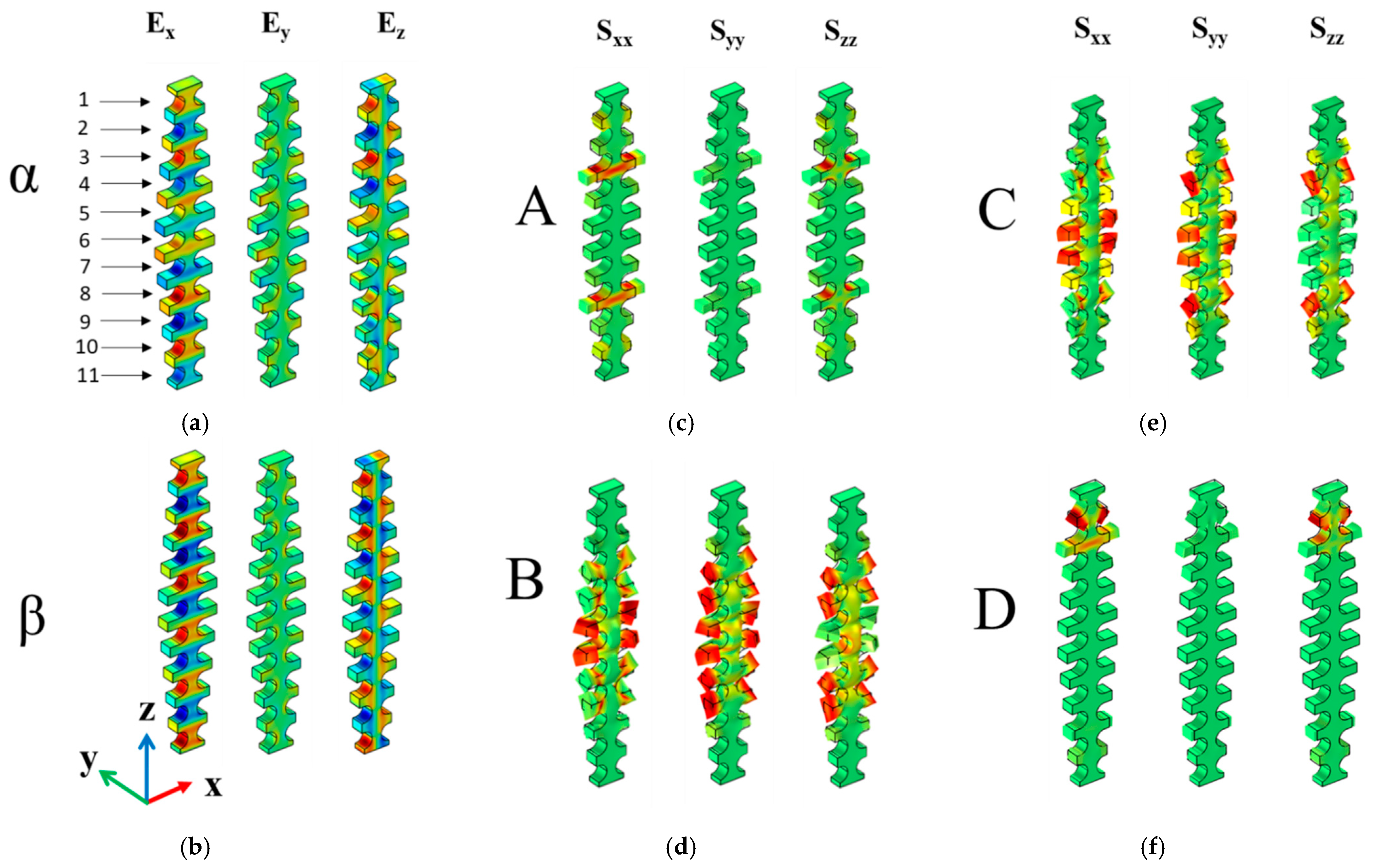
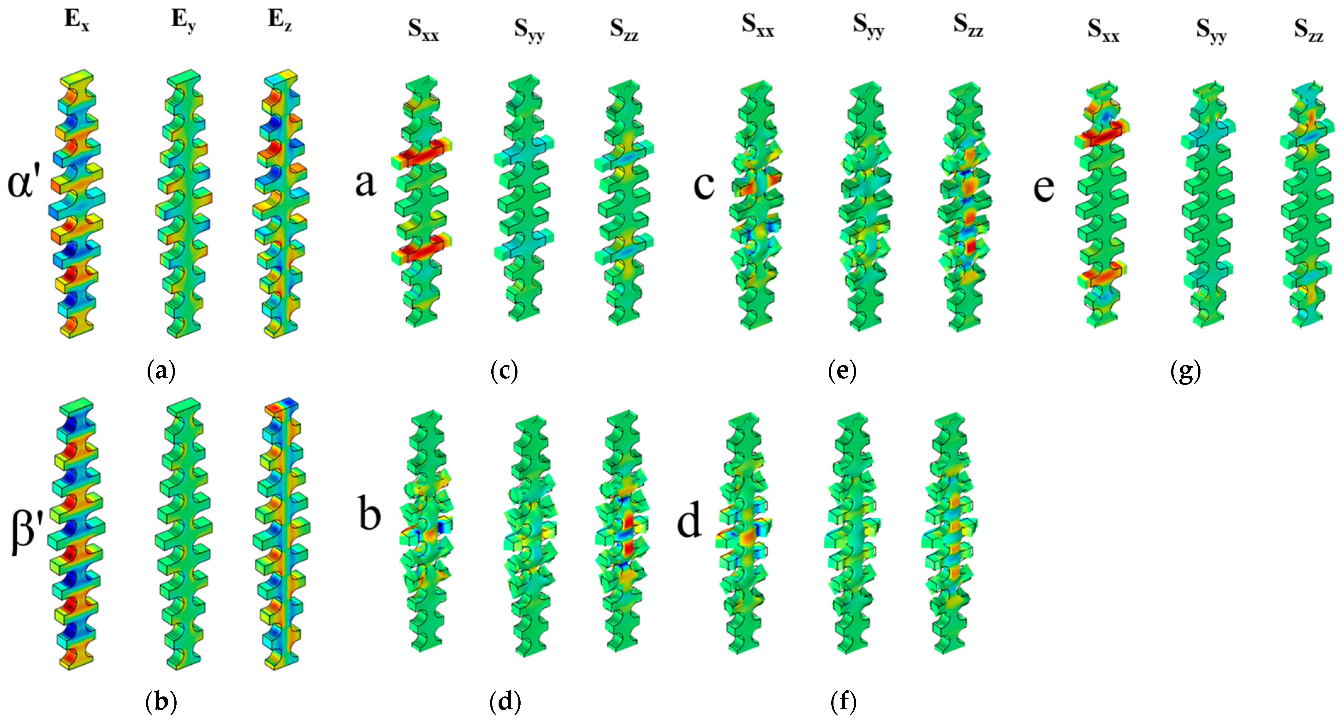
3.2. Optical and Acoustic Resonance Modes

The resonant modes of ES and OS structures can be investigated by the transmission spectra, which can be obtained by FEM frequency domain simulation. In the frequency domain simulation, the full fishbone nanobeam is placed alone in the z direction surrounded by air. A TM polarized electromagnetic wave is incident from the top of the nanobeam toward the –z direction to the bottom. Figure 3a shows the transmission spectrum of the structure in Figure 1c by the orange line. The blue line in Figure 3a is the reference transmission spectrum, which is the transmission of PtC nanobeam contents of 19 unit cells of mirror regions without any gradient varying cavity. The blue line reveals a forbidden transmission frequency band that extends from about 1300 nm to 1430 nm (light green region). The forbidden transmission frequency range agrees with the TM polarized band gap in Figure 2a. Comparing the transmission spectrum of ES structure to reference one, we can find that, in the orange line, one transmission peak (marked as α) appears inside the band gap region at wavelength 1429 nm. This is the defect mode of gradient varying cavities.
Outside the band gap region, the slow light mode that was mentioned in the band structure is marked as β. The slow light mode is observed in both orange and blue lines. The wavelength of β is 1456 nm in the orange line and 1455 nm in the blue lines. We identified the peaks β in orange and blue spectra as slow light mode because their electric field distributions are similar to the inset of Figure 2a. As mentioned before, the eigenmode of the slow light is concentrated near the center of the nanobeam, so it can be excited in both structures with and without a cavity. The wavelengths are not exactly identical with the slow light mode in the band structure, because there is a discrepancy between transmission simulation and band structure simulation. The x-component of electric fields (Ex) in the x-z plane of modes α and β are shown in Figure 3b,c. By observing the Ex distributions in Figure 3b, we can confirm that mode α is trapped by the mirror regions beside both sides of the cavity. In Figure 3c, the Ex distributes in not only within the cavity but also in the mirror regions. It shows that the mode β is a transmission mode.
On the other hand, Figure 3d illustrates the transmission spectrum of the OS structure and the reference structure, which contain 18 identical unit cells by orange line and blue line, respectively. The forbidden transmission region extends at the same frequency range shown by the blue line. From the orange line, the defect cavity mode α’ can be found at 1422 nm inside the forbidden band gap and the slow light mode β’ locates at the same wavelength at 1456 nm. The Ex fields of mode α’ and β’ in the OS structure are illustrated in Figure 3e,f. The defect cavity and slow light modes of both the ES and OS structures will be used as the optical modes in the following AO interactions for comparison.
Regarding the phononic modes, the mechanical spectra of the ES structure and OS structure within the cavity are displayed in Figure 4. Same as the simulation of PtC in Figure 3, the full fishbone nanobeam is placed alone in the z-direction. Both sides of the end of the nanobeam are fixed and mechanical force incident from additional cells outside the mirror region by a boundary load. In Figure 4a, the acoustic spectra of ES are presented by an orange line. The amplitude in the graph is the logarithmic magnitude of the average displacement field. Due to the gradient varying wing length in the cavity, some cavity modes can produce high amplitude in the spectra. Similar to the presentation in Figure 3a, the blue line represents the acoustic transmission of the reference structure, which contains 19 identical unit cells without gradient varying cavities. The acoustic transmission band gap is revealed by the light green region, which corresponds to the lower band gap region in Figure 4b. Four acoustic defect cavity modes are pointed out inside the band gap frequency range of the ES structure. These modes are located at 6.1004, 6.356, 6.95, and 7.002 GHz and are denoted as A, B, C, and D, respectively. We also performed the eigen mode simulation using the full ES structure. It confirmed that the displacement field of modes A, B, C, and D concentrate within the cavity region of the ES structure. There are several peaks other than A, B, C, and D in the orange line. However, we cannot find the corresponding eigen modes of those peaks. This implies that these peaks are not the intrinsic resonant defect cavity modes. This may result from the interference of the input end, the output end, and the interface between mirror and cavity regions.
Orange and blue lines in Figure 4b show the transmission spectra of OS structure and the reference structure, which contains only 18 unit cells without a cavity. In Figure 4b, the blue line shows that the acoustic band gap can also be observed in the range from 6.09 to 7.18 GHz. Five peaks result from acoustic defect cavity mode at 6.097, 6.206, 6.785, 6.992, and 7.002 GHz are marked by a, b, c, d, and e, respectively, in Figure 4b in the transmission band gap region. As discussed in the ES structure, these peaks can also be found in the full structure eigen modes simulation.
In order to classify the vibration behaviors of these 9 acoustic modes in Figure 4, we show the displacement fields of the eigen mode of these modes in Figure 5. Because the axis of nanobeam and wings lie on the x-z plane, we can classify these modes according to the vibration directions with respect to the x-z plane. In Figure 5a, the displacement fields of modes A, B, C, and D of the ES structure are illustrated. The modes A and D show similar deforming behaviors, and the wings are stretched and compressed only in the x-z plane along the x-direction, which is perpendicular to the axis of the nanobeam. In contrast, the deformed behaviors of mode B and C is more complicated. The wings are curved, and the ends of the wings are bent in +y and −y directions. We define the mode A and D as the in-plane shear mode, and B and C as the out-of-plane vertical modes. In Figure 5b, the deformed shape of the eigen modes a, b, c, d, and e of the OS structure are illustrated. We can classify the modes in the same manner as with Figure 5a; the modes a and e are the in-plane shear modes, and modes b, c, and d are the out-of-plane vertical modes.

3.3. AO Coupling Rate Calculations

We can now further discuss the AO coupling rate between the photonic modes and phononic modes in the aforementioned. The AO coupling rate can be described as the maximum frequency shift of a certain optical mode during the structure oscillated by a certain acoustic mode with amplitude identical to zero-point motion. The optical frequency shift results from the vibration-induced refractive index change and structure deformation. The photo-elastic (PE) effect describes the optical mode perturbed by the spatial refractive index change, which is caused by the strain field in the structure. On the other hand, the moving boundary (MB) effect describes the optical mode perturbed by the structural deformation. In our simulation, the maximum strain field is limited within 10−3 in order to ensure that each AO interaction is experimentally achievable.
The optical frequency shift caused by PE and MB effects can be calculated by Equations (1) and (2), respectively. The PE and MB effects occur simultaneously and the total optical frequency shift results from both PE and MB effects can be obtained by adding gPE and gMB (Equation (3)) [32,33,34,35].
g P E = ω 2 E | δ ε | E   E · D   d V / 2 m e f f Ω ,
g M B = ω 2   ( Q · n ^ ) ( Δ ε E 2 Δ ε 1 D 2 )   d S   E · D   d V / 2 m e f f Ω ,
g = g M B + g P E ,
where ω is the frequency of the coupling photonic mode, Q is the normalized displacement field ( m a x { | Q | = 1 }), and n ^ is the outward normal vector at the boundary. The / 2 m e f f Ω m is the zero-point motion of the PxC resonator mentioned before, where the meff is effective mass, Ω is the frequency of the phononic mode, and is the reduced Planck constant. The E & D with subscripts and , respectively represent the electric field and the electric displacement field that are parallel and perpendicular to the structure surface, and ε is the dielectric permittivity. Considering the permittivity of silicon and air, Δ ε = ε S i ε a i r and Δ ε 1 = ε S i 1 ε a i r 1 calculated the difference between the two materials. δ ε i j = ε 0 n S i 4 p i j k l S k l is the spatial permittivity distribution caused by acoustic perturbation, where nSi is the refractive index of silicon, pijkl is the photoelastic tensor, and Skl is the strain tensor [32,36]. Therefore, the photo-elastic component can be written as:
E | δ ε | E   = ε 0 n S i 4   [ 2 R e { E x * E y } p 44 S x y + 2 R e { E x * E z } p 44 S x z + 2 R e { E y * E z } p 44 S y z + | E x | 2 ( p 11 S x x + p 12 ( S y y + S z z ) ) + | E y | 2 ( p 11 S y y + p 12 ( S x x + S z z ) ) + | E z | 2 ( p 11 S z z + p 12 ( S x x + S y y ) ) ] ,
We calculated the AO coupling between each optical mode and acoustic mode of ES and OS structures in Figure 3 and Figure 4. The AO coupling rates of ES and OS structures are listed in Table 1 and Table 2, respectively. It should be noticed that the positive and negative signs of g values in Table 1 and Table 2 represent the blue and red shifting of the optical mode’s frequency. In other words, the greater the absolute value of g, gPE, and gMB, the stronger the AO interaction. The sign of the g value indicates the direction of the optical frequency shift. In Table 1, in the column of optical mode α, the AO coupling rates (g values) of acoustic in-plane shear modes (A and D) are stronger than acoustic out-of-plane vertical modes (B and C). The contribution of PE effects of acoustic modes A and D is significantly stronger than acoustic modes B and C. Meanwhile, the difference in contributions of MB effects between the in-plane modes (A and D) and the out-of-plane modes (B and C) are not obvious. We can conclude that the strong AO coupling rates of acoustic in-plane modes result from the PE effect. For the column of optical mode β in Table 1, the g values of in-plane are also greater than that of out-of-plane modes. The major contributions of AO interactions between in-plane modes and optical mode β result from the PE effect as well.

3.4. AO Coupling Rate Discussions

In order to further discuss Table 1, we show the x, y, and z components of electric fields of optical modes α and β in Figure 6a,b, respectively. We also show the normal strain fields (Sxx, Syy, and Szz) of acoustic modes A, B, C, and D in Figure 6c–f, respectively. The terms of shear strain fields in Equation (4) are one order smaller than that of normal strain fields in our simulation, so we do not show the shear strain fields here. First, we discuss the reason that the gPE values of the in-plane mode are stronger than the gPE of the out-plane mode. The p 11 in Equation (4) is one order larger than p 12 , so the PE effects are dominated by the volume integration of the products of | E i | and S i i ,   where   i = x ,   y ,   z . In other words, a strong PE effect requires a larger overlap between the | E i | fields and the S i i fields. In Figure 6a,b, the major components of the electric fields of optical modes α and β are E x and E z . The fields of E x and E z concentrate in the center of the nanobeam for both optical modes α and β. The E x fields of both optical modes are symmetric with respect to the center y-z cross-section of the nanobeam, so the field distribution in the center of the nanobeam is significant. Meanwhile, the E z fields of both optical modes are anti-symmetric with respect to the center y-z cross-section of nanobeam, so the intensities of E z fields in the center of nanobeam are very weak.
In terms of normal strain fields of acoustic mode A, Figure 6c shows that the Sxx is distributed majorly in the wings between the 3rd and 4th unit cells and between the 8th and 9th unit cells. The Szz distributes at the side walls of wings between 3rd and 4th unit cells, and the side walls of wigs between 8th and 9th unit cells. The fields of Ex of mode α and Sxx of mode A overlap between 3rd and 4th unit cells and between 8th and 9th unit cells as well as the fields of Ez and Szz. It implies that the PE effects of AO interaction between mode A and mode α are significant. By comparing Figure 6a with Figure 6f, not only the Ex and Sxx fields but also the Ez and Szz fields overlap at the 2nd unit cell. It can be concluded that the PE effect of AO interaction between mode β and mode D is also strong. On the other hand, the normal strain fields of out-of-plane modes B and C distribute majorly at the end of each wing, However, the electric fields of modes α and β are distributed mostly in the center of the nanobeam. The electric fields do not overlap the strain for out-of-plane acoustic mode and both optical modes, so the PE effects of AO interaction are weak.
Secondly, we discuss the reason that the PE effect is stronger than the MB effect in the AO interaction between acoustic in-plane modes and both optical modes α and β. According to Equation (2), the numerator is a surface integration. The first term ( Q · n ^ ) within the integration is the displacement vector’s component, which is normal for the surface. The second term is associated with electric fields. Although the second term is not intuitive, we can still conclude that the strong MB effect needs a larger displacement component, which is normal for the surface of the structure; in addition, the displacement field should overlap with the electric field. In Figure 5a, mode A, the ( Q · n ^ ) are strong at the ends of the wings between the 3rd and 4th unit cells and the ends of the wings between the 8th and 9th unit cells. However, the electric fields of both optical modes α and β concentrate at the center of the nanobeam rather than the ends of the wings, so the MB effect of AO interaction between mode A and both optical modes is not strong. A similar explanation can be applied to mode D and both optical modes.
For the acoustic out-of-plane modes B and C in Figure 5a, the ( Q · n ^ ) are large at the surfaces with normal vectors parallel to y-direction, especially at the end of wings. However, the electric fields of both optical mode α and β concentrate at the center, especially at the side wall of the semi-air cylinder. This implies that the MB effects of AO interactions are not significant.
Finally, the optical mode α is defect cavity mode and optical mode β is a slow light mode. However, the strengths of the AO interaction of these two modes do not exhibit obvious differences. This is because their electric field distributions are very similar to each other.
For OS structure, the x, y, and z components of electric fields of optical modes α’ and β’ are shown in Figure 7a,b, respectively. The normal strain fields of acoustic modes a, b, c, d, and e are shown in Figure 7c–e, respectively. The electric field distributions of Figure 7a,b are very similar to Figure 6a,b. Meanwhile, the normal strain field of Figure 7c,g is also similar to Figure 6c,e. Therefore, the strong PE effects in AO interactions between acoustic in-plane modes and both optical modes α’ and β’ can be understood in the same manner that has been discussed in the ES structure. The MB effects are weaker than the PE effects in the AO interaction between acoustic in-plane modes, and both optical modes α’ and β’ can also be explained in a similar manner to the ES structure.
In terms of AO interaction between acoustic out-of-plane modes and both optical modes, the displacement fields of acoustic modes b, c, and d concentrate at the end of wings. However, the electric fields of optical mode α’ and β’ are concentrated near the center of the nanobeam. Therefore, the MB effects of AO interaction are not significant. On the other hand, the normal strain fields of out-of-plane modes b, c, and d of OS structure are not similar to modes B and C of ES structure. The dominated normal strain fields of modes b, c, and d are Sxx and Szz. The fields of Sxx distribute at some wings and center regions of nanobeam. The fields of Szz distribute majorly at the center of the nanobeam. The Sxx and Szz overlap the x and z components of electric fields in Figure 7a,b. However, some portions of Sxx and Szz fields are positive (red in colormap) and the others are negative (blue in colormap). The positive and negative normal strains lead to a positive and negative optical frequency shift in the PE effect, so the total contributions of the PE effect on the AO interaction are neutralized. Thus, the AO coupling between acoustic out-of-plane modes and both optical modes is not strong.

4. Conclusions

We have designed an AO coupling structure with a gradient varying wing length cavity in a fishbone nanobeam. According to the symmetry type in the cavities, the fishbone nanobeams are separated into even-symmetry and odd-symmetry with a different number of periods inside the cavities. We displayed both the photonic band gap and phononic band gaps and found several modes to introduce the AO interactions. The AO interaction rates g = gPE + gMB have been discussed by two photonic modes, the defect cavity mode, which is located inside the PtC band gap and slow light mode, which is outside the band gap, coupled with four defect phononic modes for the ES structure and five defect modes for the OS structure
Our results showed that the AO coupling rates are strongly dependent on the overlap between acoustic fields and optical fields. The acoustic in-plane modes exhibited the best AO coupling rates when they interacted with both defect cavity and slow light modes. The acoustic in-plane modes are formed by stretching certain wings of a fishbone nanobeam. The stretching leads to in-phase normal strain fields in structures, which enhances the PE effects. The AO coupling rate based on stretched acoustic modes can be further improved by adjusting the geometrics of cavities for seeking acoustic modes with more stretched wings. This may increase the variety of optomechanical applications.

Author Contributions

Conceptualization, F.-L.H. and C.-C.C.; Data curation, W.-S.C. and Y.-P.T.; Formal analysis, F.-L.H. and Y.-P.T.; Funding acquisition, F.-L.H. and B.-S.L.; Investigation, W.-S.C. and C.-T.C.; Methodology, F.-L.H. and Y.-P.T.; Project administration, F.-L.H. and B.-S.L.; Resources, C.-C.C.; Software, W.-S.C. and C.-C.C.; Supervision, F.-L.H. and B.-S.L.; Validation, W.-S.C., Y.-P.T. and C.-C.C.; Visualization, C.-T.C.; Writing–original draft, W.-S.C. and Y.-P.T.; Writing–review & editing, F.-L.H., B.-S.L. and C.-T.C. All authors have read and agreed to the published version of the manuscript.

Funding

This research received no external funding.

Institutional Review Board Statement

Not applicable.

Informed Consent Statement

Not applicable.

Data Availability Statement

Not applicable.

Conflicts of Interest

The authors declare that they have no known competing financial interests or personal relationships that could have appeared to influence the work reported in this paper.

References

  1. O’Brien, J.L.; Furusawa, A.; Vučković, J. Photonic quantum technologies. Nat. Photonics 2009, 3, 687–695. [Google Scholar] [CrossRef] [Green Version]
  2. Zhang, W.; Cheng, K.; Wu, C.; Wang, Y.; Li, H.; Zhang, X. Implementing Quantum Search Algorithm with Metamaterials. Adv. Mater. 2018, 30, 1703986. [Google Scholar] [CrossRef] [PubMed] [Green Version]
  3. Rakhmanov, A.L.; Zagoskin, A.M.; Savel’ev, S.; Nori, F. Quantum metamaterials: Electromagnetic waves in a Josephson qubit line. Phys. Rev. B 2008, 77, 144507. [Google Scholar] [CrossRef] [Green Version]
  4. Stav, T.; Faerman, A.; Maguid, E.; Oren, D.; Kleiner, V.; Hasman, E.; Segev, M. Quantum entanglement of the spin and orbital angular momentum of photons using metamaterials. Science 2018, 361, 1101–1104. [Google Scholar] [CrossRef]
  5. Jin, Y.; Fernez, N.; Pennec, Y.; Bonello, B.; Moiseyenko, R.P.; Hémon, S.; Pan, Y.; Djafari-Rouhani, B. Tunable waveguide and cavity in a phononic crystal plate by controlling whispering-gallery modes in hollow pillars. Phys. Rev. B 2016, 93, 054109. [Google Scholar] [CrossRef] [Green Version]
  6. Mohammadi, S.; Eftekhar, A.A.; Hunt, W.D.; Adibi, A. High-Q micromechanical resonators in a two-dimensional phononic crystal slab. Appl. Phys. Lett. 2009, 94, 051906. [Google Scholar] [CrossRef]
  7. Notomi, M.; Tanabe, T.; Shinya, A.; Kuramochi, E.; Taniyama, H.; Mitsugi, S.; Morita, M. Nonlinear and adiabatic control of high-Q photonic crystal nanocavities. Opt. Express 2007, 15, 17458–17481. [Google Scholar] [CrossRef]
  8. Quan, Q.; Loncar, M. Deterministic design of wavelength scale, ultra-high Q photonic crystal nanobeam cavities. Opt. Express 2011, 19, 18529–18542. [Google Scholar] [CrossRef] [Green Version]
  9. Tomljenovic-Hanic, S.; Steel, M.J.; Sterke, C.M.d.; Moss, D.J. High-Q cavities in photosensitive photonic crystals. Opt. Letters 2007, 32, 542–544. [Google Scholar] [CrossRef]
  10. Eichenfield, M.; Chan, J.; Camacho, R.M.; Vahala, K.J.; Painter, O. Optomechanical crystals. Nature 2009, 462, 78–82. [Google Scholar] [CrossRef]
  11. Aboutalebi, S.Z.; Bahrami, A. Design of phoxonic filter using locally-resonant cavities. Phys. Scr. 2021, 96, 075704. [Google Scholar] [CrossRef]
  12. Amoudache, S.; Pennec, Y.; Djafari Rouhani, B.; Khater, A.; Lucklum, R.; Tigrine, R. Simultaneous sensing of light and sound velocities of fluids in a two-dimensional phoXonic crystal with defects. J. Appl. Phys. 2014, 115, 134503. [Google Scholar] [CrossRef]
  13. Jin, J.; Wang, X.; Zhan, L.; Hu, H. Strong quadratic acousto-optic coupling in 1D multilayer phoxonic crystal cavity. Nanotechnol. Rev. 2021, 10, 443–452. [Google Scholar] [CrossRef]
  14. Laude, V.; Beugnot, J.-C.; Benchabane, S.; Pennec, Y.; Djafari-Rouhani, B.; Papanikolaou, N.; Escalante, J.M.; Martinez, A. Simultaneous guidance of slow photons and slow acoustic phonons in silicon phoxonic crystal slabs. Opt. Express 2011, 19, 9690–9698. [Google Scholar] [CrossRef] [Green Version]
  15. Laude, V.; Beugnot, J.-C.; Benchabane, S.; Pennec, Y.; Djafari-Rouhani, B.; Papanikolaou, N.; Martinez, A. Design of waveguides in silicon phoxonic crystal slabs. In Proceedings of the 2010 IEEE International Ultrasonics Symposium, San Diego, CA, USA, 11–14 October 2010; pp. 527–530. [Google Scholar]
  16. Lin, T.-R.; Lin, C.-H.; Hsu, J.-C. Enhanced acousto-optic interaction in two-dimensional phoxonic crystals with a line defect. J. Appl. Phys. 2013, 113, 053508. [Google Scholar] [CrossRef]
  17. Ma, T.-X.; Wang, Y.-S.; Zhang, C. Photonic and phononic surface and edge modes in three-dimensional phoxonic crystals. Phys. Rev. B 2018, 97, 134302. [Google Scholar] [CrossRef]
  18. Ma, X.; Xiang, H.; Yang, X.; Xiang, J. Dual band gaps optimization for a two-dimensional phoxonic crystal. Phys. Lett. A 2021, 391, 127137. [Google Scholar] [CrossRef]
  19. Xia, B.; Fan, H.; Liu, T. Topologically protected edge states of phoxonic crystals. Int. J. Mech. Sci. 2019, 155, 197–205. [Google Scholar] [CrossRef]
  20. Zhang, R.; Sun, J. Design of Silicon Phoxonic Crystal Waveguides for Slow Light Enhanced Forward Stimulated Brillouin Scattering. J. Lightwave Technol. 2017, 35, 2917–2925. [Google Scholar] [CrossRef]
  21. Chiu, C.C.; Chen, W.M.; Sung, K.W.; Hsiao, F.L. High-efficiency acousto-optic coupling in phoxonic resonator based on silicon fishbone nanobeam cavity. Opt. Express 2017, 25, 6076–6091. [Google Scholar] [CrossRef]
  22. Hsiao, F.-L.; Hsieh, C.-Y.; Hsieh, H.-Y.; Chiu, C.-C. High-efficiency acousto-optical interaction in phoxonic nanobeam waveguide. Appl. Phys. Lett. 2012, 100, 171103. [Google Scholar] [CrossRef]
  23. Lei, L.; Yu, T.; Liu, W.; Wang, T.; Liao, Q. Dirac cones with zero refractive indices in phoxonic crystals. Opt. Express 2022, 30, 308–317. [Google Scholar] [CrossRef] [PubMed]
  24. Lucklum, R.; Zubtsov, M.; Oseev, A. Phoxonic crystals--a new platform for chemical and biochemical sensors. Anal. Bioanal. Chem. 2013, 405, 6497–6509. [Google Scholar] [CrossRef] [PubMed]
  25. Rolland, Q.; Oudich, M.; El-Jallal, S.; Dupont, S.; Pennec, Y.; Gazalet, J.; Kastelik, J.C.; Lévêque, G.; Djafari-Rouhani, B. Acousto-optic couplings in two-dimensional phoxonic crystal cavities. Appl. Phys. Lett. 2012, 101, 061109. [Google Scholar] [CrossRef]
  26. Shaban, S.M.; Mehaney, A.; Aly, A.H. Determination of 1-propanol, ethanol, and methanol concentrations in water based on a one-dimensional phoxonic crystal sensor. Appl. Opt. 2020, 59, 3878–3885. [Google Scholar] [CrossRef] [PubMed]
  27. Andrews, R.W.; Peterson, R.W.; Purdy, T.P.; Cicak, K.; Simmonds, R.W.; Regal, C.A.; Lehnert, K.W. Bidirectional and efficient conversion between microwave and optical light. Nat. Phys. 2014, 10, 321–326. [Google Scholar] [CrossRef] [Green Version]
  28. Stannigel, K.; Rabl, P.; Sørensen, A.S.; Zoller, P.; Lukin, M.D. Optomechanical Transducers for Long-Distance Quantum Communication. Phys. Rev. Lett. 2010, 105, 220501. [Google Scholar] [CrossRef] [Green Version]
  29. Chung, C.-J.; Xu, X.; Wang, G.; Pan, Z.; Chen, R.T. On-chip optical true time delay lines featuring one-dimensional fishbone photonic crystal waveguide. Appl. Phys. Lett. 2018, 112, 071104. [Google Scholar] [CrossRef]
  30. Yan, H.; Xu, X.; Chung, C.J.; Subbaraman, H.; Pan, Z.; Chakravarty, S.; Chen, R.T. One-dimensional photonic crystal slot waveguide for silicon-organic hybrid electro-optic modulators. Opt. Lett. 2016, 41, 5466–5469. [Google Scholar] [CrossRef]
  31. Hsu, F.-C.; Lee, C.-I.; Hsu, J.-C.; Huang, T.-C.; Wang, C.-H.; Chang, P. Acoustic band gaps in phononic crystal strip waveguides. Appl. Phys. Lett. 2010, 96, 051902. [Google Scholar] [CrossRef]
  32. El-Jallal, S.; Oudich, M.; Pennec, Y.; Djafari-Rouhani, B.; Laude, V.; Beugnot, J.-C.; Martínez, A.; Escalante, J.M.; Makhoute, A. Analysis of optomechanical coupling in two-dimensional square lattice phoxonic crystal slab cavities. Phys. Rev. B 2013, 88, 205410. [Google Scholar] [CrossRef]
  33. El-Jallal, S.; Oudich, M.; Pennec, Y.; Djafari-Rouhani, B.; Makhoute, A.; Rolland, Q.; Dupont, S.; Gazalet, J. Optomechanical interactions in two-dimensional Si and GaAs phoXonic cavities. J. Phys. Condens. Matter. 2014, 26, 015005. [Google Scholar] [CrossRef] [PubMed]
  34. Gomis-Bresco, J.; Navarro-Urrios, D.; Oudich, M.; El-Jallal, S.; Griol, A.; Puerto, D.; Chavez, E.; Pennec, Y.; Djafari-Rouhani, B.; Alzina, F.; et al. A one-dimensional optomechanical crystal with a complete phononic band gap. Nat. Commun. 2014, 5, 4452. [Google Scholar] [CrossRef] [PubMed]
  35. Oudich, M.; El-Jallal, S.; Pennec, Y.; Djafari-Rouhani, B.; Gomis-Bresco, J.; Navarro-Urrios, D.; Sotomayor Torres, C.M.; Martínez, A.; Makhoute, A. Optomechanic interaction in a corrugated phoxonic nanobeam cavity. Phys. Rev. B 2014, 89, 245122. [Google Scholar] [CrossRef] [Green Version]
  36. Yariv, A.; Yeh, P. Optical Waves in Crystals; Wiley: New York, NY, USA, 1984. [Google Scholar]
Figure 1. Schematic of (a) 1D phoxonic crystal nanobeam cavity, (b) unit cell, (c) even symmetric cavity, and (d) odd symmetric cavity.
Crystals 12 00890 g001
Figure 2. Band structures of the basis unit cell in the mirror region: (a) Optical photonic band structures of the mirror. Blue dotted lines mark the transverse electric modes. (b) Phononic band structure.
Crystals 12 00890 g002
Figure 3. Simulation results for an even symmetric cavity (orange) and a reference with no defective region (blue): (a) optical transmission spectra, and the X-direction component of a normalized electric field of (b) cavity resonance mode α and (c) slow light resonance mode β. Simulation results for the odd symmetric cavity (orange) and a reference with no defective region (blue): (d) optical transmission spectra, and the X-direction component of a normalized electric field of (e) cavity resonance mode α’ and (f) slow light resonance mode β’.
Crystals 12 00890 g003aCrystals 12 00890 g003b
Figure 4. Acoustic transmission spectra (orange) and a reference with no defective region (blue) for (a) even symmetric cavity with 4 resonance modes marked by A, B, C, and D, and (b) odd symmetric cavity with 5 resonance mode marked by a, b, c, d, and e.
Crystals 12 00890 g004
Figure 5. Displacement fields of acoustic resonance modes for (a) even symmetric cavity with 4 resonance modes: A, B, C, and D, and (b) odd symmetric cavity with 5 resonance modes: a, b, c, d, and e.
Crystals 12 00890 g005
Figure 6. Distributions for the ES structures: Electric fields in x, y, z components of (a) the defect mode α and (b) slow light mode β, and the strain fields of (c) acoustic resonance mode A, (d) B, (e) C, and (f) D. The index of unit cells is marked by 1–11 in (a).
Crystals 12 00890 g006
Figure 7. Distributions for the OS structures: Electric fields in x, y, z components of (a) the defect mode α and (b) slow light mode β, and the strain fields of (c) acoustic resonance mode a, (d) b, (e) c, (f) d, and (g) e.
Crystals 12 00890 g007
Table 1. Total AO coupling rates (in MHz) between optical resonance mode and acoustic resonance modes in even symmetric cavity when both PE and MB effects are considered.
Acoustic
Modes
Optics Modes
αβ
AgPE−1.4923−1.1245
gMB−0.15400.2934
g−1.6463−0.8311
BgPE−0.0104−0.0018
gMB−0.2095−0.0914
g−0.2199−0.0932
CgPE−0.2274−0.184
gMB−0.1409−0.030
g−0.3683−0.214
DgPE0.98480.7641
gMB0.05010.1958
g1.03490.9599
Table 2. Total AO coupling rates (in MHz) between optical resonance mode and acoustic resonance modes in the odd symmetric cavity when both PE and MB effects are considered.
Acoustic
Modes
Optics Modes
α’β’
agPE1.77911.234
gMB0.1429−0.297
g1.9220.937
bgPE0.0040−0.0017
gMB−0.2259−0.0603
g−0.2219−0.0620
cgPE−0.0172−0.0746
gMB−0.2569−0.0222
g−0.2741−0.0968
dgPE−0.2694−0.1995
gMB−0.1954−0.0868
g−0.4648−0.2863
egPE1.53391.1256
gMB0.11350.2892
g1.64741.4148
Publisher’s Note: MDPI stays neutral with regard to jurisdictional claims in published maps and institutional affiliations.

