
Perovskite Photo-Sensors with Solution-Processed TiO2 under Low Temperature Process and Ultra-Thin Polyethylenimine Ethoxylated as Electron Injection Layer

Abstract
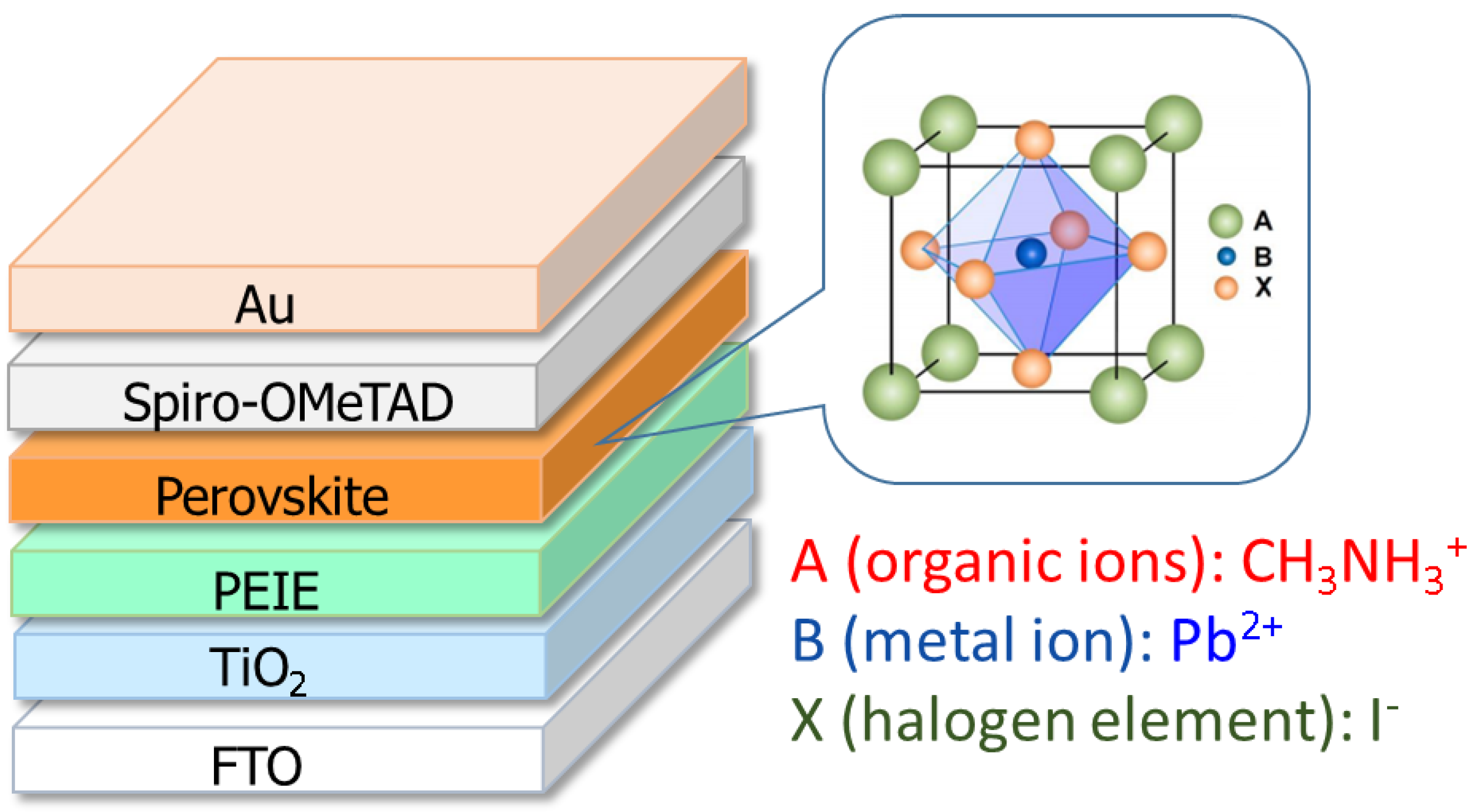
:1. Introduction
2. Experimental Section
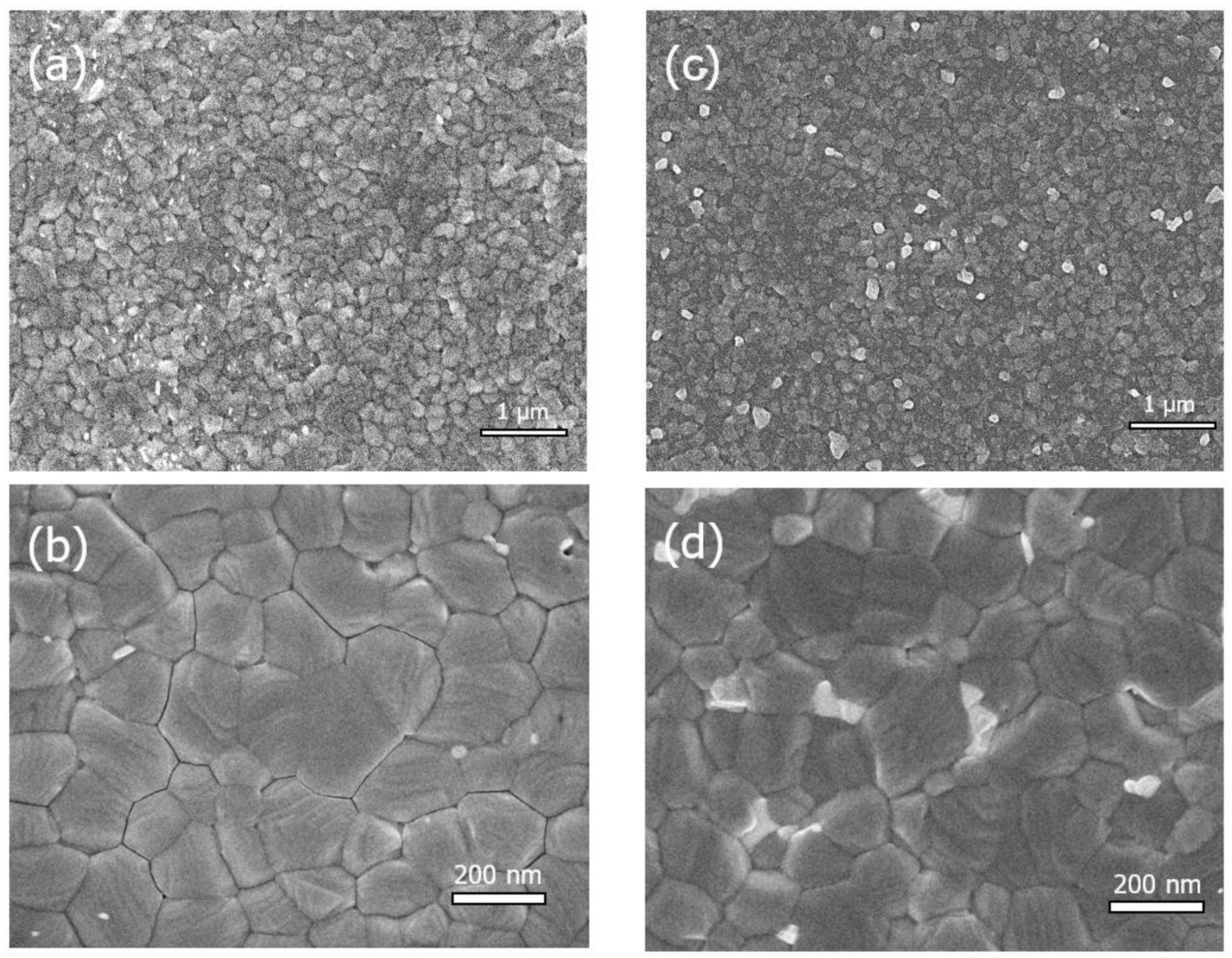
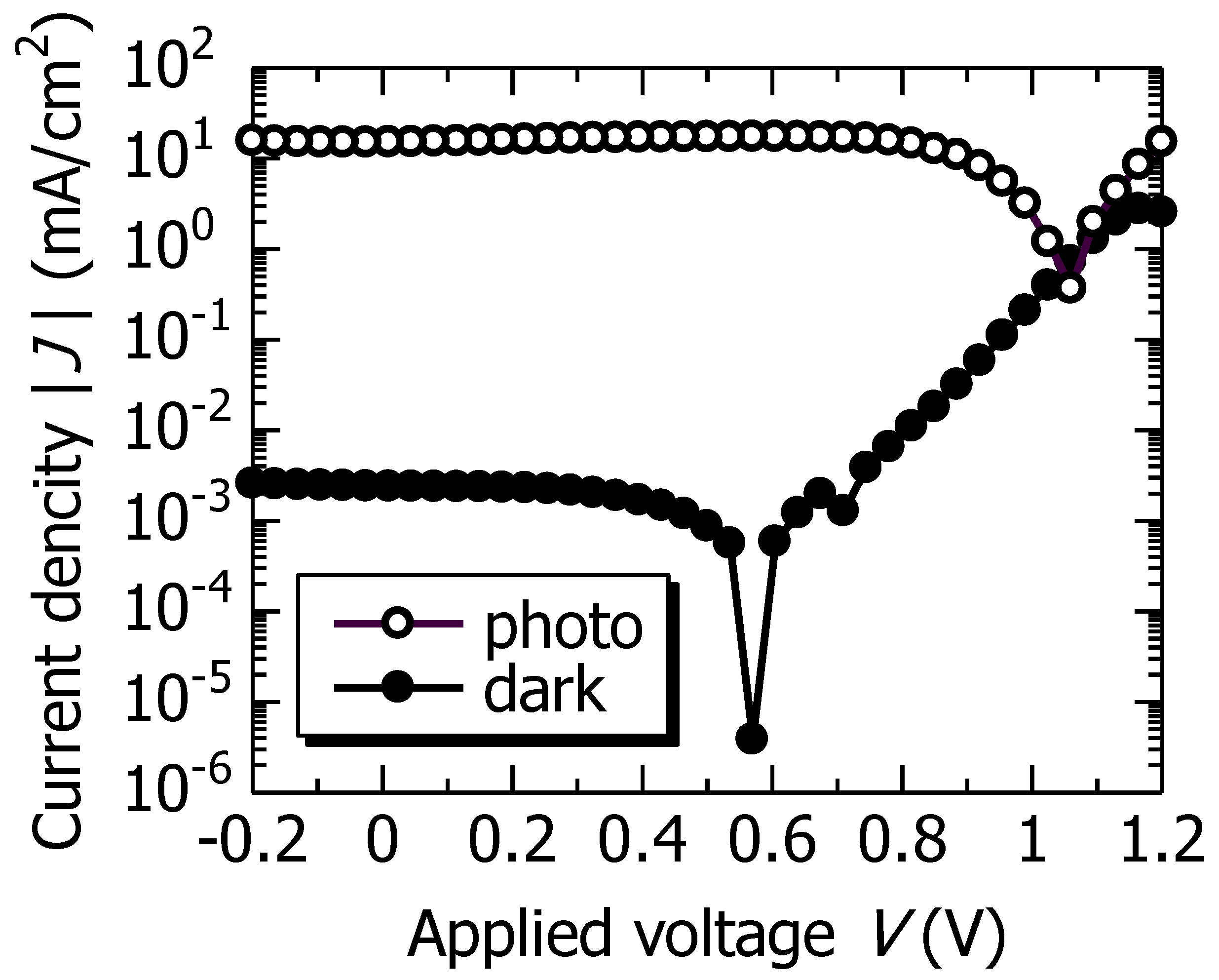
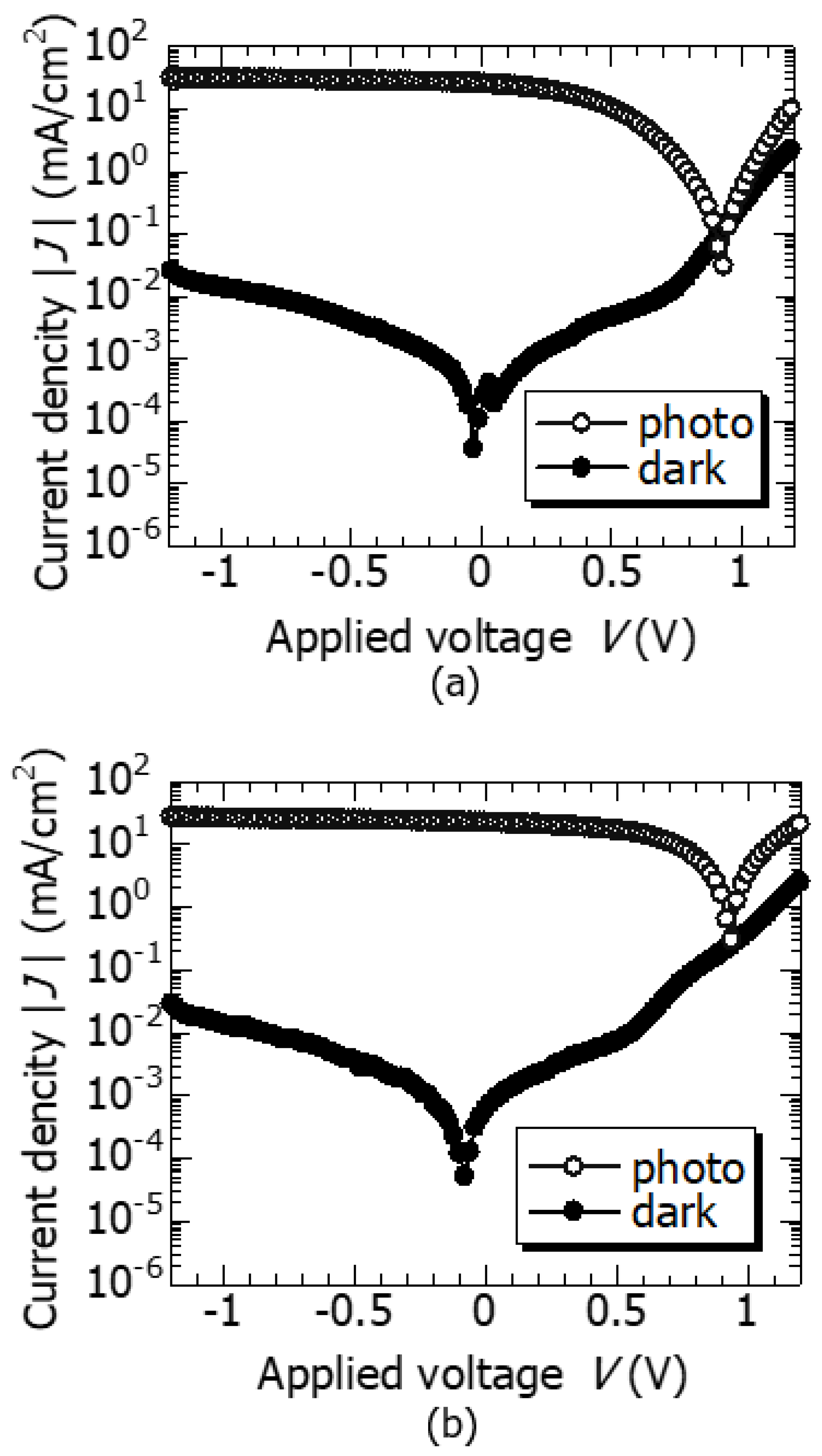
3. Results and Discussions
4. Conclusions
Author Contributions
Funding
Data Availability Statement
Acknowledgments
Conflicts of Interest
References
- Tang, C.W.; VanSlyke, S.A. Organic electroluminescent diodes. Appl. Phys. Lett. 1987, 51, 913. [Google Scholar] [CrossRef]
- Adachi, C.; Baldo, M.A.; Thompson, M.E.; Forrest, S.R. Nearly 100% internal phosphorescence efficiency in an organic light-emitting device. Appl. Phys. Lett. 2001, 90, 5048. [Google Scholar]
- Endo, A.; Ogasawara, M.; Takahashi, A.; Yokoyama, D.; Kato, Y.; Adachi, C. Thermally Activated Delayed Fluorescence from Sn4+–Porphyrin Complexes and Their Application to Organic Light Emitting Diodes—A Novel Mechanism for Electroluminescence. Adv. Mater. 2009, 21, 4802. [Google Scholar] [CrossRef] [PubMed]
- Kudo, K.; Yamashina, M.; Morizumi, T. Field Effect Measurement of Organic Dye Films. Jpn. J. Appl. Phys. 1984, 23, 130. [Google Scholar] [CrossRef]
- Tsumura, A.; Koezuka, H.; Ando, T. Macromolecular electronic device: Field-effect transistor with a polythiophene thin film. Appl. Phys. Lett. 1986, 49, 1210. [Google Scholar] [CrossRef]
- Lin, Y.-Y.; Gundlach, D.I.; Nelson, S.F.; Jackson, T.N. Pentacene-based organic thin-film transistors. IEEE Trans. Electron Devices 1997, 44, 1325. [Google Scholar] [CrossRef]
- Hyodo, T.; Morita, F.; Naka, S.; Okada, H.; Onnagawa, H. Self-Aligned Organic Field-Effect Transistors Using Back-Surface Exposure Method. Jpn. J. Appl. Phys. 2004, 43, 2323. [Google Scholar] [CrossRef]
- Katsuhara, M.; Yagi, I.; Yumoto, A.; Noda, M.; Hirai, N.; Yasuda, R.; Moriwaki, T.; Ushikura, S.; Imaoka, A.; Urabe, T.; et al. A flexible OLED display with an OTFT backplane made by scalable manufacturing process. SID 2010, 18, 399. [Google Scholar] [CrossRef]
- Yu, G.; Wang, J.; McElvain, J.; Heeger, A.J. Large-Area, Full-Color Image Sensors Made with Semiconducting Polymers. Adv. Mater. 1998, 10, 1431. [Google Scholar] [CrossRef]
- Ng, T.N.; Wong, W.S.; Chabinyc, M.L.; Sambandan, S.; Street, R.A. Flexible image sensor array with bulk heterojunction organic photodiode. Appl. Phys. Lett. 2008, 92, 213303. [Google Scholar] [CrossRef]
- Zukawa, T.; Naka, S.; Okada, H.; Onnagawa, H.J. Organic heterojunction phototransistor. Appl. Phys. 2002, 91, 1171. [Google Scholar] [CrossRef]
- Tang, C.W. Two-layer organic photovoltaic cell. Appl. Phys. Lett. 1986, 48, 183. [Google Scholar] [CrossRef]
- Yu, G.; Heeger, A.J. Charge separation and photovoltaic conversion in polymer composites with internal donor/acceptor heterojunctions. J. Appl. Phys. 1995, 78, 4510. [Google Scholar] [CrossRef]
- Meng, L.; Zhang, Y.; Wan, X.; Li, C.; Zhang, X.; Wang, Y.; Ke, X.; Xiao, Z.; Ding, L.; Xia, R.; et al. Organic and solution-processed tandem solar cells with 17.3% efficiency. Science 2018, 361, 1094. [Google Scholar] [CrossRef] [Green Version]
- Kojima, A.; Teshima, K.; Shirai, Y.; Miyasaka, T.J. Organometal Halide Perovskites as Visible-Light Sensitizers for Photovoltaic Cells. Am. Chem. Soc. 2009, 131, 6050. [Google Scholar] [CrossRef] [PubMed]
- NREL. Available online: https://www.nrel.gov/pv/cell-efficiency.html (accessed on 15 June 2022).
- Rojas, D.M.; Sun, H.; Iza, D.C.; Weickert, J.; Chen, L.; Wang, H.; Schmidt-Mende, L.; MacManus-Driscol, J.L. High-speed atmospheric atomic layer deposition of ultra thin amorphous TiO2 blocking layers at 100 C for inverted bulk heterojunction solar cells. Progr. Photovolt. 2013, 21, 393. [Google Scholar] [CrossRef] [Green Version]
- Weerasinghe, H.C.; Franks, G.V.; Plessis, J.D.; Simona, G.P.; Cheng, Y.-B. Anomalous rheological behavior in chemically modified TiO2 colloidal pastes prepared for flexible dye-sensitized solar cells. J. Photochem. Photobiol. A 2010, 213, 30. [Google Scholar] [CrossRef]
- Gong, J.; Liang, J.; Sumathy, K. Review on dye-sensitized solar cells (DSSCs): Fundamental concepts and novel materials. Renew. Sustain. Energy Rev. 2012, 16, 5848. [Google Scholar] [CrossRef]
- Li, D.; Dong, G.; Li, W.; Wang, L. High performance organic-inorganic perovskite-optocoupler based on low-voltage and fast response perovskite compound photodetector. Sci. Rep. 2015, 5, 7902. [Google Scholar] [CrossRef] [Green Version]
- Lin, Q.; Armin, A.; Lyons, D.M.; Burn, P.L.; Meredith, P. Low noise, IR-blind organohalide perovskite photodiodes for visible light detection and imaging. Adv. Mater. 2015, 27, 2060. [Google Scholar] [CrossRef]
- Chen, H.-W.; Sakai, N.; Sanehira, A.K.J.Y.; Ikegami, M.; Ho, K.-C.; Miyasaka, T.J. A switchable high-sensitivity photodetecting and photovoltaic device with perovskite absorber. Phys. Chem. Lett. 2015, 6, 1773. [Google Scholar] [CrossRef] [PubMed]
- Sutherland, B.R.; Johnston, A.K.; Ip, A.H.; Xu, J.; Adinolfi, V.; Kanjanaboos, P.; Sargent, E.H. Sensitive, fast, and stable perovskite photodetectors exploiting interface engineering. ACS Photonics 2015, 2, 1117. [Google Scholar] [CrossRef]
- Fang, Y.; Huang, J. Resolving Weak Light of Sub-picowatt per Square Centimeter by Hybrid Perovskite Photodetectors Enabled by Noise Reduction. Adv. Mater. 2015, 27, 2804–2810. [Google Scholar] [CrossRef] [PubMed]
- Yakunin, S.; Sytnyk, M.; Kriegner, D.; Shrestha, S.; Richter, M.; Matt, G.J.; Azimi, H.; Brabec, C.J.; Stangl, J.; Kovalenko, M.V.; et al. Detection of X-ray photons by solution-processed lead halide perovskites. Nat. Photonics 2015, 9, 444. [Google Scholar] [CrossRef] [PubMed]
- Dong, R.; Fang, Y.; Chae, J.; Dai, J.; Xiao, Z.; Dong, Q.; Yuan, Y.; Centrone, A.; Zeng, X.C.; Huang, J. High-gain and low-driving-voltage photodetectors based on organolead triiodide perovskites. Adv. Mater. 2015, 27, 1912. [Google Scholar] [CrossRef]
- Song, J.; Xu, L.; Li, J.; Xue, J.; Dong, Y.; Li, X.; Zeng, H. Monolayer and few-layer all-inorganic perovskites as a new family of two-dimensional semiconductors for printable optoelectronic devices. Adv. Mater. 2016, 28, 4861. [Google Scholar] [CrossRef]
- Wu, W.; Wang, X.; Han, X.; Yang, Z.; Gao, G.; Zhang, Y.; Hu, J.; Tan, Y.; Pan, A.; Pan, C. Flexible photodetector arrays based on patterned CH3NH3PbI3−xClx perovskite film for real-time photosensing and imaging. Adv. Mater. 2019, 31, 1805913. [Google Scholar] [CrossRef]
- Zhang, C.-C.; Yuan, S.; Lou, Y.-H.; Liu, Q.-W.; Li, M.; Okada, H.; Wang, Z.-K. Perovskite films with reduced interfacial strains via a molecular-level flexible interlayer for photovoltaic application. Adv. Mater. 2020, 2020, 2001479. [Google Scholar] [CrossRef]
- Xiong, T.; Wang, F.; Qiao, X.; Ma, D. A soluble nonionic surfactant as electron injection material for high-efficiency inverted bottom-emission organic light emitting diodes. Appl. Phys. Lett. 2008, 93, 123310. [Google Scholar] [CrossRef]
- Zhou, Y.; Fuentes-Hernandez, C.; Shim, J.; Meyer, J.; Giordano, A.J.; Li, H.; Winget, P.; Papadopoulos, T.; Cheun, H.; Kim, J.; et al. A universal method to produce low–work function electrodes for organic electronics. Science 2012, 336, 327. [Google Scholar] [CrossRef]
- Shoda, K.; Morimoto, M.; Naka, S.; Okada, H. Semitransparent Organic Solar Cells with Polyethylenimine Ethoxylated Interfacial Layer Using Lamination Process. IEICE Trans. Electron. 2019, 102, 196. [Google Scholar] [CrossRef]
- Morimoto, M.; Yoshida, T.; Naka, S.; Okada, H. Characteristics of electron injection at the oxide electrode/polyethylenimine ethoxylated/Alq3 interface. Jpn. J. Appl. Phys. 2020, 59, SDDC03. [Google Scholar] [CrossRef]
- Hirano, I.; Takano, R.; Zhang, C.; Okada, H. Study on Perovskite Photo-sensors with Solution-Processed Compact TiO2 Under Low Temperature Fabrication Process. In Proceedings of the 27th International Workshop on Active-Matrix Flatpanel Displays and Devices, Kyoto, Japan, 1–4 September 2020; p. 6. [Google Scholar] [CrossRef]
- Hossain, M.F.; Hirano, I.; Naka, S.; Okada, H. Evaluation of Perovskite Photo-sensors with Electron-beam Evaporated Titanium Dioxide Films. In Proceedings of the 26th International Workshop on Active-Matrix Flatpanel Displays and Devices, Kyoto, Japan, 2–5 July 2019; p. 19. [Google Scholar] [CrossRef]
- Hossain, M.F.; Naka, S.; Okada, H.J. Annealing effect of E-beam evaporated TiO2 films and their performance in perovskite solar cells. Photochem. Photobiol. A Chem. 2018, 360, 109. [Google Scholar] [CrossRef]
- Im, J.-H.; Kim, H.-S.; Parka, N.-G. Morphology-photovoltaic property correlation in perovskite solar cells: One-step versus two-step deposition of CH3NH3PbI3. APL Mater. 2014, 2, 081510. [Google Scholar] [CrossRef] [Green Version]
- Wang, M.; Feng, Y.; Bian, J.; Liu, H.; Shi, Y. A comparative study of one-step and two-step approaches for MAPbI3 perovskite layer and its influence on the performance of mesoscopic perovskite solar cell. Chem. Phys. Lett. 2018, 692, 44. [Google Scholar] [CrossRef]
- Ahmadian-Yazdi, M.R.; Zabihi, F.; Habibi, M.; Eslamian, M. Effects of process parameters on the characteristics of mixed-halide perovskite solar cells fabricated by one-step and two-step sequential coating. Nanoscale Res. Lett. 2016, 11, 408. [Google Scholar] [CrossRef] [Green Version]
- Zhang, C.-C.; Lou, Y.-H.; Li, M.; Okada, H.; Wang, Z.-K. Electric-field-manipulated crystal stacking for high-quality organic–inorganic halide perovskites. Appl. Phys. Express 2020, 13, 085503. [Google Scholar] [CrossRef]
- Shi, D.; Adinolfi, V.; Comin, R.; Yuan, M.; Alarousu, E.; Buin, A.; Chen, Y.; Hoogland, S.; Rothenberger, A.; Katsiev, K.; et al. Low trap-state density and long carrier diffusion in organolead trihalide perovskite single crystals. Science 2015, 347, 519–522. [Google Scholar] [CrossRef] [Green Version]
- Dongaonkar, S.; Servaites, J.D.; Ford, G.M.; Loser, S.; Moore, J.; Gelfand, R.M.; Mohseni, H.; Hillhouse, H.W.; Agrawal, R.; Ratner, M.A.; et al. Universality of non-Ohmic shunt leakage in thin-film solar cells. J. Appl. Phys. 2010, 108, 124509. [Google Scholar] [CrossRef]


Publisher’s Note: MDPI stays neutral with regard to jurisdictional claims in published maps and institutional affiliations. |
© 2022 by the authors. Licensee MDPI, Basel, Switzerland. This article is an open access article distributed under the terms and conditions of the Creative Commons Attribution (CC BY) license (https://creativecommons.org/licenses/by/4.0/).
Share and Cite
Hirano, I.; Maruyama, K.; Zhang, C.; Okada, H. Perovskite Photo-Sensors with Solution-Processed TiO2 under Low Temperature Process and Ultra-Thin Polyethylenimine Ethoxylated as Electron Injection Layer. Crystals 2022, 12, 914. https://doi.org/10.3390/cryst12070914
Hirano I, Maruyama K, Zhang C, Okada H. Perovskite Photo-Sensors with Solution-Processed TiO2 under Low Temperature Process and Ultra-Thin Polyethylenimine Ethoxylated as Electron Injection Layer. Crystals. 2022; 12(7):914. https://doi.org/10.3390/cryst12070914
Chicago/Turabian StyleHirano, Ikuma, Kazuya Maruyama, Congcong Zhang, and Hiroyuki Okada. 2022. "Perovskite Photo-Sensors with Solution-Processed TiO2 under Low Temperature Process and Ultra-Thin Polyethylenimine Ethoxylated as Electron Injection Layer" Crystals 12, no. 7: 914. https://doi.org/10.3390/cryst12070914
APA StyleHirano, I., Maruyama, K., Zhang, C., & Okada, H. (2022). Perovskite Photo-Sensors with Solution-Processed TiO2 under Low Temperature Process and Ultra-Thin Polyethylenimine Ethoxylated as Electron Injection Layer. Crystals, 12(7), 914. https://doi.org/10.3390/cryst12070914