Article

Cathodoluminescence of Ultrathin InAs Layers Embedded in GaAs Matrix

1
Department of Physics, Baoding University, Baoding 071000, China
2
Department of Science and Research, Baoding University, Baoding 071000, China
3
Hebei Key Laboratory of Optic-Electronic Information and Materials, College of Physics Science & Technology, Hebei University, Baoding 071002, China
*
Authors to whom correspondence should be addressed.
Crystals 2022, 12(9), 1225; https://doi.org/10.3390/cryst12091225
Submission received: 26 July 2022 / Revised: 15 August 2022 / Accepted: 26 August 2022 / Published: 31 August 2022
(This article belongs to the Special Issue Semiconductor Nanocrystals)

Abstract

:
Ultrathin InAs layers with different thicknesses, from 0.75 to 1.4 monolayer, are grown in the GaAs matrix by molecular beam epitaxy on GaAs (001) substrates. For sub-monolayer heterostructures, islands or segregations exist during the growth process. Taking advantage of the high spatial resolution of focused electron beams, cathodoluminescence measurements obtain a smaller excitation spot than conventional photoluminescence. Based on the change on the peak position, line width, and intensity, cathodoluminescence spectra indicate that the size, geometry, and roughness develop with the InAs content. Moreover, spatial discontinuities of ultrathin InAs layers are observed on spectrum images and transmission electron microscopy images. This research reveals the correlation between the optical and structural properties of ultrathin InAs layers.

1. Introduction

During the past few decades, ultrathin InAs quantum nanostructures, such as quantum dots and quantum wells, have attracted much interest in investigations of fundamental physics, electronic engineering, or optoelectronic devices [1,2,3]. It has been reported that sub-monolayer InAs grown on GaAs by the Stranski-Krastanov (SK) mode achieves an especially outstanding carrier confinement [4,5]. Depending on the change of energy and entropy, the transition to three-dimensional islands occurs in the SK heteroepitaxial growth [6]. Therefore, nanostructures of islands or segregations will be expected on ultrathin InAs layers [6,7]. For carriers, the lateral confinement of structural geometry plays a significant role for optical behaviors [8,9].
Conventionally, the optical emission of III-V semiconductor devices is investigated by photoluminescence (PL). For example, the excitation intensity dependence of PL reveals various carrier recombination channels for samples with different thicknesses of InAs layers [10]. However, the spot diameter of focused laser beams for PL measurements is usually in the order of micrometers, which is much larger than the size of most InAs nanostructures. Consequently, the optical information of PL must be treated as an average photonic behavior of ensemble nanostructures across a relatively wide area. For nanostructures buried beneath cap layers, the structural information is not revealed with the PL result. When increasing the Indium deposition, whether the PL behavior relates to the chemical intermixing or corresponds to the development of structural geometry is still under debate. Herein, we aim to employ cathodoluminescence (CL) to investigate the nanostructures on ultrathin InAs layers that are embedded inside the GaAs matrix [11]. Taking advantage of the excellent focusing ability of the electron beam, the incident beam size of CL is about 5–10 nm [12]. Although the electron beam expands rapidly inside the material due to the interaction between electrons and atoms, the excitation cross-section on the InAs layer is still lower than one micrometer. If an island or segregation exists on ultrathin InAs layers, the discontinuity of the CL signal could be observed. As a result, the CL investigation captures more information about the relationship between optical emission and structural fluctuation [13,14].
In this work, we present samples of ultrathin InAs nanostructures with the thickness of a monolayer (ML) or sub-monolayer. To observe the discontinuous optical property dependence on tiny structural variations, both CL spectra and spectrum images are acquired for inference. The evolutions of crystallinity and structural size are obtained by high-resolution X-ray diffraction (HRXRD) and transmission electron microscopy (TEM), respectively. Moreover, in relation to deeper ground states and larger capture cross sections [15], it has been deduced that a larger average lateral size of nanostructures in higher ML InAs samples should capture more carriers.

2. Materials and Methods

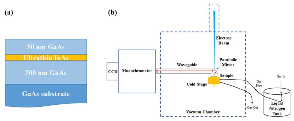
2.1. Growth of Samples

Samples with ultrathin InAs nanostructures were grown by molecular beam epitaxy (MBE) on conventional GaAs (001) substrates, as indicated in Figure 1a. The GaAs buffer layer with a 500 nm thickness was firstly grown at 580 °C after the oxide desorption process. Then, the temperature was decreased to 460 °C for the growth of InAs layers at an As4 beam equivalent pressure of 4 × 10⁻⁶ Torr. The InAs deposition rate was fixed at 0.05 ML/s for all samples. By controlling the growth time, InAs layers with different thicknesses were prepared, including 0.75 ML, 1.0 ML, 1.2 ML, and 1.4 ML. Subsequently, a 5 nm GaAs layer was grown at the same temperature after 15 s growth interruption. Finally, the growth temperature was increased back to 580 °C and another 45 nm GaAs layer was grown to complete the cap layer. All samples were named based on the calculated average InAs thickness.

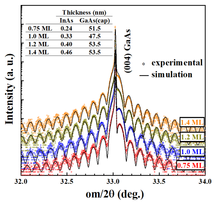
2.2. Characterization and Simulation

The CL measurement was conducted within a FEI Nova Nano SEM450 system (Hillsboro, OR, USA), as shown in Figure 1b. By selecting the scanning mode of the electron beam, high-energy electrons could excite at a point, along a line, or across an area. The emitted light would be collected by a parabolic mirror and transferred to a monochromator. After being detected by a CCD camera, either spectra or spectrum images would be provided. The sample holder, also known as a cold stage, was connected to a gas tube, which passed through an external liquid nitrogen tank. Consequently, with the flowing of nitrogen gas inside the tube, the temperature of the cold stage and samples would be brought down to 80 K. On the other hand, HRXRD patterns were obtained by a PANalytical X’Pert Pro MRD XL diffractometer (Malvern, UK) associated with a 4-bounce (220) Ge monochromator and a 3-bounce (022) Ge analyzer. M eanwhile, cross-sectional TEM images were acquired by a Cs corrected FEI Titan 80-300 equipment (Hillsboro, OG, USA) with a Schottky field emission gun operated at 300 KV. Moreover, the CASINO Monte Carlo simulation (ver 2.51, Dr. Drouin, University of Usherbrooke, CA) was applied to indicate the trajectories of electrons inside materials.

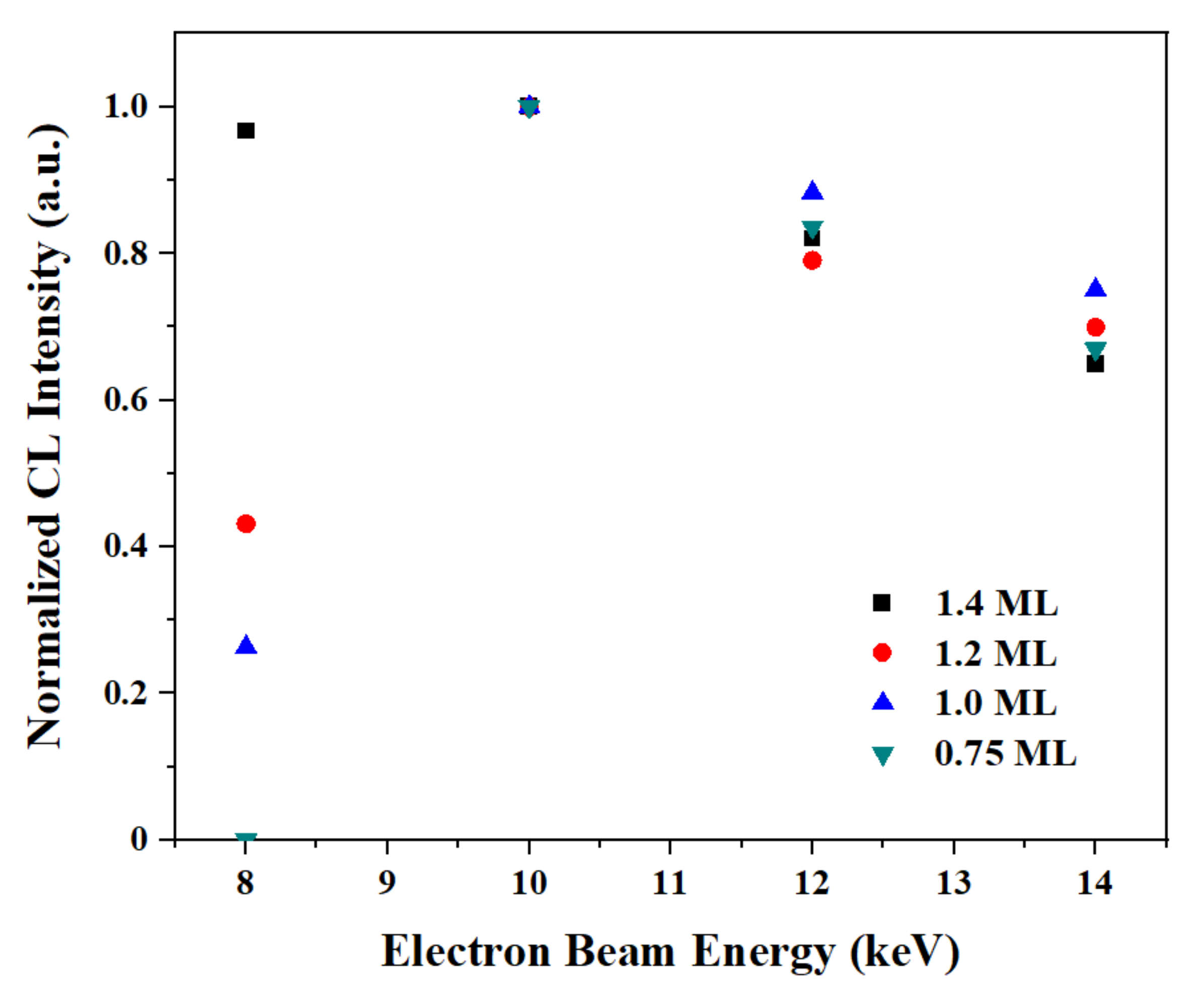
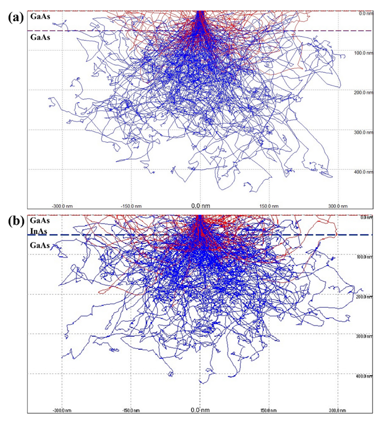
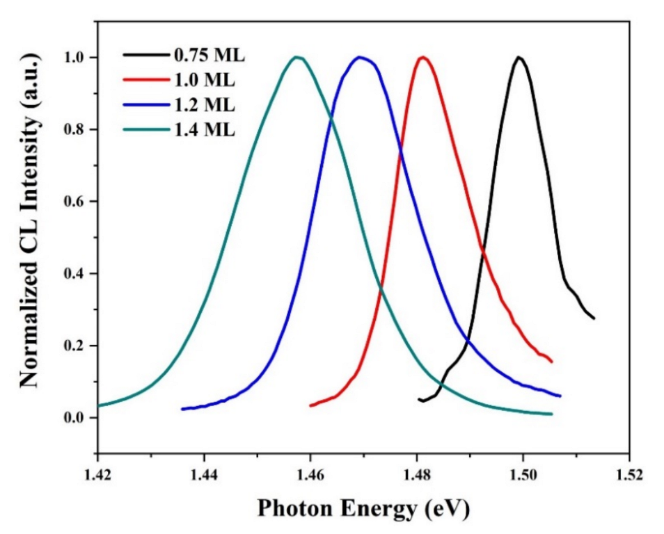
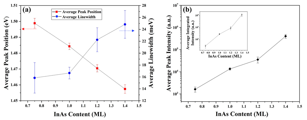
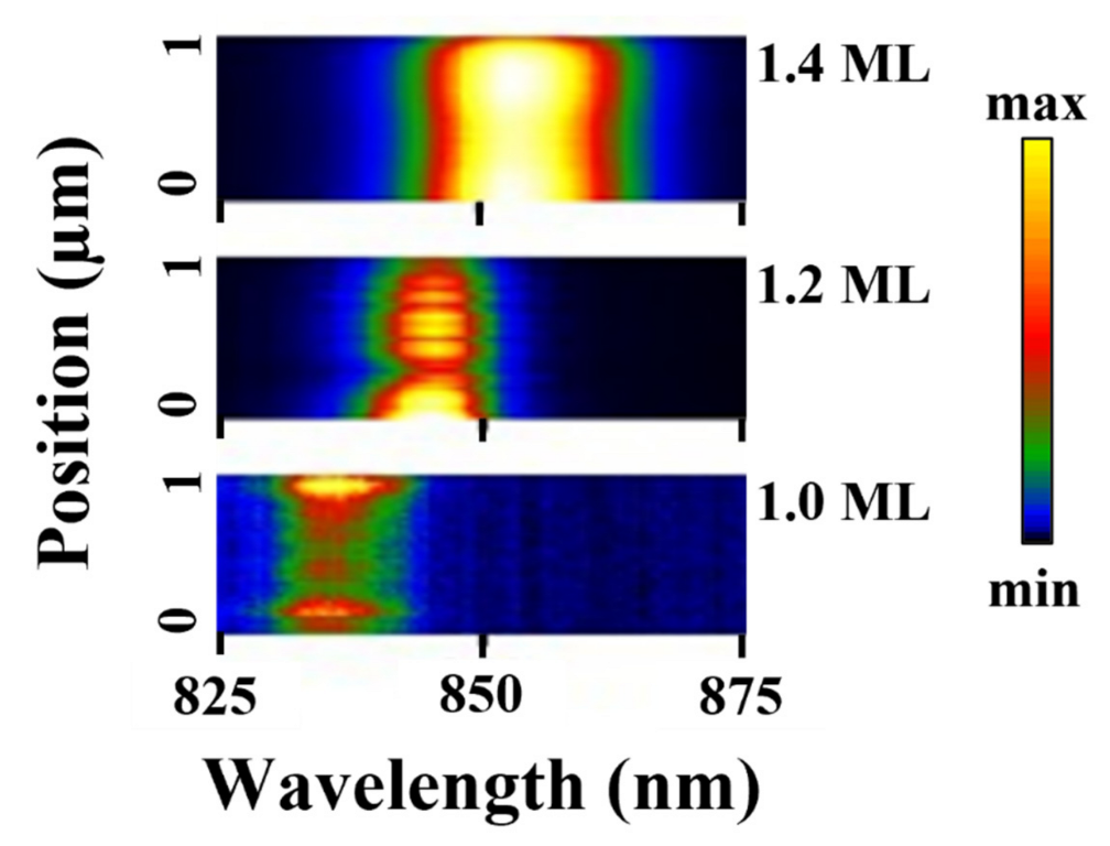
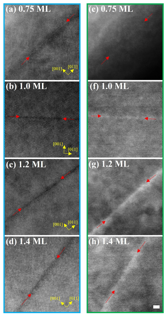
3. Results and Discussion

The structural information and crystallinities of the semiconductor heterostructure are analyzed by X-ray diffraction (XRD) [16]. As presented in Figure 2, besides the GaAs (004) peak, the Pendellösung fringes result from the interference between X-rays scattered from the GaAs layers below the InAs and X-rays from the adjacent GaAs cap layers. Though InAs quantum layers are too thin to be detected, the average coverage of deposited indium is inferred by the dynamical scattering theory simulation [17,18]. The experimental data agree very well with the simulated curves. Meanwhile, once calculated from the curve fitting parameters, the effective thickness of InAs layers and GaAs cap layers are inserted into Figure 2. The intended thickness of InAs based on the growth rate matches with the calculated result. It should be noted that the direct observation of ultrathin layers will be shown later in TEM images. On the other hand, the optical behavior of ultrathin InAs layers should evolve with the structure.
The incident electron beam energy relates to the penetration depth and the interaction volume [19]. Hence, it is crucial to identify a beam energy suitable for this specific heterostructure. To have a stable and comparable CL signal, the electron beam is controlled to scan across a 10 μm × 10 μm square for all measurements, and the normalized CL peak intensities of ultrathin InAs layers from each sample are summarized in Figure 3. Here, the beam energies of 8 keV, 10 keV, 12 keV, and 14 keV have been considered for the excitation. Interestingly, the highest CL peak intensities of 4 distinct InAs layers are found simultaneously at 10 keV, which have been normalized to one. Other data points are calculated proportionally based on the corresponding value at 10 keV. As the beam energy increases beyond 10 keV, the relative CL peak intensities decrease almost linearly with the increasing incident energy. For an incident energy higher than the critical energy (10 keV), electrons have enough energy to penetrate to a deeper area. Therefore, the material below the InAs layer is more likely to be excited, and the relative CL peak intensity of InAs nanostructures shrinks. On the other hand, though the CL peak intensities are still lower than the one excited at the critical energy, an obvious divergence has been observed at the incident energy of 8 keV. In this case, the relative CL peak intensity decreases dramatically as the deposition of InAs decreases. For the same incident energy, a similar number of excitons are generated due to the inelastic collision [20]. Consequently, samples with a higher InAs coverage capture more carriers due to the larger capture cross-section and deeper ground state [15]. This effect is not clear at higher incident energies because excess excitons are created by higher incident beam energies. As a result, the beam energy of 10 keV has been selected for future characterizations.
To reveal the interaction process inside the sample, simulated trajectories of backscattered electrons (BSEs) and secondary electrons (SEs) are shown in Figure 4. Excited by the beam of 10 keV, two models are applied for comparison, including the samples with and without the 1.0 ML InAs layer. BSEs are part of the incident electrons that escape through the sample surface without exciting the quantum layer. On the other hand, SEs are generated after losing energy; more free electrons will be formed exponentially due to inelastic collisions. The energy of free electrons must be low enough, in the order of eV, to excite an electron from the valence band to the conduction band. Excess carriers generated in the GaAs close to InAs nanostructures will be attracted into the quantum well. For both Figure 4a,b, though the incident beam diameter is about 5–10 nm [12], the beam broadening happens inside the material. The radius of the interaction volume reaches 200–300 nm. After inserting an ultrathin InAs layer, the interaction volume only has a negligible change.
Taking advantage of the superior resolution of the focused electron beam, more optical properties of ultrathin InAs nanostructures are investigated by CL spectra [21]. Normalized CL emission peaks of InAs layers, from 0.75 ML to 1.4 ML, are demonstrated in Figure 5. For the characterization of these curves, samples were excited by the beam of 10 keV at discrete points. The main reason for forming those CL peaks is the InAs heavy hole excitation [7]. Generally, the CL emission energy decreases as the deposition of InAs increases. On the contrary, the full width at half maximum (FWHM) is in direct proportion to the content of InAs. One explanation of the CL peak broadening is the lateral confinement of carriers based on the randomly-formed InAs islands or segregations [7]. Another possible reason is the spreading of wavefunctions across multiple InAs nanostructures [17]. Furthermore, the statistical results from ten measurements on key parameters are presented in Figure 6. Individual excitation spots are separated at least 10 μm away from each other to avoid interactions between close InAs nanostructures. The approximate linear behaviors of the average CL emission energy and FWHM as a function of InAs content are obtained in Figure 6a. The gradual redshift of InAs peak positions relates to the lateral confinement or coupling between adjacent nanostructures when the average structural size expands for higher InAs coverage [22,23,24]. Meanwhile, when a higher InAs content is applied, the broadening of linewidth may be caused by the increase of interface roughness or the development of the diversity in structural size and geometry [24,25,26]. In Figure 6b, both average CL peak intensities and integrated intensities exhibit similar roughly linear increases with the InAs deposition, from 0.75 ML to 1.4 ML. This evidence further confirms that a larger average size of InAs nanostructures coexist at a higher ML InAs sample, thereby leading to deeper ground states and larger capture cross-sections [15]. Therefore, a higher CL emission intensity can be obtained with the increase of InAs content. Moreover, since the ground state is deeper, the energy difference between energy levels in the conduction band and valence band of the quantum structure is smaller. Based on the perturbation theory, the transition probability increases for higher ML InAs samples.
Previously, caused by the change of InAs nanostructures, such as islands or segregations, it was found that the optical property varies with the excitation area. To further investigate the space dependence of the CL emission from ultrathin InAs layers, CL line scan profiles [27] are indicated in Figure 7. The electron beam is controlled to scan along a 1.0 μm line on the surface with a 50 nm step size. Therefore, one spectrum image is integrated from 20 CL spectra, and the color corresponds to the intensity of CL emission. Due to the strong charging effect and the weak CL emission at the quick line scan mode, the result from the 0.75 ML InAs layer is not clear. However, obvious discontinuities of CL emissions can be observed from the profiles of the 1.0 ML and 1.2 ML samples. For the 1.4 ML sample, based on a high carrier capture efficiency, though the CL emission is the strongest, two separated hot spots can still be identified.
To have a better knowledge of ultrathin InAs layers, high resolution TEM (HRTEM) images (in the blue box) of all samples are provided in Figure 8a–d. For the 0.75 ML sample, nanostructures are not clear in Figure 8a. As indicated by red arrows in Figure 8b,a line composed of a single atomic layer is observed from the 1.0 ML sample. As shown in Figure 8c,d, structures with two or more atomic layers exist and are caused by the increase of InAs coverage. Moreover, scanning TEM (STEM) images (in the green box) are presented in Figure 8e–h. Though STEM images sacrifice the spatial resolution, a better contrast can be obtained from STEM images. The InAs layer can hardly be seen from the 0.75 ML sample in Figure 8e, while a line of InAs structure appears for the 1.0 ML sample in Figure 8f. Similarly, for the 1.2 and 1.4 ML samples, layers with a higher thickness and roughness are observed. The evolution of ultrathin InAs layers with an increasing InAs content suggests the possibility of the existence of islands or segregations.

4. Conclusions

To conclude, we have investigated the structural and optical properties of sub-monolayer ultrathin InAs nanostructures grown on GaAs by MBE. Although the InAs content only has a tiny change, the XRD and TEM results reveal obvious evolutions on the crystallinity and structure among different ML InAs (from 0.75 to 1.4 ML) samples. It is possible that nanostructures, such as islands or segregations, exist on these ultrathin InAs layers. Corresponding to the changes in structural size, the geometry or roughness, optical behaviors, and carrier capture cross-sections are impacted by the InAs coverage. Compared to the conventional characterization techniques, CL measurements obtain an outstanding spatial resolution based on the electron-beam excitation. Therefore, the CL emission also indicates the evolution on optical properties of InAs nanostructures on different sub-monolayer samples. Further improvements are needed to confirm the physical properties at different growth periods; however, this research provides an applicable method to investigate ultrathin materials.

Author Contributions

Conceptualization, Q.Y. and B.L.; methodology, K.S.; software, K.S. and X.G.; validation, X.G., S.W. and L.H.; formal analysis, Q.Y.; investigation, Q.Y.; resources, Q.Y.; data curation, S.W.; writing—original draft preparation, Q.Y., S.W. and K.S.; writing—review and editing, X.G. and L.H.; visualization, L.H.; supervision, B.L.; project administration, Q.Y.; funding acquisition, Q.Y. All authors have read and agreed to the published version of the manuscript.

Funding

This research was funded by the Natural Science Foundation of Hebei Province (No. A2022104002), the Science and Technology Project of Hebei Education Department (No. BJK2022065), and the Foundation of Transformation and Development Projects of Baoding University (No. 2021Z03).

Data Availability Statement

Not applicable.

Acknowledgments

The authors would like to acknowledge the Institute for Nanoscience and Engineering, University of Arkansas, USA, for the support and guidance.

Conflicts of Interest

The authors declare no conflict of interest.

References

  1. Brübach, J.; Silov, A.; Haverkort, J.; Van Der Vleuten, W.; Wolter, J. Coupled ultrathin InAs layers in GaAs as a tool for the determination of band offsets. Superlattices Microstruct. 1997, 21, 527–532. [Google Scholar] [CrossRef]
  2. Kim, J.O.; Sengupta, S.; Barve, A.V.; Sharma, Y.D.; Adhikary, S.; Lee, S.J.; Noh, S.K.; Allen, M.S.; Allen, J.W.; Chakrabarti, S.; et al. Multi-stack InAs/InGaAs sub-monolayer quantum dots infrared photodetectors. Appl. Phys. Lett. 2013, 102, 011131. [Google Scholar] [CrossRef]
  3. Beattie, N.S.; See, P.; Zoppi, G.; Ushasree, P.M.; Duchamp, M.; Farrer, I.; Ritchie, D.A.; Tomić, S. Quantum Engineering of InAs/GaAs Quantum Dot Based Intermediate Band Solar Cells. ACS Photonics 2017, 4, 2745–2750. [Google Scholar] [CrossRef]
  4. Iotti, R.C.; Andreani, L.C.; Di Ventra, M. Tight-binding approach to excitons bound to monolayer impurity planes: Strong radiative properties of InAs in GaAs. Phys. Rev. B 1998, 57, R15072–R15075. [Google Scholar] [CrossRef]
  5. Goñi, A.R.; Stroh, M.; Thomsen, C.; Heinrichsdorff, F.; Türck, V.; Krost, A.; Bimberg, D. High-gain excitonic lasing from a single InAs monolayer in bulk GaAs. Appl. Phys. Lett. 1998, 72, 1433–1435. [Google Scholar] [CrossRef]
  6. Baskaran, A.; Smereka, P. Mechanisms of Stranski-Krastanov growth. J. Appl. Phys. 2012, 111, 044321. [Google Scholar] [CrossRef]
  7. Kumar, R.; Maidaniuk, Y.; Kuchuk, A.; Saha, S.K.; Ghosh, P.K.; Mazur, Y.I.; Ware, M.E.; Salamo, G.J. Excitation intensity and thickness dependent emission mechanism from an ultrathin InAs layer in GaAs matrix. J. Appl. Phys. 2018, 124, 235303. [Google Scholar] [CrossRef]
  8. Belousov, M.V.; Ledentsov, N.N.; Maximov, M.V.; Wang, P.D.; Yasievich, I.N.; Faleev, N.N.; Kozin, I.A.; Ustinov, V.M.; Kop’ev, P.S.; Torres, C.M.S. Energy levels and exciton oscillator strength in submonolayer InAs-GaAs heterostructures. Phys. Rev. B 1995, 51, 14346–14351. [Google Scholar] [CrossRef]
  9. Wang, P.D.; Ledentsov, N.N.; Torres, C.M.S.; Yassievich, I.N.; Pakhomov, A.; Egovov, A.Y.; Kop’ev, P.S.; Ustinov, V.M. Magneto-optical properties in ultrathin InAs-GaAs quantum wells. Phys. Rev. B 1994, 50, 1604–1610. [Google Scholar] [CrossRef]
  10. Krestnikov, I.; Ledentsov, N.; Hoffmann, A.; Bimberg, D. Arrays of Two-Dimensional Islands Formed by Submonolayer Insertions: Growth, Properties, Devices. Phys. Status Solidi 2001, 183, 207–233. [Google Scholar] [CrossRef]
  11. Stöger-Pollach, M.; Pichler, C.F.; Dan, T.; Zickler, G.A.; Bukvišová, K.; Eibl, O.; Brandstätter, F. Coherent light emission in cathodoluminescence when using GaAs in a scanning (transmission) electron microscope. Ultramicroscopy 2021, 224, 113260. [Google Scholar] [CrossRef] [PubMed]
  12. Hofmann, C.E.; Vesseur, E.J.R.; Sweatlock, L.A.; Lezec, H.J.; de Abajo, F.J.G.; Polman, A.; Atwater, H.A. Plasmonic Modes of Annular Nanoresonators Imaged by Spectrally Resolved Cathodoluminescence. Nano Lett. 2007, 7, 3612–3617. [Google Scholar] [CrossRef] [PubMed]
  13. Yan, Q.; Li, X.; Liang, B. Plasmonic Emission of Bullseye Nanoemitters on Bi2Te3 Nanoflakes. Materials 2020, 13, 1531. [Google Scholar] [CrossRef] [PubMed]
  14. Reszka, A.; Wierzbicka, A.; Sobczak, K.; Jahn, U.; Zeimer, U.; Kuchuk, A.V.; Pieniążek, A.; Sobanska, M.; Klosek, K.; Zytkiewicz, Z.R.; et al. An influence of the local strain on cathodoluminescence of GaN/AlxGa1−xN nanowire structures. J. Appl. Phys. 2016, 120, 194304. [Google Scholar] [CrossRef]
  15. Wang, Y.; Sheng, X.; Guo, Q.; Li, X.; Wang, S.; Fu, G.; Mazur, Y.I.; Maidaniuk, Y.; Ware, M.E.; Salamo, G.J.; et al. Photoluminescence Study of the Interface Fluctuation Effect for InGaAs/InAlAs/InP Single Quantum Well with Different Thickness. Nanoscale Res. Lett. 2017, 12, 229. [Google Scholar] [CrossRef]
  16. Brandt, O.; Tapfer, L.; Cingolani, R.; Ploog, K.; Hohenstein, M.; Phillipp, F. Structural and optical properties of (100) InAs single-monolayer quantum wells in bulklike GaAs grown by molecular-beam epitaxy. Phys. Rev. B 1990, 41, 12599–12606. [Google Scholar] [CrossRef]
  17. Tran, C.A.; Ares, R.A.; Karasyuk, V.A.; Watkins, S.P.; Letourneau, G.; Leonelli, R. Origin of sharp lines in photoluminescence emission from submonolayers of InAs in GaAs. Phys. Rev. B 1997, 55, 4633–4638. [Google Scholar] [CrossRef]
  18. Giannini, C.; Tapfer, L.; Lagomarsino, S.; Boulliard, J.C.; Taccoen, A.; Capelle, B.; Ilg, M.; Brandt, O.; Ploog, K.H. X-ray standing wave and high-resolution x-ray diffraction study of the GaAs/InAs/GaAs(100) heterointerface. Phys. Rev. B 1993, 48, 11496–11499. [Google Scholar] [CrossRef]
  19. Grünbaum, E.; Napchan, E.; Barkay, Z.; Barnham, K.; Nelson, J.; Foxon, C.T.; Roberts, J.S.; Holt, D.B. Evaluation of the minority carrier diffusion length by means of electron beam induced current and Monte Carlo simulation in AlGaAs and GaAs p-i-n solar cells. Semicond. Sci. Technol. 1995, 10, 627–633. [Google Scholar] [CrossRef]
  20. Klein, C.A. Bandgap Dependence and Related Features of Radiation Ionization Energies in Semiconductors. J. Appl. Phys. 1968, 39, 2029–2038. [Google Scholar] [CrossRef]
  21. Su, P.-Y.; Liu, H.; Kawabata, R.M.S.; Weiner, E.C.; Jakomin, R.; Pires, M.P.; King, R.R.; Souza, P.L.; Ponce, F.A. Effect of InAs quantum dots capped with GaAs on atomic-scale ordering in Ga0.5In0.5P. J. Appl. Phys. 2019, 125, 053104. [Google Scholar] [CrossRef]
  22. Selvidge, J.; Norman, J.; Salmon, M.E.; Hughes, E.T.; Bowers, J.E.; Herrick, R.; Mukherjee, K. Non-radiative recombination at dislocations in InAs quantum dots grown on silicon. Appl. Phys. Lett. 2019, 115, 131102. [Google Scholar] [CrossRef]
  23. Yuan, Z.L.; Xu, Z.Y.; Zheng, B.Z.; Xu, J.Z.; Li, S.S.; Ge, W.; Wang, Y.; Wang, J.; Chang, L.L.; Wang, P.D.; et al. Two-dimensional excitonic emission in InAs submonolayers. Phys. Rev. B 1996, 54, 16919–16924. [Google Scholar] [CrossRef]
  24. Patanè, A.; Polimeni, A.; Capizzi, M.; Martelli, F. Linewidth analysis of the photoluminescence of InxGa1−xAs/GaAs quantum wells (x = 0.09, 0.18, 1.0). Phys. Rev. B 1995, 52, 2784–2788. [Google Scholar] [CrossRef]
  25. Jiang, Q.; Wang, G.-C. Scaling of island size distribution and island coalescence in monolayer epitaxial growth of 1 × 1 films. Surf. Sci. 1995, 324, 357–364. [Google Scholar] [CrossRef]
  26. Mukherjee, K.; Selvidge, J.; Jung, D.; Norman, J.; Taylor, A.A.; Salmon, M.; Liu, A.Y.; Bowers, J.E.; Herrick, R.W. Recombination-enhanced dislocation climb in InAs quantum dot lasers on silicon. J. Appl. Phys. 2020, 128, 025703. [Google Scholar] [CrossRef]
  27. Rodt, S.; Reitzenstein, S. High-performance deterministic in situ electron-beam lithography enabled by cathodoluminescence spectroscopy. Nano Express 2021, 2, 014007. [Google Scholar] [CrossRef]
Figure 1. (a) Schematic of the sample structure from the cross-section view. (b) Schematic of the CL setup.
Crystals 12 01225 g001
Figure 2. Experimental and simulated XRD patterns of all samples for the symmetrical (004) plane. The inserted table indicates the calculated thickness of ultrathin InAs layers and GaAs cap layers.
Crystals 12 01225 g002
Figure 3. Normalized peak intensities of different InAs layers extracted from corresponding CL spectra excited with different beam energy. To indicate the relative trend, the highest intensities have been normalized to one.
Crystals 12 01225 g003
Figure 4. Cross-sectional images of simulated trajectories of backscattered electrons (red) and secondary electrons (blue) in samples (a) without any InAs and (b) with a 1.0 ML InAs layer. The incident energy of electrons is selected to be 10 keV.
Crystals 12 01225 g004
Figure 5. Normalized CL emission peaks of ultrathin quantum structures with 0.75 ML, 1.0 ML, 1.2 ML, and 1.4 ML InAs layers, respectively. All CL spectra are acquired with an identical beam energy of 10 keV at 80 K.
Crystals 12 01225 g005
Figure 6. (a) Average peak position and linewidth of different InAs layers with a function of InAs content. (b) Average peak intensity and integrated intensity of different InAs layers with a function of InAs content. The statistical result is obtained from ten distinct excitation spots far away from each other.
Crystals 12 01225 g006
Figure 7. CL spectrum images of samples with 1.0 ML, 1.2 ML, and 1.4 ML InAs layers, respectively. All results are obtained by scanning the beam alone a line of 1 μm. The step size is 50 nm.
Crystals 12 01225 g007
Figure 8. (ad) HRTEM images of four samples with different amounts of InAs. (eh) STEM images of relative samples with different InAs content. The InAs structures are indicated by red arrows, and the scale bar corresponds to 2 nm.
Crystals 12 01225 g008
Publisher’s Note: MDPI stays neutral with regard to jurisdictional claims in published maps and institutional affiliations.

