1. Introduction
Superjunction (SJ) was introduced to improve the ’compromise’ relation of a traditional MOSFET [
1,
2]. SJ MOSFET creates n/p pillars with the same doping concentrations in the drift region, which could significantly decrease the on-resistance, while the device breakdown voltage (V
) remains the same. The phenomenon is due to the lateral loss of the SJ MOSFET drift region carrier [
3]. However, SJ MOSFET will make the parasitic diodes turn on due to fast reverse recovery, further causing severe oscillation in the reverse recovery of the device, and having an adverse effect on the circuit [
4,
5,
6]. Recently, a vertical SJ MOSFET with n-Si and p-3C-SiC pillars was proposed, which can weaken the sensitivity of BV to charge imbalances and improve the reverse recovery [
7,
8].
Some groups reported several innovative structures, such as integrating isolated transverse NMOS into the P-body region of SJ devices in order to effectively suppress the conduction of the SJ-VDMOS intrinsic diode and eliminate the hole current in the voltage maintenance layer during the continuation [
9]. Weifeng Sun proposed a new device structure by introducing an oxide pillar to separate the n-pillar and p-pillar, which attained a Schottky diode between the source contact at the top of the p-pillar and p-base. The hole carrier of the p-pillar injected in the reverse state was significantly reduced, resulting in the corresponding reduction of the hole density in the drift region [
10]. J. Kim and K. Kim presented a novel 4H-SiC super junction UMOSFET with a heterojunction diode and the research was carried out by numerical simulations [
11]. Herein, we introduced a Schottky barrier diode(SBD) on the source contact at the top of the n-Si pillar to further improve the device’s reverse recovery performance.
In this work, a Schottky barrier diode (SBD) with different work functions was integrated to improve reverse recovery performance by changing the carrier extraction path inside the device. TCAD Silvaco simulated the theory of SJ with several parameter utilizations, such as concentration, thickness, and so on. The performance of the device was exhibited, such as reverse recovery time and breakdown voltage. Additionally, the effects of different metal work functions, temperature, and the lifetimes of minority carriers to the device were also explored. It is convincing that the Si/SiC SJ with SBD could effectively increase the switching speed and reduce the switching losses in high-speed switching circuits.
2. Device Structure and Mechanism
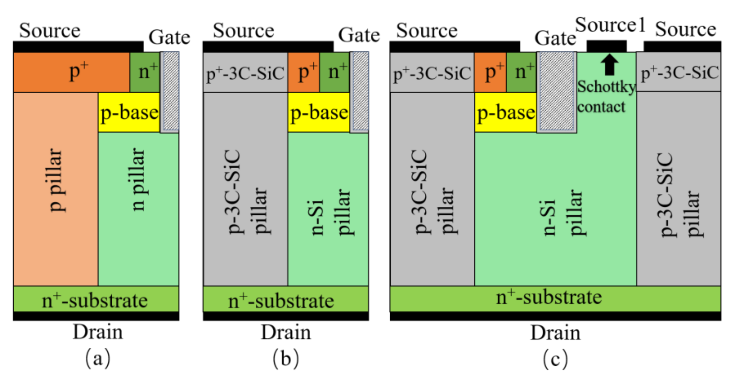
The cross-sectional structures of the conventional Si SJ MOSFET (Si SJ), SJ MOSFET with n-Si and p-3C-SiC Pillars (Si/SiC SJ), as well as the proposed SJ MOSFET with SBD (Si/SiC SJ with SBD) are shown in
Figure 1. The Si/SiC SJ with SBD is distinguished from the Si/SiC SJ by integrating a parallel SBD. In the reverse conduction state, the SBD is forward-biased, pulling electrons from the drift region and leading most of the current flows out from the SBD. Consequently, the total current of SJ MOSFET is significantly reduced, resulting in a shorter reverse recovery time (t
) and lower Q
. The device simulation and the mix-mode simulation results were obtained using Silvaco TCAD. The superjunction MOSFET was structured by using uniformly alternating P-pillars and N-pillars instead of the N-region in a conventional MOSFET to act as the drift region of the device; the device cell is shown in
Figure 1c. During forwarding turn-on, the lateral PN junction between the P-pillar and N-pillar is in a positive bias state, and the carriers inside both the P-pillar and N-pillar are involved in conducting. When the device is turned off, the transverse electric field between the P-pillar and N-pillar will deplete the carriers inside the body transversely, making the non-equilibrium carriers inside the device in a point and equilibrium state. Although the doping concentration is several orders of magnitude higher, the carrier concentration at the device’s withstand voltage is not much different from that of the intrinsic semiconductor. The structure designed in this chapter was placed on the DUT of the test circuit, and the constant voltage source supplying the whole circuit at both ends of the circuit was set to 300 V. The constant current source was set so that the current flowing through the device under the test was 20 A and the di/dt rate at the turn-off was 200 A/
s to test the reverse recovery characteristics of the device. It was also necessary to choose suitable models and contact metal work functions. Finally, TonyPlot was utilized to attain mixed-mode simulation results.
3. Results and Discussions
The parameters of SJ MOSFET (determined according to the theory of SJ [
3]) are listed in
Table 1.
Table 1 shows the comparisons with other recently published PGA. According to the charge compensation principle, the n/p pillars can use a high-doping concentration to obtain a low specific on-resistance (R
) with a high breakdown voltage (V
). To explore the influence of the introduction of the new SBD structure, we set the other parameters the same among the three structures, such as the concentrations of the n/p pillar, n
-source concentration, p
-source concentration, n
-substrate concentration (N
), and p-base concentration (N
).
Figure 2a shows the forward breakdown voltage curves for Si/SiC SJ and Si/SiC SJ with SBD at the turn-off state. SBD integration did not affect the breakdown voltage, while the off-state leakage of the device increased slightly. The breakdown simulation curves of the Schottky contact with different metal work functions are shown in
Figure 2b. As the metal work function decreased, the Schottky barrier height declined, leading to more electrons flowing from the SBD into the device and a larger leakage current at the off-state.
Figure 3a shows the reverse recovery characteristics of these three devices. The inset shows the test circuit configuration where the device under test (DUT) had an area of 0.2 cm
, and the current communication rate di/dt was set to 200 A/
s by setting RG = 200
and Conv-SJ-MOSFET (CONV.) as the low-side switch. After integrating an SBD, the t
dropped significantly, and the I
obtained 11.94 A, which decreased by 84.0% for Si SJ (74.76 A) and 74.0% for Si/SiC SJ (11.94 A), while the Q
achieved 0.50
C, which decreased by 90.5% for Si SJ (5.27
C) and 42.3% for Si/SiC SJ (3.04
C), respectively.
Figure 3b shows the voltage curves of these three devices during the reverse recovery. When di/dt was set at 200 A/
s, the oscillation voltage of the Si SJ reached 305.1 V, which is even more significant than the driving voltage at the drain-source side of the device (300 V), consequently posing a hazard to the subsequent circuit reliability. After the introduction of the SBD, the oscillation of the reverse recovery voltage was significantly reduced, and the maximum voltage values (V
) also dropped to 171.6 V, which decreased by 43.7% (Si SJ, 305.1 V A) and 14.8% (Si/SiC SJ, 259.90 V) during the oscillation.
Figure 4a shows the currents of source and source1 during reverse recovery for Si/SiC SJ with SBD and the work function of source1 was 4.8 eV. The reverse recovery characteristics of the MOSFET devices were ultimately due to the parasitic diode that turned on to extract the stored charge when the device was turned off and acted as a flyback diode. As shown in
Figure 4a, at the beginning of the shutdown, the primary current in the Si/SiC SJ with SBD was the multinomial current generated by the source1 conduction. In contrast, the current flowed mainly from the source when the SBD was shut down due to the unidirectional conduction characteristic. Therefore, the parasitic diode in Si/SiC SJ with SBD only extracted a small amount of stored charge in reverse recovery, significantly improving the reverse recovery characteristics.
The reverse recovery curves for different SBD metals (the work function is set at 4.7, 4.8, 4.9 eV) are simulated in
Figure 4b to explore the influence of the Schottky barrier height induced by the different metal work functions. As the work function of the metal decreases from 4.9 to 4.7 eV, more majority carriers will flow out of the SBD. Due to the smaller barrier height, fewer minority carriers will flow out of the parasitic flyback diode. Consequently, it will reduce the Q
and improve the reverse recovery characteristics. As shown in
Figure 4c, compared to the Si/SiC SJ, there is a gap in the switching rate of Si/SiC SJ with SBD. After introducing the SBD, the contact area between the gate and the drift region increased, causing significant increases in the gate capacitance (C
). Due to the increased capacitance of the CGD, the charging and discharging times of the C
were prolonged, extending the device switching-on time. In addition, the gate current was 0.5 A, which is only 3% of the saturation current of 17 A. It does not have a significant impact on device performance.
The reverse recovery curves for different working temperatures (the operating temperatures were set at 300 and 400 K) are simulated in
Figure 5a to explore the influence of the minority carrier mobility in the recovery process. As the working temperature decreases from 400 K to 300 eV, more majority carriers will flow out of the SBD, and fewer minority carriers will flow out of the parasitic flyback diode due to the increase in mobility, further reducing the Q
and correspondingly improving the reverse recovery characteristics. As shown in
Figure 5b, the influence of the minority carrier lifetime (the lifetime was set at 0.1
s, 1
s, and 10
s) is explored. It is evident that, with less minority carrier lifetimes, fewer minority carriers will flow out of the parasitic flyback diode, and they will recombine with the majority carrier more easily. A newly designed structure of Si/SiC SJ with SBD is illustrated in
Figure 5c, and compared to the Si/SiC SJ, and there is a gap in the switching rate of Si/SiC SJ with SBD (
Figure 5d). In the simulation results, the original and improved structure currents achieved the same value, 16.8 A. At the same time, there exists a gap between the transient time—the rising edge differs by 0.09
s, and the falling edge varies by 0.24
s. It is convincing that utilizing this newly designed structure makes sense to decrease the gate capacitance (C
), increase switching speed, and reduce switching losses in high-speed switching circuits.


