Article

Study of Temperature Effects on the Design of Active Region for 808 nm High-Power Semiconductor Laser

1
State Key Laboratory of Transient Optics and Photonics, Xi’an Institute of Optics and Precision Mechanics, Chinese Academy of Sciences, Xi’an 710119, China
2
University of Chinese Academy of Sciences, Beijing 100049, China
*
Author to whom correspondence should be addressed.
Crystals 2023, 13(1), 85; https://doi.org/10.3390/cryst13010085
Submission received: 15 November 2022 / Revised: 16 December 2022 / Accepted: 26 December 2022 / Published: 2 January 2023
(This article belongs to the Special Issue Frontiers of Semiconductor Lasers)

Abstract

:
High-power, broad-area, semiconductor lasers are attractive sources for material processing, aerospace, and laser pumping. The design of the active region is crucial to achieve the required high power and electro-optical conversion efficiency, since the temperature significantly affects the performance of the quantum well, including the internal quantum efficiency and mode gain. In this work, the temperature effects on the active region of a 808 nm high-power semiconductor laser were investigated theoretically and experimentally. The simulations were performed with a Quasi-3D model, which involved complete steady-state semiconductor and carrier confinement efficiency combined with a new mathematical method. The critical aluminum content of the quantum barrier was proposed and the relationship between temperature and various loss sources was disclosed in the temperature range of 213 to 333 K, which provides a reliable reference for the design of epitaxial structures of high-power semiconductor lasers in different operating conditions. Subsequently, the optimized epitaxial structure was determined and used to fabricate standard laser bar chips with a cavity length of 2 mm. The experimental electro-optical conversion efficiency of 71% was demonstrated with a slope efficiency of 1.34 W/A and an injection current of 600 A at the heatsink temperature of 223 K. A record high electro-optical conversion efficiency of 73.5% was reached at the injection current of 400 A, while the carrier confinement efficiency was as high as 98%.

1. Introduction

High-power semiconductor lasers have various excellent characteristics, including high output power and electro-optical conversion efficiency, compact structure, high reliability, long operating lifetime, and simple electric driving conditions, and have thus already been widely applied in material processing, the medical field, communication, aerospace, laser pumping, and so on [1]. In some specific fields, such as communication and aerospace, semiconductor lasers are required to adapt to harsh working conditions, especially drastic temperatures, which will cause the device performance to deteriorate sharply or even fail. Therefore, the temperature characteristic of high-power semiconductor lasers has always been a research hotspot. This paper mainly studies the performance of semiconductor lasers in the temperature range of 213 to 333 K, which is a common requirement for industrial applications [2]. Generally, temperature has significant effects on the properties of semiconductor materials, including mobility [3], energy band structure [4], carrier concentration, and refractive index [5], as well as dynamic processes, including drift-diffusion equations, current injection [6], current distribution [7], and gain-absorption [8], making the temperature analysis of semiconductor lasers rather complicated. From the perspective of the vertical epitaxial structure, temperature affects the active region more significantly than other non-active layers, including internal parameters such as mode gain, injected carrier concentration, carrier leakage, and internal optical absorption loss, which ultimately affect the threshold current, slope efficiency, voltage, and resistance [9]. For this reason, this paper mainly focuses on the design of the active region and analyzes differences in performance in the active region at different temperatures.
There is extensive literature on many aspects of epitaxial design from the perspective of temperature. In 2017, Y. F. Song reported 808 nm semiconductor laser arrays with a 1.5 mm cavity length and conduction cooling package. When the temperature dropped from 298 to 233 K, the electro-optical conversion efficiency increased from 56.7% to 66.8% and the carrier leakage ratio dropped from 16.6% to 3.1%, indicating that the significant reduction in carrier leakage loss was the main reason leading to the increased electro-optical conversion efficiency at low temperature [10]. In 2015, C. Frevert elaborated on the power and voltage characteristics of 9xx nm GaAs-based semiconductor lasers in the temperature range of 208 to 298 K, showing the ratio of quantum barrier height to temperature, Δ E / ( k B T ) , had a remarkable effect on the differential internal quantum efficiency. These results showed that the carrier leakage was significantly affected by temperature when Δ E / ( k B T ) was less than seven [11]. In 2017, K. H. Hasler conducted low-temperature research on 9xx nm GaAs-based high-power semiconductor lasers and analyzed the quantum barrier and waveguide at 200 and 300 K for AlGaAs materials with different aluminum (Al) contents. The results indicated that the increase in the mode gain of the active region and the decrease in the accumulation of free electrons in the P-waveguide layer at a low temperature of 200 K led to a decrease in the threshold current and an increase in the slope efficiency, thereby increasing the power and electro-optical conversion efficiency [12]. In 2019, M. P. Wang studied the output power, electro-optical conversion efficiency, and spectral variation of high-power semiconductor lasers in the temperature range of 213 to 273 K. The results showed that the energy distribution of injected carriers became narrower at low temperatures, so the leakage of carriers was reduced. Coupled with the decrease in the transparent carrier concentration and internal optical loss, the threshold current eventually decreased as the temperature dropped [13].
Although temperature characteristics research of high-power semiconductor lasers is relatively intensive, few studies have been able to match theory and experiment perfectly. For one thing, studies only utilized experimental methods to obtain output data and qualitatively describe related internal physical quantities. However, lasers designed for a specific temperature scope are not always suitable for all other temperature ranges. Therefore, the variable temperature-dependent experimental test with a fixed structure did not reflect the best performance of the device, reducing the practicality of the experimental data. For another, the related theoretical analysis of internal quantum efficiency, η i , and material gain, g 0 , is less reported. There is no distinct explanation describing how carrier leakage loss is affected by temperature and barrier height, or how the gain of the active region changes with temperature and materials, which is inconvenient to the design of the active region at a specific temperature.
In this work, the epitaxial structure of the 808 nm GaAs-based semiconductor laser was optimized in detail. The active region consisted of a commonly used InAlGaAs/AlGaAs strained quantum well, and the other epitaxial layers were based on an asymmetric, wide waveguide structure [14]. The trends of η i and g 0 were theoretically investigated in the scope of the active region. To simplify the calculation of η i , a mathematical model to calculate the specific amount of carrier leakage in quantum wells was uniquely proposed and its approximate expression and application scope were derived, which was simple, time-saving, and accurate. Together with simulation tools, this model can make accurate judgments on the output performance of semiconductor lasers at different temperatures.
In Section 2, the mathematical model for internal quantum efficiency and mode gain was derived, and then temperature dependence was preliminarily analyzed. Section 3 is devoted first to the introduction of the simulation tools and then to the summary of the most relevant physical effects of the model. In Section 4, the mathematical model of Section 2 was embedded in the simulation tools of Section 3 to analyze the temperature effects. In Section 5, the simulated results are compared with the experimental data to verify the correctness of analysis in Section 4. The paper ends with a conclusion in Section 6.

2. Theory

The core output performance of a semiconductor laser is the output power, P o u t , and its empirical equation is [15]:
P o u t = η s l o p ( I I t h ) = h c q λ η i α m α i + α m e x p ( Δ T T 1 ) [ I W L J t r η i e x p ( α i + α m Γ g 0 ) e x p ( Δ T T 0 ) ]
where
ηslop
is the slope efficiency;
Ith
  is the threshold current;
h 
    is the Planck’s constant;
c 
    is the speed of light in vacuum;
q 
    is the amount of elementary charge;
λ 
    is the lasing wavelength;
ηi 
   is the internal quantum efficiency;
αm 
  is the mirror loss, and α i is the internal optical loss;
ΔT
   is the temperature rise of the active region relative to the heatsink;
T0
    and T 1 are the characteristic temperatures that depict the temperature sensitivity of threshold current and slope efficiency, respectively;
L 
    is the length of the resonant cavity, and W is the width of the device electrode;
Jtr 
   is the transparent current density;
Γg0
  is the mode gain, which is the product of the optical confinement factor   Γ in the quantum well and the material gain g 0 .
According to Equation (1), it is essential to reduce the threshold current and increase the slope efficiency as much as possible to increase the output power. Generally, the state of the active region has the most significant influence on these two parameters. Therefore, the relationships among the internal quantum efficiency η i , the material gain g 0 and the temperature T are derived as follows based on the theory of semiconductor lasers.
The internal quantum efficiency is defined as the ratio of the number of photons generated in the active region to the electron-hole pairs injected from the electrode. Due to the existence of impurity defects in the active region, the heterojunction interface state, the carrier leakage in the quantum well, etc., the electron-hole pairs injected into the active region cannot produce 100% radiative recombination, so η i is always less than 1. According to the reasons for the loss in carrier utilization, the internal quantum efficiency can be divided into three parts, as follows:
η i = η i n j η c o n η r a d
where η i n j is the ratio of the carriers injected into the active area to those injected from the electrode, which is assumed as 1 in this paper [6].
η c o n is defined as the proportion of carriers injected into the active region that is effectively confined in the quantum well. This part of loss is mainly caused by the insufficient height of the quantum barrier and the excessively high temperature of the active region, causing the carriers to cross over the barrier into the waveguide layer. Therefore, it is critical to study the barrier height of the active region at different ambient temperatures to improve internal quantum efficiency.
η r a d   is the ratio of the number of photons generated by effective radiation recombination to the number of carriers confined in the quantum well [16].
Next, the new carrier confinement efficiency model is derived. The electron concentration in the energy range from the bottom of the conduction band E c in the quantum well to any higher energy level E is:
n ( E ) = E c E g c ( E ) f ( E ) d E
Similarly, the hole concentration in the energy range from the bottom of the valence band E v in the quantum well to any lower energy level E is:
p ( E ) = E v E g v ( E ) [ 1 f ( E ) ] d E
where g c ( E ) and g v ( E ) are the state density of the conduction band and valence band, respectively. f ( E ) is the Fermi-Dirac distribution function. The leakage of carriers in the quantum well originates from the part over the quantum barrier height [17]. Therefore, η c o n is approximately equal to the ratio of the carriers confined in the potential well Δ E c and Δ E v to the carrier concentration over the whole energy band:
η c o n = n ( E c , b a r r i e r ) + p ( E v , b a r r i e r ) n ( ) + p ( ) = E c , w e l l E c , b a r r i e r g c ( E ) f ( E ) d E + E v , w e l l E v , b a r r i e r g v ( E ) [ 1 f ( E ) ] d E E c , w e l l g c ( E ) f ( E ) d E + E v , w e l l g v ( E ) [ 1 f ( E ) ] d E e x 1 e x 2 e x 1
where E c , b a r r i e r and E v , b a r r i e r are the bottom of the conduction band and valence band in the quantum barrier, respectively, and the position of the Fermi energy level is crucial to the accuracy of the model, which is extrapolated by the simulation tools.
The first-order approximation of the model was derived when ignoring the hole confinement and the higher subband in the quantum well, as well as approximating the Fermi distribution function as a Boltzmann distribution. This is shown in the second line of Equation (5), where x 1 = E i 1 + E c E F k B T , x 2 = Δ E c + E c E F k B T . E i 1 is the energy difference between the first electron subband and the conduction band bottom of the quantum well, Δ E c is the energy difference between the conduction band bottom of the quantum well and the quantum barrier, and k B is the Boltzmann constant.
It can be deduced that the carrier confinement efficiency is mainly affected by the barrier height ( Δ E c and Δ E v ), the active region temperature T, and the injected current density J (affecting the position of the Fermi energy level). As for the AlGaAs quantum barrier, the larger the Al content, the higher the Δ E c and Δ E v , and thus, the better the carriers are confined. However, high Al content will cause the resistance to increase, resulting in lower electro-optical conversion efficiency. Thus, for different operating temperatures, choosing a suitable Al content for the barrier layers can maximize the power and electro-optical conversion efficiency of the semiconductor laser.
In terms of the material gain in the quantum well, the gain spectrum equation is as follows [15]:
g ( ω ) = n , m g m a x [ f c n ( E t = ω E h m e n ) f v m ( E t = ω E h m e n ) ] H ( ω E h m e n )
where g m a x is the peak gain and   H ( ω E h m e n ) represents the unit step function. The occupation probability of electrons in the nth conduction subband and the mth hole subband are shown as follows, respectively [15],
f c n ( E t = ω E h m e n ) = 1 1 + e [ E e n + ( m r * / m e * ) ( ω E h m e n ) F c ] / k B T
f v m ( E t = ω E h m e n ) = 1 1 + e [ E h m ( m r * / m h * ) ( ω E h m e n ) F v ] / k B T
When f c n > f v m , population inversion is achieved, and the net gain will be generated. According to Equation (6), the active region temperature T mainly affects the energy distribution states f c n and f v m of the injected carriers, thereby changing the gain peak. Simultaneously, the temperature also causes the quantum well subband transition energy E h m e n to change and then shifts the peak wavelength.

3. Simulation Model and Epitaxial Parameters

The simulation tools we applied were exploited to analyze the performance of different types of semiconductor devices, such as F-P lasers [18], tapered semiconductor optical amplifiers (SOA) [19], VCSELs [20], and LEDs [21], where it has demonstrated predictive capabilities. In brief, the program self-consistently solves the complete steady-state electrical, optical, and thermal equations for customers. The simulators included Maxwell’s wave equation solver for the normal modes in the waveguide; the 3D electrical solver of Poisson and continuity equations; the energy band structure solver with strain effect, quantum effect, and band-mixing effect; and the 3D thermal solver of heat-flow equation. Table 1 summarizes the basic physical effects included in the simulations and their dependence on temperature, carrier concentration, and wavelength.
The elaborate epitaxial structure we applied to analyze the temperature effects was based on our original epitaxial structure, as shown in Table 2. The quantum well thickness was selected to be 8 nm with a compressed strain of approximately 1%, and the quantum barrier thickness was fixed to 50 nm. The Al content of the barrier ranged from 0.1 to 0.35, which needed to be optimized through the temperature analysis. The simulated temperature ranged from 213 to 363 K, which was divided into 16 groups with the same gap. The chip of cm-bar contained 44 emitting units, each with a 170 μm electrode width, a 2 mm cavity length, and a front and rear reflectivity of 3% and 91.5%, respectively. Only the single-emitting unit of laser bars needed to be simulated due to the consistency of the epitaxial structure.

4. Simulation Results and Discussion

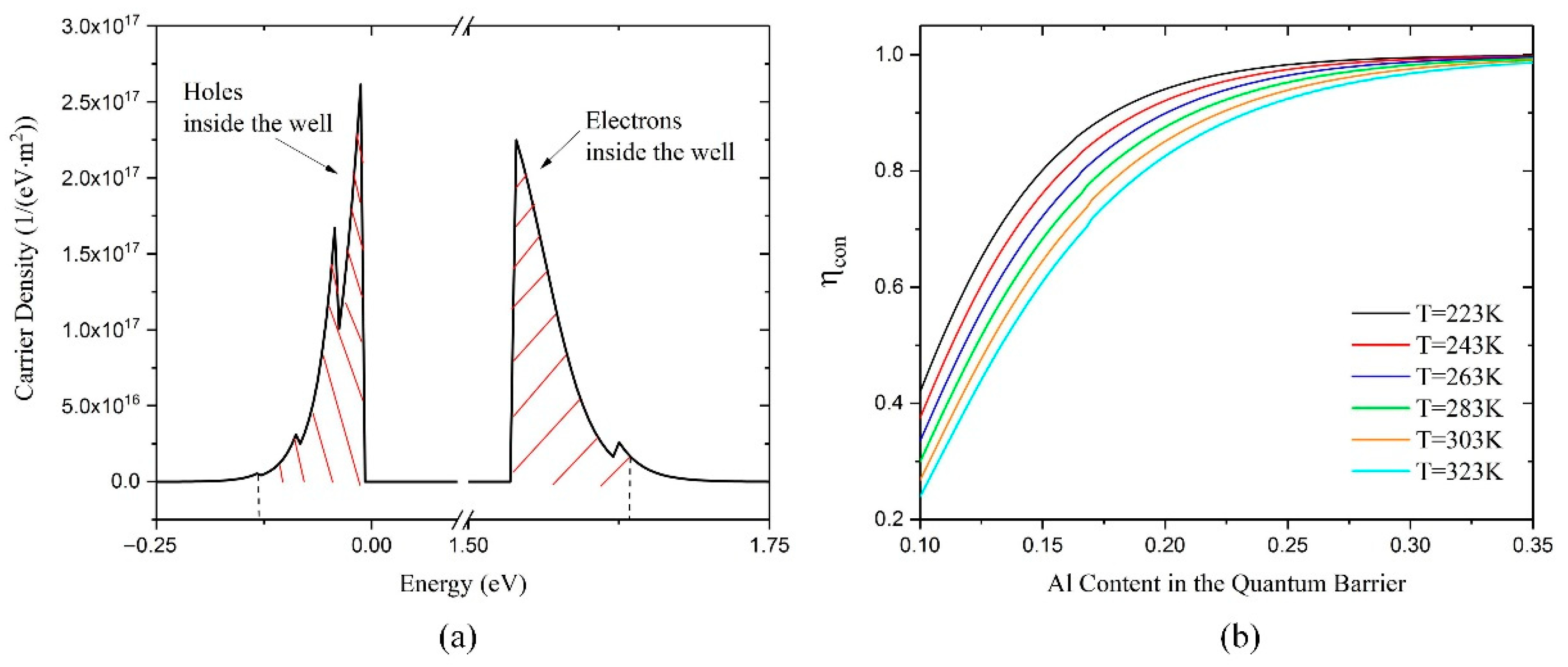
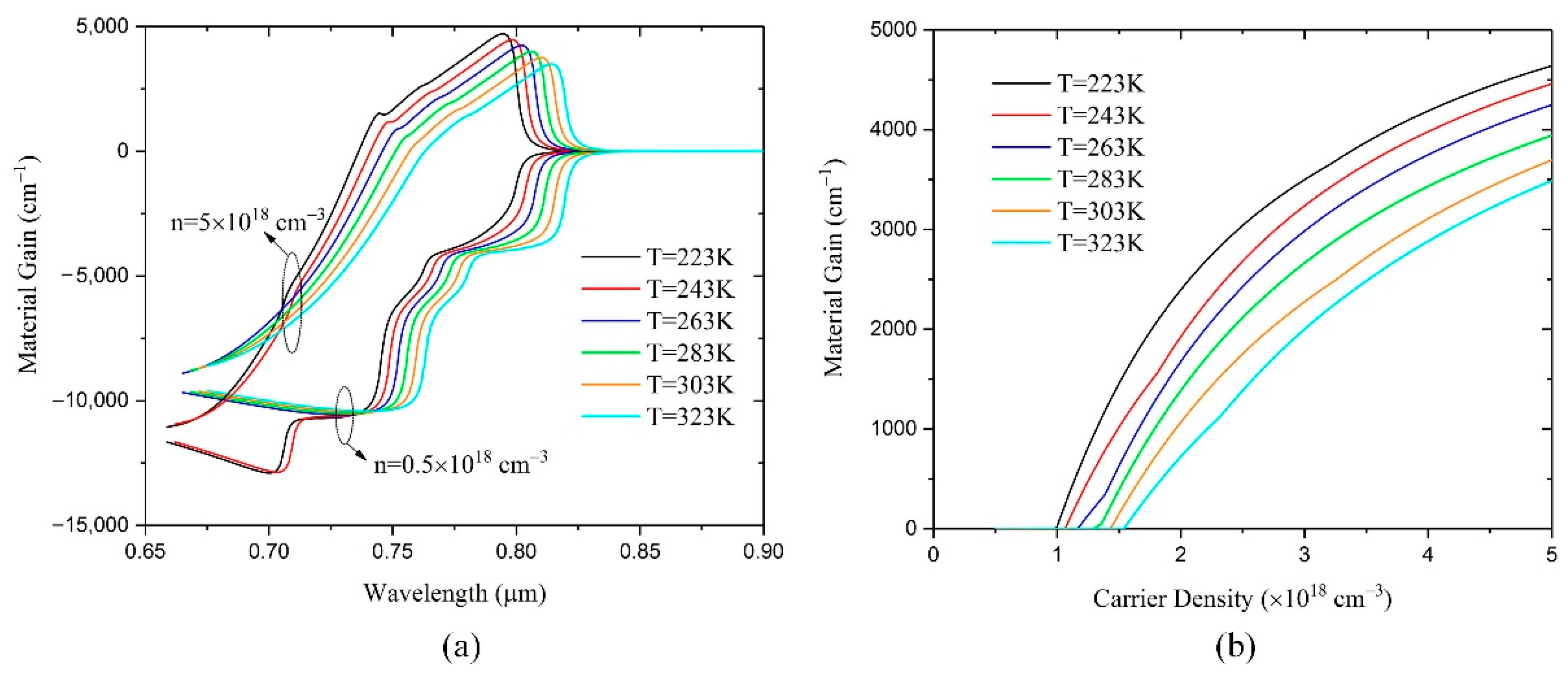
4.1. Temperature Effects in the Quantum Well

The temperature effects on the carrier leakage process and mode gain in the active region were first simulated and analyzed. Figure 1a shows the distribution of carrier concentration with energy level, which was calculated according to the model in Section 2, where the quantum barrier was Al0.25Ga0.75As and the temperature of the active region was 223 K. The position of the curve jump was the location of the quantum well sub-energy level, and the near-exponential decay was a distinctive feature of the Fermi-Dirac distribution. A high carrier confinement efficiency of 98% was obtained by calculating the proportion of the curve integral in the red bar area (i.e., the part below the quantum barrier height) to the total range. Figure 1b shows the variation in carrier confinement efficiency with the Al content of the quantum barrier at different temperatures, where the carrier confinement efficiency decreased exponentially as the Al content decreased from 0.35 to 0.1. The 96% carrier confinement efficiency was considered as an acceptable value in this design, as shown in Table 3. Thus, the operating temperature was a significant factor in the selection of the quantum barrier material. Since the Al content of 0.25 in the quantum barrier ensured 98% carrier confinement efficiency at 223 K, the followed simulations were based on the In0.14Al0.14Ga0.72As/Al0.25Ga0.75As quantum well.
The gain spectrum curves are shown in Figure 2. When the carrier concentration in the quantum well was 0.5 × 1018 cm−3, meaning the injection current was lower than the threshold current, the material gain was negative. When the carrier concentration increased to 5 × 1018 cm−3, the material gain at the lasing wavelength was positive and lasing occurred. In addition, as the temperature rose, the peak material gain gradually decreased, and red shifts of the lasing wavelength were observed. Figure 2b is drawn with the peak gain as the Y-axis to better illustrate the relationship between material gain, temperature, and carrier concentration. As the temperature rose from 223 to 323 K, the slope of material gain gradually decreased, and the transparent carrier density gradually increased from 0.98 × 10¹⁸ to 1.54 × 1018 cm−3, indicating the weaker gain capability of the quantum well.

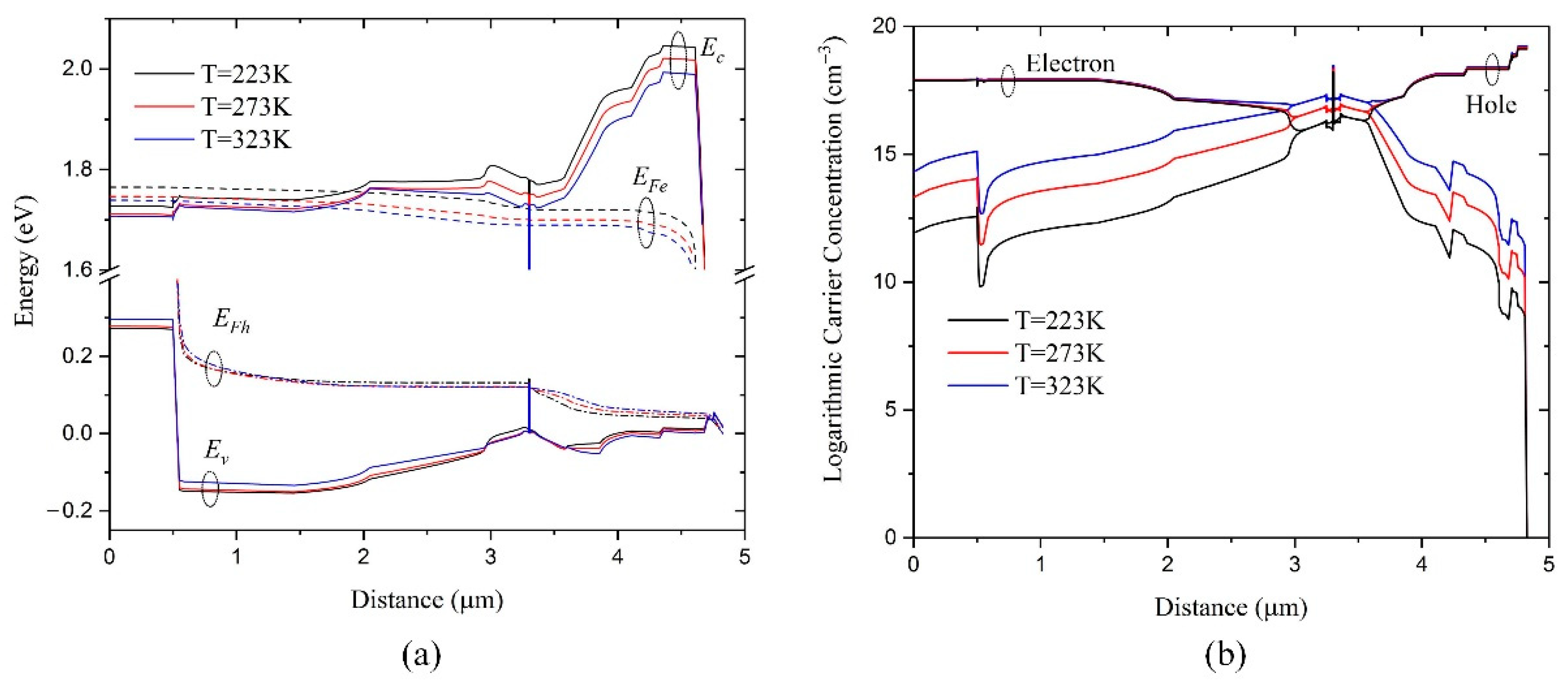
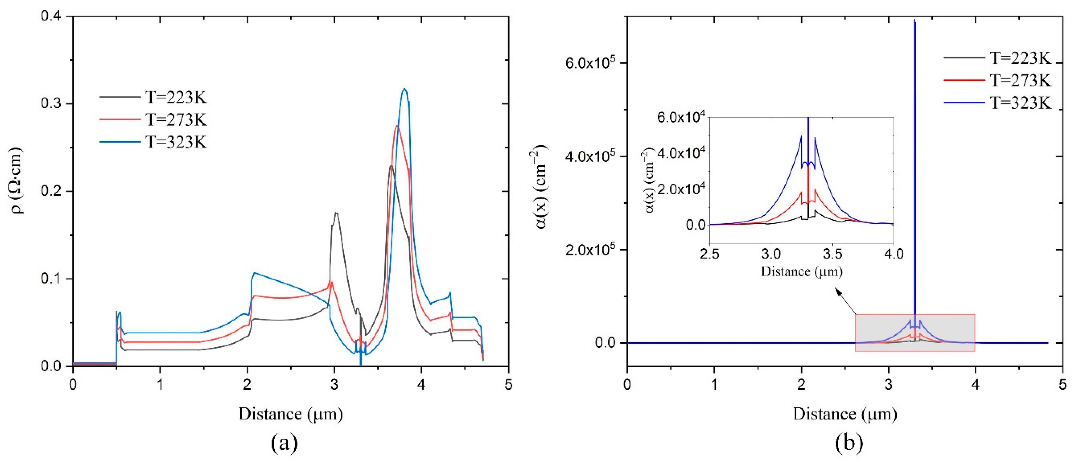
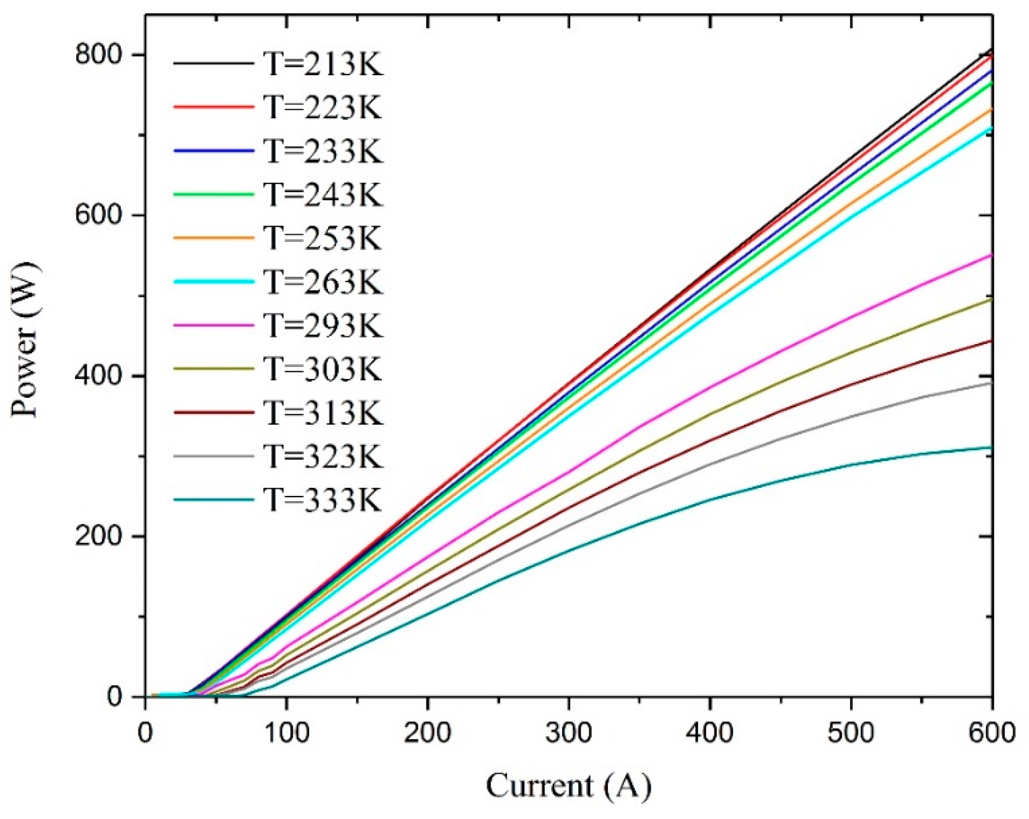
4.2. Temperature Effects in the Whole Epitaxial Direction

The carrier leakage in the quantum well was enhanced and the material gain decreased as temperature rose, which brought about a series of catastrophic chain reactions. Therefore, the trends in energy band structure, carrier concentration, electric resistivity, and free carrier absorption intensity with temperature were analyzed along the epitaxial direction, as shown in Figure 3 and Figure 4. According to the threshold gain condition of semiconductor lasers [15]:
Γ g t h ( T , n ) = α i + α m
The model gain must compensate for the optical loss in the resonant cavity, thus the carrier concentration injected into the quantum well must increase to compensate for the decrease in gain capability of the active region, which was consistent with the increase in carrier concentration and electron Fermi energy level illustrated in Figure 3.
The electric resistivity and free carrier absorption intensity are important indicators that affect the voltage and output power of the device. These two values will also be affected as the temperature changes the distribution of carrier concentration, as shown in Figure 4. The free carrier absorption intensity   α ( x ) is defined as follows [23],
α ( x ) = I ( x ) S [ σ n n ( x ) + σ p p ( x ) ] S = + I ( x ) d x
where I ( x ) , n ( x ) , and p ( x ) are the wave intensity, electron concentration, and hole concentration along the epitaxial direction, respectively. σ n and σ p are the absorption coefficients of free electrons and holes, respectively.
On the one hand, as the temperature increased, the resistivity of the local area near quantum well decreased, while the value of both N-cladding and P-cladding increased significantly, resulting in a rise of bulk resistance from 25.5 mΩ at 223 K to 36.9 mΩ at 323 K. On the other hand, the closer to the quantum well, the higher the free carrier absorption intensity and the higher contribution to the internal optical loss. The value of free carrier absorption intensity in the quantum well was approximately 50 times that of the waveguide at 223 K, mainly resulting from the high carrier concentration and wave intensity in the quantum well.

4.3. Temperature Effects on the Slop Efficiency

According to Equations (1) and (2), the carrier confinement efficiency needs to be combined with the radiation recombination efficiency and internal loss to determine the slop efficiency. Therefore, in order to compare the simulated and experimental data, the temperature effects on the radiation recombination efficiency and the internal loss were simulated in this section.
Figure 5 illustrates the position of the electron and hole Fermi energy levels in the quantum well at various temperatures. The electron Fermi energy level was approximately linear with temperature when the injection current was fixed at 10 A, and the fitted result was Ec − EFe = −0.0192 − 1.828 × 10⁻⁴T (eV). The hole Fermi energy level was approximately parabolic with temperature, and the fitted result was Ev − EFh = 0.02362 − 1.03878 × 10⁻⁴T + 1.78482 × 10⁻⁷T2 (eV).
The carrier concentration in the quantum well was clamped over the threshold; however, this clamped state was shifted by the temperature, as shown in Figure 6, which implied a nonlinear relationship between the threshold carrier concentration and temperature. The threshold carrier concentration increased exponentially from 1.60 × 10¹⁸ to 2.75 × 1018 cm−3 when the temperature rose from 223 to 323 K.
Figure 7 shows the trend in radiation recombination efficiency with injection current and temperature. The radiation recombination efficiency is derived from the formula:
η r a d   = R s p o n + R s t i m R s p o n + R s t i m + R a u g e r + R S H R
where R s p o n , R s t i m , R a u g e r , and R S H R represent the spontaneous radiation recombination rate, stimulated radiation recombination rate, Auger non-radiation recombination rate, and SHR non-radiation recombination rate, respectively. Each of them is affected by the carrier concentration in the quantum well. Therefore, under the threshold, the radiation recombination efficiency increased rapidly with the injection current before becoming stable. Additionally, it was exponentially reduced from 94.9% at 223 K to 92.6% at 323 K at an injection current of 10 A. This finding meant that as the temperature rose, the proportion of non-radiative recombination increased, and this part of the lost energy would eventually become the local thermal source in the chip to further reduce the carrier confinement efficiency and material gain.
Figure 8 shows the trend in internal optical loss accompanied by current and temperature. The internal loss is derived from the formula [24]:
α i = + α ( x ) d x + α s c a t
where α s c a t represents the scattering loss and α ( x ) is the free carrier absorption intensity defined in Equation (10). It can be estimated that the internal optical loss did not change significantly with the injection current after reaching the threshold current. The internal optical loss increased exponentially from 0.57 to 1.67 cm−1 as the temperature rose from 223 to 323 K. According to Equation (9), the threshold material gain has to increase since the optical confinement factor of the quantum well hardly changed with temperature. In summary, the material gain ability gradually weakened as the temperature increased, so the carrier concentration in the quantum well needed to increase, resulting in a corresponding increase in internal optical loss. Finally, increasing the carrier concentration in the quantum well is needed to achieve the new threshold gain condition, forming a vicious circle and causing the carrier concentration in the quantum well to increase exponentially. This is an important reason for the rapid decline in the performance of semiconductor lasers at high temperatures.

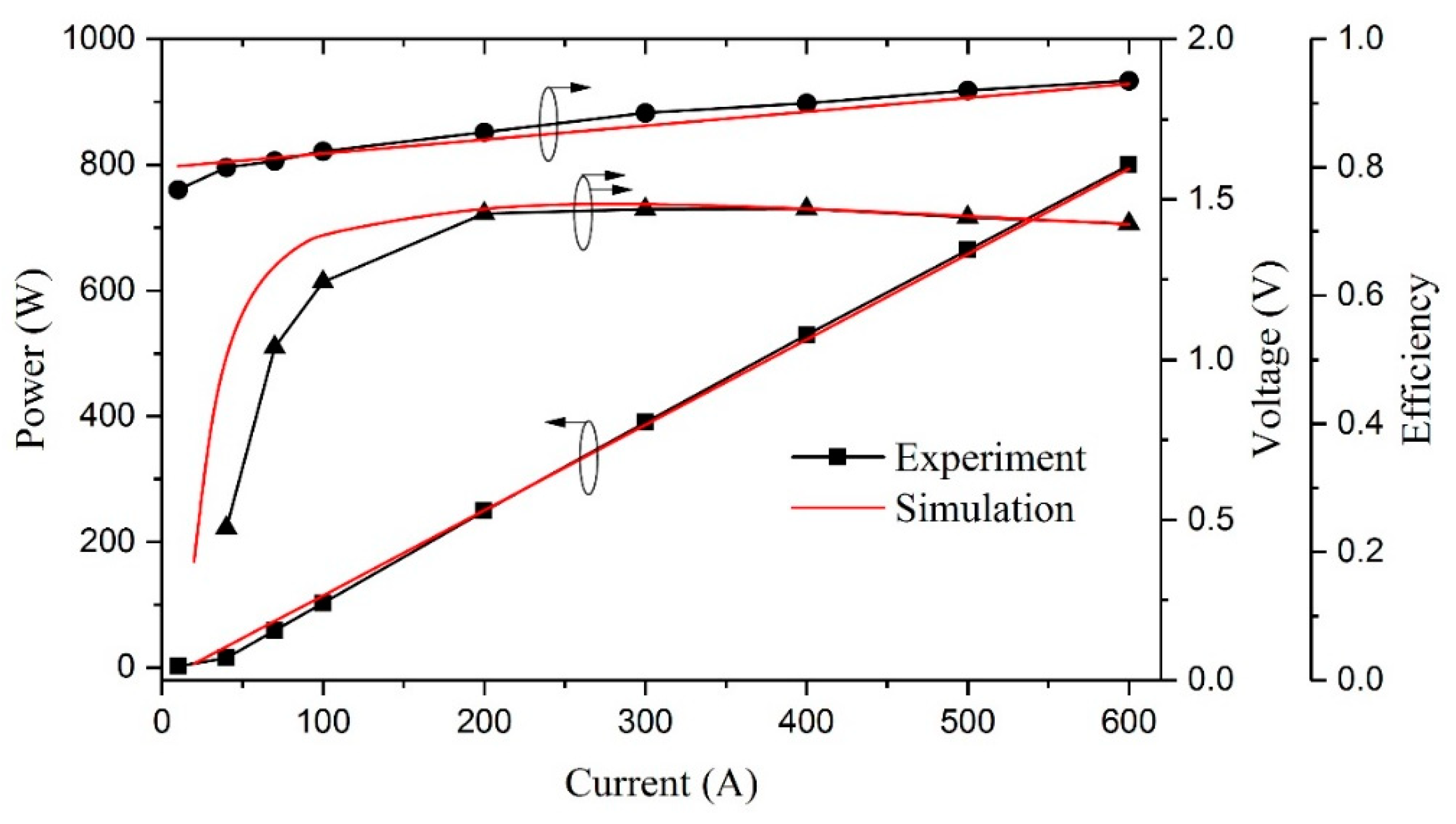
5. Contrast of Simulated and Experimental Data

In order to achieve a carrier confinement efficiency as high as 98% at 223 K, the Al content of the quantum barrier in Table 2 was optimized to be 0.25. The semiconductor laser with the optimized epitaxial structure was fabricated using a standard process. The laser bars with 44 emitting units and 2 mm cavity length were tested at heatsink temperatures ranging from 213 to 333 K in the quasi-continuous-wave (QCW) mode of 250 μs pulse and 200 Hz frequency.
Figure 9 shows the output power, injection current, and applied voltage (L-I-U) characteristics of the laser bar at 223 K compared with simulated values, which were deduced from the single-emitting simulation multiplier. According to the experimental results, the output power of the bar reached 799 W when the injection current was 600 A, while the electro-optical conversion efficiency was 71.2%. The device reached the maximum electro-optical conversion efficiency of 73.5% when the injection current was 400 A. The simulated and experimental results were highly consistent, indicating that the theoretical model we used in Section 2 and Section 4 accurately anticipated the performance of high-power semiconductor lasers.
The output power-current (L-I) curves ranging from 213 to 333 K are shown in Figure 10. The L-I curves showed an obvious linear relationship below a heatsink temperature of 273 K, with the slope efficiency rising from 1.25 W/A at 263 K to 1.34 W/A at 223 K. Additionally, the temperature effects of rising power were saturated below 213 K when the carrier leakage was almost negligible. The threshold current was increasing rapidly above a heatsink temperature of 293 K, from 41.7 A at 293 K to 70.5 A at 333 K, and the slope efficiency decreased significantly, from 1.09 W/A at 293 K to 0.81 W/A at 333 K. The output power dropped from 808 W at 213 K to 311 W at 333 K when the injection current was 600 A, with a difference of 497 W, meaning the device was only suitable for low temperatures.
The temperature of the active region was deduced using the method proposed in reference [25], and the detailed data is illustrated in Table 4. When the injection current was 600 A, the temperature of the active region was on average 30 K higher than the heatsink temperature. The trend in the threshold current and slope efficiency with the corrected temperature of the active region are illustrated in Figure 11. Both the variation in the threshold current and slope efficiency with temperature showed exponential forms, which were closely related to the exponential decay of the carrier confinement efficiency and material gain analyzed in Section 4.1. The simulated and experimental values were highly consistent in terms of temperature trends, indicating the reasonableness of the temperature effect analysis in Section 4. In addition, the simulation results in Section 4 were obtained by embedding the mathematical model in Section 2 into the simulation tools in Section 3, which further confirmed the accuracy of the newly proposed carrier confinement efficiency calculation model.
As for the absolute difference between the simulated and experimental values of the threshold current, this value mainly comes from the calculation deviation of the non-radiative recombination because the default non-radiative recombination parameters in the software material library were applied to calculate the radiation recombination efficiency. The non-radiative recombination rate is not only material dependent but also closely related to the quality of the epitaxial growth process, so it is usually roughly estimated. The fitting for the threshold current will be advanced in our future work to help better predict the device output characteristics.

6. Conclusions

The relationships among internal quantum efficiency, η i , model gain, Γ g 0 , and temperature T were analyzed theoretically and experimentally from the perspective of the active region of high-power semiconductor lasers. Based on the results obtained from different temperatures and injection currents, the following design guidelines were derived: (i) the carrier confinement efficiency will drop sharply when the barrier height is lower than a certain critical value, meaning optimization is necessary for the active region at different operating temperatures; (ii) the material gain of the active region decreases quickly as temperature rises, resulting in exponential soaring of carrier concentration and internal optical loss. The optimized design of the quantum well ensured that the carrier confinement efficiency reached 98% at 223 K and the carrier concentration in the quantum well was as low as 1.6 × 1018 cm−3, which further achieved a high radiation recombination efficiency of 95% and low internal optical loss of 0.57 cm−1 together with the optimized doping profile, achieving a high slope efficiency of 1.34 W/A. The output power of laser bars reached 799 W at 600 A injection current, while the electro-optical conversion efficiency reached 71%. The maximum electro-optical conversion efficiency of 73.5% was reached at the injection current of 400 A.

Author Contributions

Conceptualization, S.W. and T.L.; software, methodology, writing—original draft preparation, S.W.; writing—review and editing, T.L. and Z.W.; visualization, L.C. and J.Z. (Jiachen Zhang); investigation, J.Z. (Junyue Zhang) and J.L.; data curation, Y.Z. and L.D. All authors have read and agreed to the published version of the manuscript.

Funding

This work was supported by the National Natural Science Foundation of China (Grant No.61504167), the Natural Science Foundation of Shannxi Province, China (Grant Nos. 2019ZY-CXPT-03-05, 2018JM6010, and 2015JQ6263), and the Talent Project of Science and Technology Department of Shannxi Province (No.2017KJXX-72).

Data Availability Statement

The Data is not applicable due to confidentiality.

Acknowledgments

This work was performed within the project financially supported by the State Key Laboratory of Transient Optics and Photonics, Xi’an Institute of Optics and Precision Mechanics, Chinese Academy of Sciences. Additionally, we thank Xia from the Crosslight Company for his constructive guidance on the technical discussion and Yu for the provision of the experimental equipment. The simulation work was mainly supported by the Crosslight Company.

Conflicts of Interest

The authors declare that they have no conflict of interest.

References

  1. Ma, X.Y.; Wang, J.; Liu, S.P. Present situation of investigations and applications in high power semiconductor lasers. Infrared Laser Eng. 2008, 37, 189–194. [Google Scholar]
  2. Zhang, Y.; Hao, S.; Zhang, J.; Guo, C.; Wang, W. Study on the Application of Laboratory Environmental Test Methods for Military Materiel-GJB 150A—2009. China Personal Protective Equipment 2017, 03, 28–31. [Google Scholar] [CrossRef]
  3. Sotoodeh, M.; Khalid, A.H.; Rezazadeh, A.A. Empirical low-field mobility model for III–V compounds applicable in device simulation codes. J. Appl. Phys. 2000, 87, 2890–2900. [Google Scholar] [CrossRef]
  4. Vurgaftman, I.; Meyer, J.Á.; Ram-Mohan, L.Á. Band parameters for III–V compound semiconductors and their alloys. J. Appl. Phys. 2001, 89, 5815–5875. [Google Scholar] [CrossRef] [Green Version]
  5. Ho, C.H.; Li, J.H.; Lin, Y.S. Optical characterization of a GaAs/In0.5(AlxGa1-x)0.5P/GaAs heterostructure cavity by piezoreflectance spectroscopy. Opt. Express 2007, 15, 13886–13893. [Google Scholar] [CrossRef] [PubMed]
  6. Tansu, N.; Mawst, L.J. Current injection efficiency of InGaAsN quantum-well lasers. J. Appl. Phys. 2005, 97, 054502. [Google Scholar] [CrossRef] [Green Version]
  7. Laikhtman, B.; Gourevitch, A.; Donetsky, D.; Westerfeld, D.; Belenky, G. Current spread and overheating of high power laser bars. J. Appl. Phys. 2004, 95, 3880–3889. [Google Scholar] [CrossRef] [Green Version]
  8. Arafin, S.; Bachmann, A.; Vizbaras, K.; Hangauer, A.; Gustavsson, J.; Bengtsson, J.; Larsson, A.; Amann, M.C. Comprehensive analysis of electrically-pumped GaSb-based VCSELs. Opt. Express 2011, 19, 17267–17282. [Google Scholar] [CrossRef] [PubMed] [Green Version]
  9. Ryu, H.Y.; Ha, K.H. Effect of active-layer structures on temperature characteristics of InGaN blue laser diodes. Opt. Express 2008, 16, 10849–10857. [Google Scholar] [CrossRef] [PubMed]
  10. Song, Y.F.; Wang, Z.F.; Li, T.; Yang, G.W. Efficiency analysis of 808 nm laser diode array under different operating temperatures. Acta Phys. Sin. 2017, 66, 104202. [Google Scholar] [CrossRef]
  11. Frevert, C.; Crump, P.; Bugge, F.; Knigge, S.; Erbert, G. The impact of low Al-content waveguides on power and efficiency of 9xx nm diode lasers between 200 and 300 K. Semicond. Sci. Technol. 2016, 31, 025003. [Google Scholar] [CrossRef]
  12. Hasler, K.H.; Frevert, C.; Crump, P.; Erbert, G.; Wenzel, H. Numerical study of high-power semiconductor lasers for operation at sub-zero temperatures. Semicond. Sci. Technol. 2017, 32, 045004. [Google Scholar] [CrossRef]
  13. Wang, M.P.; Zhang, P.; Nie, Z.Q.; Liu, H.; Sun, Y.B.; Wu, D.H.; Zhao, Y.L. Analysis of Cryogenic Characteristics of High Power Semiconductor Lasers. Acta Phtonica Sin. 2019, 48, 0914002. [Google Scholar] [CrossRef]
  14. Wang, Z.; Li, T.; Yang, G.; Song, Y. High power, high efficiency continuous-wave 808 nm laser diode arrays. Opt. Laser Technol. 2017, 97, 297–301. [Google Scholar] [CrossRef]
  15. Chuang, S.L. Fundamentals of Semiconductor Lasers. In Physics of Photonic Devices, 2nd ed.; Jia, D.F., Wang, Z.Y., Sang, M., Yang, T.X., Eds.; Publishing House of Electronics Industry: Beijing, China, 2013; Volume 10, pp. 268–315. [Google Scholar]
  16. Zou, Y.; Osinski, J.S.; Grodzinski, P.; Dapkus, P.D.; Rideout, W.C.; Sharfin, W.F.; Schlafer, J.; Crawford, F.D. Experimental study of Auger recombination, gain, and temperature sensitivity of 1.5 μm compressively strained semiconductor lasers. IEEE J. Quantum Elect. 1993, 29, 1565–1575. [Google Scholar] [CrossRef]
  17. Romero, B.; Arias, J.; Esquivias, I.; Cada, M. Simple model for calculating the ratio of the carrier capture and escape times in quantum-well lasers. Appl. Phys. Lett. 2000, 76, 1504–1506. [Google Scholar] [CrossRef]
  18. Zbroszczyk, M.; Bugajski, M. Design optimization of InGaAlAs/GaAs single and double quantum well lasers emitting at 808 nm. In Proceedings of the Conference on Physics and Simulation of Optoelectronic Devices XII, San Jose, CA, USA, 26 January 2004; pp. 446–453. [Google Scholar]
  19. Tijero, J.M.G.; Borruel, L.; Vilera, M.; Consoli, A.; Esquivias, I. Simulation and geometrical design of multi-section tapered semiconductor optical amplifiers at 1.57 μm. In Proceedings of the Semiconductor Lasers and Laser Dynamics VI, Brussels, Belgium, 2 May 2014; p. 91342A. [Google Scholar]
  20. Calciati, M.; Debernardi, P.; Goano, M.; Bertazzi, F. Towards a comprehensive 3D VCSEL model: Electrical simulations with PICS3D. In Proceedings of the Fotonica AEIT Italian Conference on Photonics Technologies, Turin, Italy, 6–8 May 2015. [Google Scholar]
  21. Xia, C.S.; Li, Z.S.; Crosslight, Y.S. Effect of last barrier on efficiency improvement of blue InGaN/GaN light-emitting diodes. In Proceedings of the 13th International Conference on Numerical Simulation of Optoelectronic Devices, Vancouver, BC, Canada, 19–22 August 2013. [Google Scholar]
  22. Wu, S.H.; Li, T.; Wang, D.; Yu, X.C.; Wang, Z.F.; Liu, G.J. Optimization of the Epitaxial Structure of Low-Loss 885nm High-Power Laser Diodes. In Proceedings of the Sixteenth National Conference on Laser Technology and Optoelectronics, Shanghai, China, 31 August 2021; p. 53. [Google Scholar]
  23. Bulashevich, K.A.; Mymrin, V.F.; Karpov, S.Y.; Demidov, D.M.; Ter-Martirosyan, A.L. Effect of free-carrier absorption on performance of 808 nm AlGaAs-based high-power laser diodes. Semicond. Sci. Technol. 2007, 22, 502–510. [Google Scholar] [CrossRef]
  24. Pikhtin, N.A.; Slipchenko, S.O.; Sokolova, Z.N.; Tarasov, I.S. Internal optical loss in semiconductor lasers. Semiconductors 2004, 38, 360–367. [Google Scholar] [CrossRef]
  25. Johnson, L.A.; Teh, A. Measuring High Power Laser Diode Junction Temperature and Package Thermal Impedance; Application Note #30; ILX Ligthwave Corporation: Bozeman, MT, USA, 2008. [Google Scholar]
Figure 1. Simulated carrier confinement efficiency model: (a) the carrier concentration distribution with energy level for In0.14Al0.14Ga0.72As/Al0.25Ga0.75As quantum well at 223 K (b) carrier confinement efficiency vs. Al content of the quantum barrier at different temperatures.
Crystals 13 00085 g001
Figure 2. Temperature effects on material gain: (a) gain spectrum curves at different temperatures and injected carrier concentrations, (b) peak gain vs. injected carrier concentration at different temperatures.
Crystals 13 00085 g002
Figure 3. Temperature effects in the epitaxial direction at an injection current of 10 A (a) energy band structure (b) carrier concentration (the position of 0 μm is located at the start position of the N-buffer layer, while the ordinate of Figure 3a has a break range from 0.4 to 1.6 and the ordinate of Figure 3b is logarithmically transformed by 10).
Crystals 13 00085 g003
Figure 4. Temperature effects in the epitaxial direction at an injection current of 10 A (a) electrical resistivity, (b) free carrier absorption intensity.
Crystals 13 00085 g004
Figure 5. Temperature effects on Fermi energy level at an injection current of 10 A (a) electron Fermi energy level, (b) hole Fermi energy level.
Crystals 13 00085 g005
Figure 6. Temperature effects on electron concentration at the center of quantum well (a) electron concentration vs. injection current at different temperatures (b) electron concentration vs. temperature at an injection current of 10 A.
Crystals 13 00085 g006
Figure 7. Temperature effects on radiation recombination efficiency (a) radiation recombination efficiency vs. injection current at different temperatures (b) radiation recombination efficiency vs. temperature at an injection current of 10 A.
Crystals 13 00085 g007
Figure 8. Temperature effects on internal optical loss (a) internal optical loss vs. injection current at different temperatures, (b) internal optical loss vs. temperature at an injection current of 10 A.
Crystals 13 00085 g008
Figure 9. Contrast of simulated and experimental L-I-U curves of laser bars at 223 K.
Crystals 13 00085 g009
Figure 10. The experimental L-I curves of laser bars from 213 to 333 K.
Crystals 13 00085 g010
Figure 11. Comparison of simulated and experimental data of: (a) the threshold current, (b) the slope efficiency.
Crystals 13 00085 g011
Table 1. Main physical effects included in the simulations.
Physical EffectsNotes
Temperature dependence of energy band structureAdopting k-p theory
Carriers capture and escape process in the quantum wellDefined by electron and hole capture times
Temperature dependence of electron and hole mobilityAffected by temperature, carrier concentration and applied electric field
Main non-radiative recombinationIncluding Auger recombination and Shockley-Hall-Read (SHR) recombination
Temperature dependence of refractive indexAffected by temperature, carrier concentration and wavelength
Free carrier absorptionProportional to carrier concentration and wave intensity
Temperature dependence of material gainAffected by temperature, carrier concentration and spectrum
Temperature dependence of carrier concentrationDefined by Fermi-Dirac distribution, applying Poisson and continuity equations
Local heat sourcesNot included, treated as constant temperature and no thermal gradients
Table 2. Optimized epitaxial structure [22].
DescriptionMaterialsThickness
( μ m )
DopantDoping Concentration
(cm−3)
P-clapGaAs0.2C 3 × 10¹⁹→1 × 10²⁰
P-claddingAl0.4Ga0.6As-Al0.5Ga0.5As0.5C2 × 1018→4.5 × 10¹⁸
P-waveguideAlxGa1-xAs-Al0.4Ga0.6As0.8C 5 × 10¹⁶→2 × 10¹⁸
Quantum BarrierAlxGa1-xAs0.05UndopedNone
Quantum WellIn0.14Al0.14Ga0.72As0.008UndopedNone
Quantum BarrierAlxGa1-xAs0.05UndopedNone
N-waveguideAl0.35Ga0.65As-
AlxGa1-xAs
1.2Si 2 × 10¹⁷→5 × 10¹⁶
N-claddingAl0.35Ga0.65As1.5Si 2 × 10¹⁸→2 × 10¹⁷
N-bufferGaAs0.5Si2 × 1018
N-substrateGaAs150Si2 × 1018
Table 3. Al content of quantum barrier that satisfies η c o n = 96 % .
T (K)223243263283303323
Al Content0.2160.2300.2460.260.2740.288
Table 4. The temperature of the active region at different operating conditions.
T (K)
Heatsink
λ (nm)
I = 600 A
Waste Heat Power
(W)
T (K)
Active Region
Rth
(K/W)
213797.5827.74240.10.97
223799.7727.40249.20.95
233802.3728.86259.90.93
243804.9029.69270.30.92
253807.2630.80280.10.87
263810.0932.26291.80.89
293818.1145.27324.90.70
303819.1649.12329.20.53
313823.0653.27345.30.60
323825.3056.99354.50.55
333827.9962.95365.60.52
Disclaimer/Publisher’s Note: The statements, opinions and data contained in all publications are solely those of the individual author(s) and contributor(s) and not of MDPI and/or the editor(s). MDPI and/or the editor(s) disclaim responsibility for any injury to people or property resulting from any ideas, methods, instructions or products referred to in the content.

