Abstract
In recent years, two-dimensional (2D) layered transition metal dichalcogenides (TMDs) have received significant attention due to their exceptional electrical and optical properties. Among these 2D materials, ReS2 distinguishes itself through its unique optical and conductance anisotropy. Despite concerted efforts to produce high-quality ReS2, the unique interlayer decoupling properties pose substantial challenges in growing large-area ReS2 thin films, with the preparation of single layers proving even more complex. In this work, large-scale continuous monolayer and bilayer ReS2 films were successfully grown on mica substrates using low-pressure chemical vapor deposition (LPCVD). Photodetectors were fabricated using the prepared high-quality ReS2 films, and the devices presented stable photoresponse and enhanced response sensitivity. The production of continuous ReS2 atomic layers heralds promising prospects for large-scale integrated circuits and advances the practical application of optoelectronics based on 2D layered materials.
1. Introduction
Two-dimensional (2D) layered transition metal dichalcogenides (TMDs) are emerging semiconductors for next-generation electronics and optoelectronics due to their excellent properties [1,2,3,4]. Different from graphene, most sulfide- and selenide-based TMDs exhibit bandgaps spanning the visible to near-infrared spectral range [5,6]. In particular, MoS2 and WS2, which are among the most extensively studied 2D materials, demonstrate direct bandgap semiconductor characteristics when reduced to monolayer thickness. Therefore, these materials have attracted significant interest for their light–matter interactions and shown enormous potential in the application of optoelectronic devices.
With the development of exploration for new 2D materials, ReS2 emerges as a standout candidate among numerous 2D materials which benefits from its distinct optical and electrical anisotropies [7,8]. The low crystal symmetry of ReS2 imparts a unique energy band structure, leading to strong anisotropy in effective mass, conductance, mobility, and thermal conductivity. The laser cavity prepared using the nonlinear saturable absorption characteristics of ReS2 achieves a modulation depth of 44% and a saturation level of 8.4 MW/cm2 [9,10,11,12]. ReS2 also demonstrates glorious polarization sensitivity, making it suitable for linear dichroic photodetectors [13,14,15]. Additionally, ReS2 has minimal dependence on thickness for its optical bandgap [16,17,18,19], making it the optimal choice for photodetector applications. A polycrystalline ReS2-based photodetector exhibits a responsivity of 4 × 10⁻³ A/W and an external quantum efficiency (EQE) of 0.99% [20]. Furthermore, ReS2 shows promising possibilities for facilitating the exploration of unusual physical phenomena and contributing to the design of innovative functional devices. Therefore, the synthesis of large-scale and high-quality ReS2 atomic layers is indispensable.
The emergence of chemical vapor deposition (CVD) as a synthesis technique signals promising avenues for large-scale manufacturing. However, CVD-synthesized ReS2 typically forms discrete micro-scale dendritic structures [21,22,23] instead of continuous films. The asymmetric and out-of-plane growth of ReS2 can be ascribed to its distorted 1T (1T’) structure and weaker interlayer interaction. Most instances of ReS2 growth through CVD occur under atmospheric pressure, thus limiting the control of the thickness of the synthesized samples and posing challenges to repeatable large-scale growth [24,25,26]. The growth of ReS2 thin films using low-pressure CVD is also reported; however, the samples are thicker bilayer or multilayer ones [27,28]. For example, Liu et al. successfully manufactured a large-area thin-layer ReS2 film under reduced pressure [20]. However, studies on the growth of high-quality and large-area ReS2 films with single-layer thickness under low pressure remain a challenge.
In this work, we achieved the growth of large-area monolayer and bilayer ReS2 thin films on mica utilizing LPCVD. The conditions facilitated the growth of both monolayer and bilayer ReS2 films within a wide temperature range. Furthermore, we constructed ReS2 photodetectors, and the devices showed excellent performance. This study proposes a novel method for producing large-scale ReS2 atomic layers, fostering broader practical application possibilities for ReS2 electronic and optoelectronic devices.
2. Materials and Methods
2.1. Growth of ReS2
The growth of monolayer ReS2 was conducted in a two-temperature-zone LPCVD system, utilizing a quartz tube nesting in another quartz tube. ReO3 (1~2 mg) and S (1.5~2 g) powder were employed as precursors in the internal tube for the growth of ReS2. S powder was located in a quartz boat in low-temperature zone I. Mica substrate (1 cm × 1 cm) was arranged in the internal tube on a quartz plate in high-temperature zone II. An open-ended quartz boat with ReO3 precursor was situated within the same temperature zone adjacent to the mica substrate. A layer of molecular sieve (Na2O·Al2O3·2SiO2·4.5H2O) powder with a pore size of 0.4 nm covered the surface of ReO3 powder to regulate the release rate of the ReO3 source. During the growth process, the pressure of the quartz tube was approximately 1 Torr with 100 sccm high-purity Ar as carrier gas. The temperature of zone I was raised to 200 °C, and the temperature for zone II was raised to 700 °C and 600 °C for the growth of monolayer and bilayer ReS2, respectively. The growth process was sustained for 8 min. Following the growth phase, the samples cooled naturally to room temperature inside the furnace.
2.2. Characterizations of Samples
The characterization of ReS2 samples was performed with optical microscope (BX-51M, Olympus, Tokyo, Japan), atomic force microscope (Multimode8, Bruker, Bilerika, MA, USA), and transmission electron microscope (TecnaiG2 F30 S-TWIN, FEI, Hillsboro, OR, USA). Carbon films supported on copper grids served as the medium for TEM characterization, to which the ReS2 layer was transferred. The Raman spectra and PL spectra were determined employing a laser Raman spectrometer (inVia96Q857, Renishaw, Gloucestershire, UK) with an excitation laser wavelength of 532 nm.
2.3. Fabrication and Measurement of Photodetectors
Devices were fabricated by transferring ReS2 onto SiO2/Si substrate with pre-deposited Cr/Au (30 nm/100 nm) electrodes. The volt-ampere characteristic curve and the photoresponse of ReS2 devices under various laser irradiation conditions were tested using a multi-functional precision electronic timer (GCI-73, Daheng, Beijing, China) and a digital source meter (2635B, Keithley, Cleveland, OH, USA).
3. Results and Discussion
3.1. Growth and Characterization of ReS2 Film
Large-area uniform monolayer and bilayer ReS2 films were grown using LPCVD in an argon gas atmosphere with S powder and ReO3 powder as sulfur and rhenium reaction sources, and the experimental setup is schematically illustrated in Figure 1a. Compared with atmospheric pressure CVD, LPCVD offers more precise control over the carrier gas, a cleaner reaction atmosphere, and reduced gas turbulence, which accelerates the transfer rate of gaseous reactants and enhances the reaction rate of thin film formation. Fluorophlogopite Mica (KMg3AlSi3O10F2) is employed as a substrate which has been proven to be a suitable candidate for crystal growth due to its inert and dangling-bond-free surface, as well as matched symmetry. Prior to growth, the freshly cracked mica was pre-treated via annealing in air to remove any remaining K+ ions on the surface and reduce the number of heterogeneous nucleation sites. This pre-treatment facilitates the lateral growth mode and promotes the epitaxial growth of large-area and high-quality ReS2 films [29]. It is worth noting that the positions of ReO3, sulfur precursors, and mica substrates were strategically arranged. The sulfur powder was located upstream in zone I and the ReO3 and mica substrates were placed downstream in zone II. The distance between sulfur and ReO3 is 25 cm, and the distance between ReO3 and the center of the substrates is 3 cm. During the process of growth, the mica substrates were placed horizontally on the sample holder. Compared with placing the substrate above the reaction source, positioning the substrate downstream horizontally helps to overcome the issue of uneven growth caused by the evaporation of the reaction source, as shown in Figure S1a. This substrate layout promotes the growth of large, uniform, and flat films, maximizing the utilization of mica substrates. It is notable that by employing this substrate placement method, ReS2 films can be synthesized over multiple mica substrates simultaneously, thereby greatly improving the synthesis efficiency of ReS2 films.
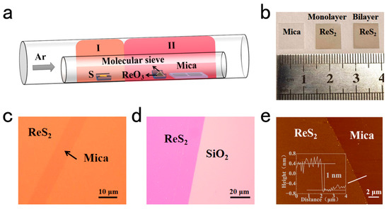
Figure 1.
(a) Schematic diagram of the experimental setup for the growth of ReS2 thin films via low-pressure CVD. I and II are low-temperature zone and high-temperature zone, respectively. (b) Photographs of bare mica substrate and monolayer and bilayer ReS2 films on mica. (c) Optical microscope (OM) image of monolayer ReS2 on mica substrate. (d) Optical microscope image of transferred ReS2 on SiO2 substrate. (e) AFM image of monolayer ReS2 on mica substrate.
In addition, we adopted a dual gas intake system for the growth of ReS2, and a photo of the dual gas intake is presented in Figure S1b. The quality of film is improved thanks to the designed gas intake system, which ensures more stable and uniform gas flow. When only a single gas intake is used, turbulence often occurs in the high-temperature region, leading to uneven growth, as shown in Figure S1c. Note that molecular sieves served to regulate the evaporation rate of ReO3, which effectively suppressed the nucleation density of ReS2. When the temperature exceeds 400 °C, ReO3 decomposes into evaporable Re2O7 and non-volatile ReO2 through the disproportionation reaction [25]. The equation of the reaction is:
Rapidly volatilizing Re2O7 is partially sulfurized and adsorbs on the substrate surface, furnishing numerous nucleation sites for the subsequent growth of ReS2. The amount of precursors was also skillfully adjusted to ensure uniform growth conditions. We finally fixed the growth parameter, including the amount and ratio of reaction sources, the distance between each reaction source and the substrate, and the flow rate of carrier gas, while changing the growth temperature of ReS2. Based on the contrast experiments, it was determined that the monolayer and bilayer film could be optimally produced at growth temperatures of approximately 700 °C and 600 °C, respectively.
3ReO3 → Re2O7 + ReO2
A photograph of monolayer and bilayer ReS2 films and bare mica substrate is presented in Figure 1b and the ReS2 atomic layers are clean and homogeneous. Figure 1c is an optical microscope image for the ReS2 monolayer grown on mica substrate with an artificial scratch made by tweezers, and the film shows a smooth and uniform surface. The color contrast between the ReS2 film and the exposed mica substrate is evident, which confirms the presence of a single-layer ReS2 film on the mica surface. Note that the thickness of the ReS2 film can only be roughly judged in advance using color comparison. The specific thickness of the film needs to be further tested with atomic force microscope (AFM) measurements. Optical microscope images of bilayer ReS2 films are shown in Figure S2a and the film also exhibits clean and uniform morphology. For more information on the growth of ReS2 on other substrates, please refer to Figure S2b,c. ReS2 films transferred to SiO2, whether through the water-assisted method [30] (Figure 1d) or employing the wet transfer method [31,32] (Figure S2d), exhibit an intact and uniform appearance under the optical microscope, confirming their excellent stability and mechanical strength.
An AFM image of the ReS2 film on mica is presented in Figure 1e, and the thickness of the ReS2 film is determined by measuring the height of the step at the scratched site, which is approximately 1 nm. It has been documented that the thickness of monolayer ReS2 exfoliated from bulk crystals is 0.7 nm, suggesting that the fabricated ReS2 thin film comprises one single layer [17]. The discrepancy in the thickness between the grown ReS2 and the exfoliated ReS2 results from the small gap between the grown ReS2 and the mica substrates. In addition to the gap on the interface, the roughness on the surface of the large-area continuous grown film also prompts the slight increase in the thickness. Please also see the AFM image of the bilayer ReS2 film shown in Figure S3. Both optical microscopy images and AFM characterizations substantiate the successful synthesis of large-area ReS2 films comprising highly uniform monolayers or bilayers.
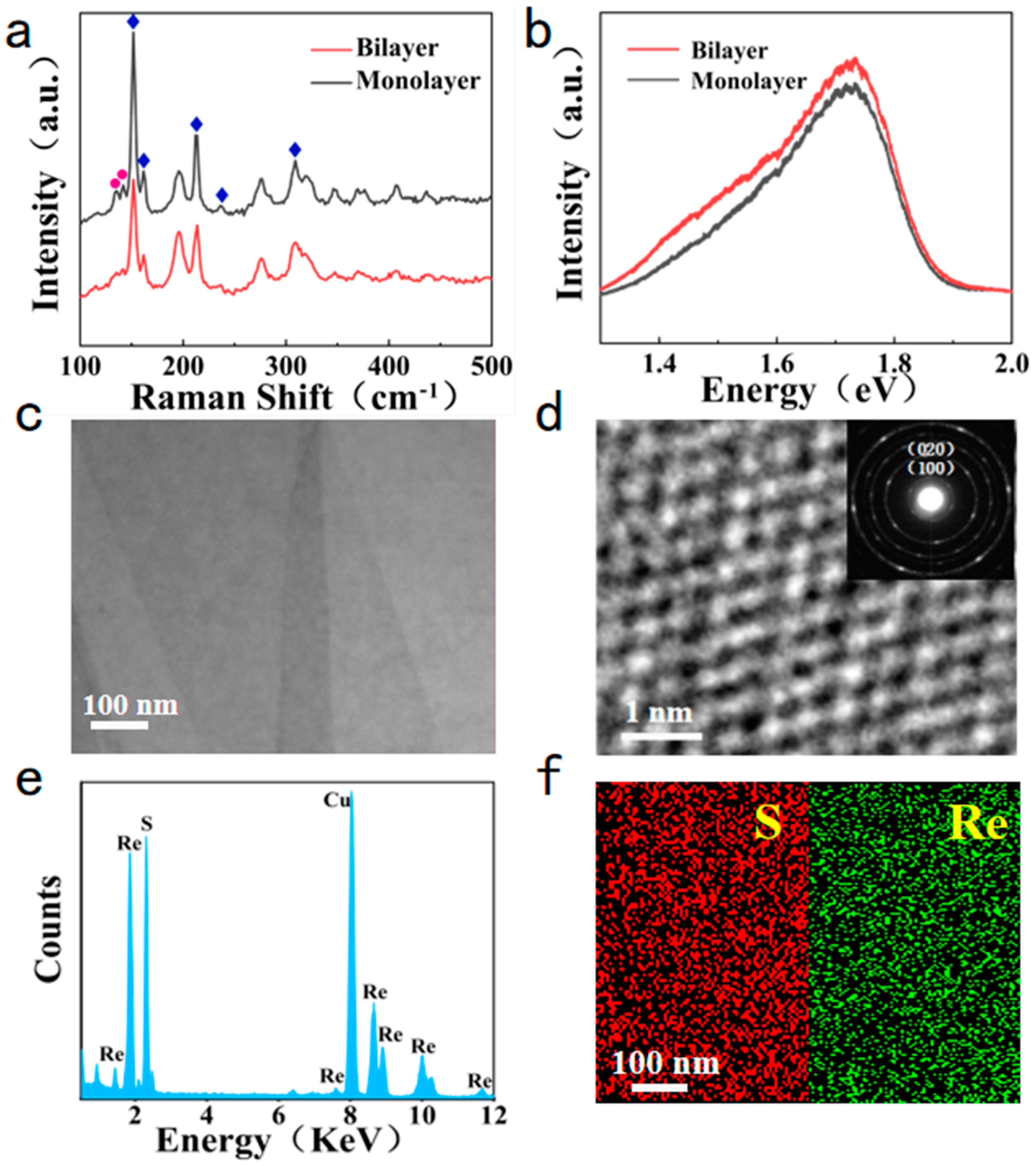
Raman spectroscopy has emerged as a vital tool for the rapid and lossless identification of layer numbers and for the evaluation of crystal quality for synthesized materials. The Raman signal of ReS2 was collected from the sample grown on mica substrate, revealing approximately 18 vibrational modes in the spectrum. Theoretically, these modes can be classified into in-plane (Eg), out-of-plane (Ag), and coupled in-plane and out-of-plane (Cp) vibrational modes. Vibrations below 250 cm−1 are attributable to the movement of Re atoms, while those above 250 cm−1 primarily result from the motion of S atoms [33]. In the case of monolayer ReS2, the phonon dispersion spectrum predicts the most pronounced intralayer Eg-like and Ag-like Raman modes [34]. Figure 2a is the Raman spectra for monolayer and bilayer ReS2. Five peaks, located at 151.7, 161.5, 213.6, 236.4, and 309 cm−1, correspond to the in-plane vibrations Eg, and two peaks at 135.3 and 141.8 cm−1 correspond to the out-of-plane vibrations Ag. In comparison with the previously reported Raman spectrum of ReS2 monolayers, the Raman peaks of the grown monolayer ReS2 in this work align closely with those typical Raman peaks, as presented in Table S1 [35,36]. In addition, the remaining high-frequency Raman peaks arise from the slight vibrations of S atoms and coupled in-plane and out-of-plane vibration modes of Re atoms [33]. Note that the peak located at 197.5 cm−1 is attributed to the signal from the mica substrate, as evidenced in Supplementary Figure S4 for the measurement of the Raman spectra of mica and the comparison of the Raman signal for pristine ReS2 on the mica substrate and transferred ReS2 on the silicon substrate. In summary, the synthesized ReS2 sample demonstrates well-defined Raman peaks, which indicates the excellent crystal quality of the samples.

Figure 2.
(a) Raman spectra of monolayer and bilayer ReS2 on mica substrate. (b) PL spectra of monolayer and bilayer ReS2 films on mica substrates. (c) TEM image of ReS2 thin film. (d) Magnified crystal structure of ReS2 transformed with FFT. The inset is the corresponding SAED pattern. (e) EDS spectrum of ReS2 film. (f) EDS mapping of S and Re.
Moreover, the ReS2 samples demonstrated intense photoluminescence (PL) emission at room temperature. Figure 2b is the PL spectra of monolayer and bilayer ReS2 films, and the positions of the PL peaks for both samples are approximately 1.73 eV. The photoluminescence intensity experiences a mild decrease for the ReS2 monolayer compared with that of the ReS2 bilayer, which attributes to the direct bandgap and interlayer decoupling features of ReS2. Contrary to traditional Mo- and W-based TMDs, the intensity of the PL peak in ReS2 films does not decline with the increased layer number [17].
Transmission electron microscopy (TEM) was employed for further analysis of the crystal structure of ReS2 films. Due to the weak adhesive force between the ReS2 film and mica substrate, the water-assisted transfer method was adopted to move the ReS2 monolayer onto a carbon-film-coated copper grid. Figure 2c is a TEM image of the ReS2 film, showcasing a neat, consistent, and expansive continuous monolayer film. The presence of the creases in the film akin to the edge folding phenomenon observed in TEM analyses of other two-dimensional materials, such as MoS2 and graphene [37], implies that the creases may be an artifact of the transfer process. Figure 2d presents an enlarged image obtained with fast Fourier transform (FFT) of the TEM selection area. The image reveals that the crystal structure of ReS2 follows a parallelogram-shaped 1T’ structure in accordance with the Re4 cluster growth mode [38]. Two distinct diffraction rings were displayed in the selected area electron diffraction (SAED) pattern, corresponding to the (100) and (020) crystal planes in the 1T’ structure, providing evidence of numerous randomly oriented grains within the film [20]. Please also refer to Figure S5 for more TEM images of ReS2 films. This observation further confirms that the coalescence of these arbitrarily oriented ReS2 grains leads to the formation of uniform polycrystalline films. For the purpose of discerning the grain size, high-resolution transmission electron microscopy (HRTEM) measurements of the ReS2 film were performed. Figure S6 presents the HRTEM image, and the average grain size of ReS2 is about 3.8 nm. Furthermore, the orientations of grains are random without preferred directions.
The constituent elements of the synthesized samples were analyzed using an energy dispersive spectrometer (EDS) to determine their type and content. As shown in Figure 2e, the signals of Re and S were easily detected. Note that the signal of the Cu element comes from the copper grid. The atomic percentage of Re and S were 32.41% and 67.59%, respectively, with a ratio of approximately 1:2. The results of EDS confirm that the sample is ReS2. Please also see Table S2 for more information. EDS element mapping is presented in Figure 2f, which demonstrates the high quality of the low-pressure CVD-grown ReS2 with Re and S elements evenly distributed throughout the entire sample.
3.2. Optoelectronic Properties of ReS2 Films
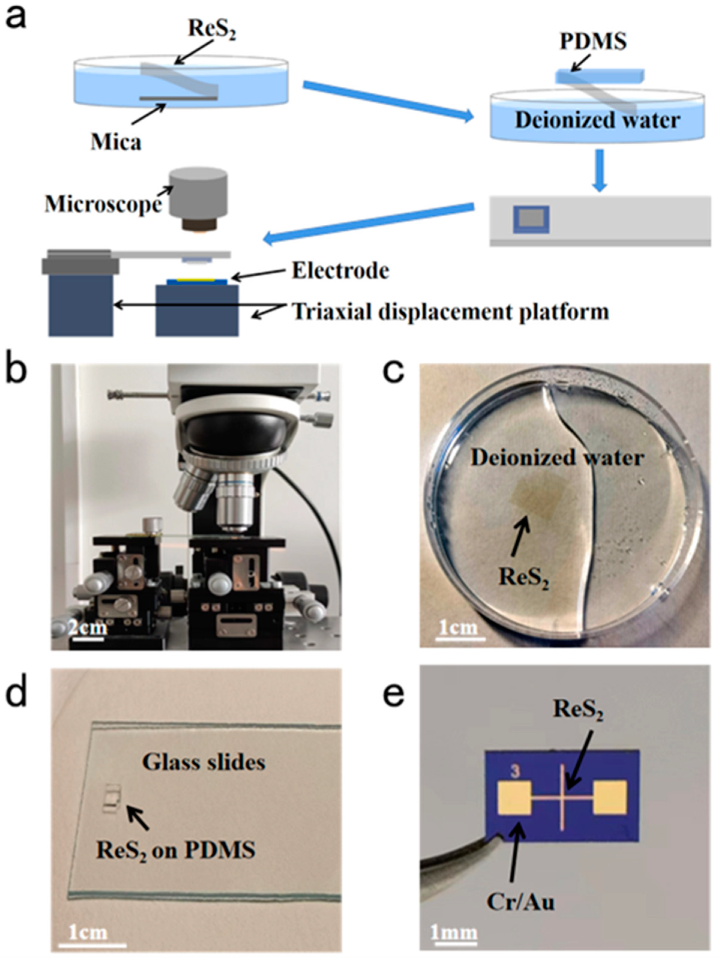
In order to figure out the optoelectronic properties of the as-grown ReS2 atomic layers, we fabricated ReS2 photodetectors by implementing a water-assisted transfer technique. The fabrication process is depicted in Figure 3a, and Figure 3b is the photograph of the triaxial displacement system. The ReS2 film grown on a mica substrate can be easily detached from the substrate utilizing the water-assisted method owing to the weak binding force between ReS2 and mica. Notably, Figure 3c illustrates the peeled ReS2 film in deionized (DI) water, which remarkably retains its integrity and cleanliness. Subsequently, Polydimethylsiloxane (PDMS) film was employed to conglutinate the ReS2 film from the surface of DI water. When attaching the ReS2 film with PDMS, it is crucial to handle the ReS2 film with care, which helps to prevent the film from curling or folding during the transfer process. The PDMS film containing the ReS2 film was then affixed to a glass slide, which is shown in Figure 3d. Due to the strong bonding force between the ReS2 and silicon substrate, it is effortless to transfer the ReS2 film from PDMS onto silicon substrate. Note that the strong binding force between ReS2 and SiO2 substrate here is a relative concept. Compared with the binding force between ReS2 and PDMS, the binding force between ReS2 and SiO2 is stronger. Therefore, the ReS2 film attached on the PDMS is easily transferred onto SiO2. The origin of the interaction between ReS2 and the substrate comes from the van der Waals force, which is the attraction caused by the uneven distribution of charges between molecules. The difference in bonding forces may attribute to the diversity in the distribution of charges between different molecules. The fabrication of ReS2 photodetectors was realized through the directional transfer of ReS2 onto the target location on silicon wafers with prefabricated electrodes using the triaxial displacement system, and Figure 3e presents a photograph of the ReS2 photodetector with Cr/Au electrodes on a silicon substrate. Notably, this technique effectively minimizes potential contaminations from the fabrication process of devices, such as photoresist for photolithography and polymethyl methacrylate (PMMA) for wet transfer. Furthermore, this method simplifies the fabrication process and reduces the manufacturing cost of optoelectronic devices. The water-assisted transfer technique allows for the reuse of the mica substrate after exfoliation. Large-area, uniform, and continuous ReS2 films can still be grown on the used mica substrates, which significantly saves the consumption of substrates. Figure S7 presents an AFM image of the ReS2 film grown on a reusable mica substrate. In addition, the water-assisted transfer method also offers convenience for TEM characterization. It is important to note that the thin layer of ReS2 may be susceptible to damage during the wet transfer process, particularly causing issues with the adhesion of films onto the copper grid. To overcome this challenge, the water-assisted transfer method enables the direct capture of large-area ReS2 films using copper grids. This approach reduces the difficulty of preparing TEM samples and facilitates the characterization of the morphology and lattice structure of samples.
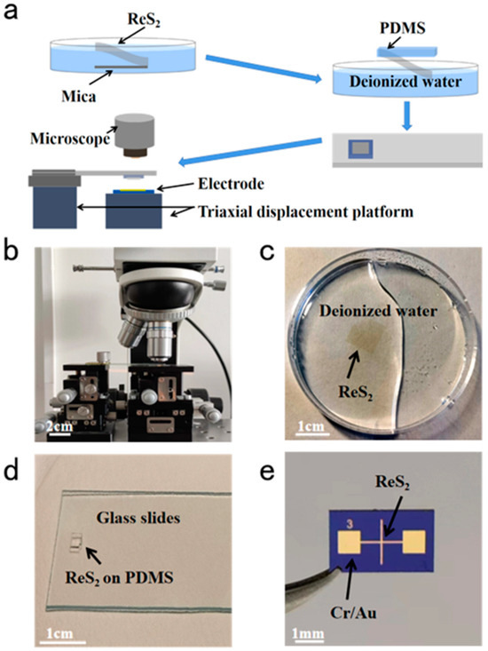
Figure 3.
(a) Flow chart of water-assisted transfer for ReS2 film. (b) Photograph of the self-made triaxial displacement system. (c) ReS2 film exfoliated from mica substrate via water-assisted transfer method. (d) Glass slide with ReS2/PMDS films on the surface. (e) ReS2 photodetector with Cr/Au electrodes on silicon substrate.
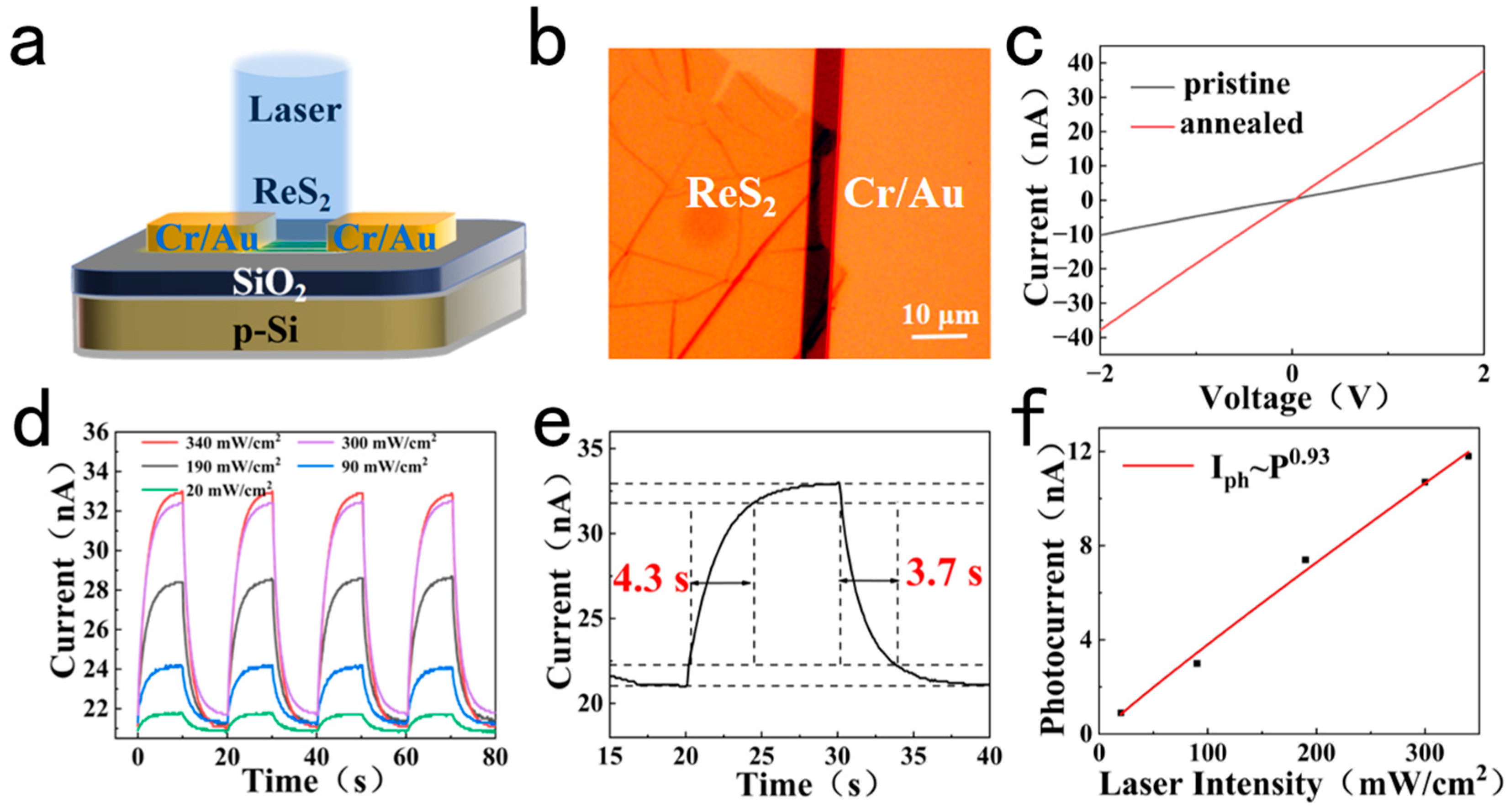
Compared with ReS2 monolayers, few-layer and bulk-like ReS2 has been exploited in high photoresponsivity detectors operating within the visible range owing to their higher light absorption along with the existence of trap states [39,40,41]. Therefore, the as-grown bilayer ReS2 films were used to fabricate photodetectors. ReS2 photodetectors were prepared directly on a SiO2/Si substrate with prefabricated Cr/Au (30/100 nm) electrodes using the water-assisted transfer technique. The SiO2/Si substrate consists of P-type heavily doped silicon with a 300 nm SiO2 oxide layer on its surface. Figure 4a depicts a schematic diagram of the device, while Figure 4b presents an optical microscope image of the device. The channel length of the device is 5 μm. The I-V characteristic curve of the ReS2 photodetector in Figure 4c exhibits a linear shape and voltage symmetry, suggesting the formation of reliable ohmic contact between ReS2 and the electrodes. Subsequently, we annealed the devices in the Ar atmosphere, resulting in a significant improvement in the magnitude of the current. The noted improvement is attributable to the annealing effect. Annealing of the prepared ReS2 thin film results in an increase in the grain sizes of ReS2. This phenomenon occurs as smaller grains show the tendency to combine and form larger grains at high temperatures. The grain size plays a significant role in the conductivity because the energy barrier forms at the grain boundary. The amount of grain boundary decreases with the enlargement of grain sizes; thus, the energy barriers decrease. Consequently, the reduction in energy barriers enhances the mobility of electrons, thus improving the conductivity of ReS2 [42]. Additionally, we encapsulated the ReS2 photodetectors using PMMA. Compared with exposed devices, the encapsulated ReS2 devices exhibit equally outstanding electrical performances and photoelectric responses. Figure S8 shows the optical microscope image and I-V curves of the device after packaging. Similarly, an annealing treatment was also performed on the encapsulated ReS2 photodetector, resulting in an improvement in the current as well. Encapsulation technology not only prevents environmental pollution to the material but also inhibits the oxidation of the sample.
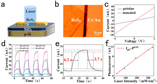
Figure 4.
(a,b) Schematic diagram and optical microscope image of the photodetector. (c) I-V characteristic curves of the device before and after annealing at 200 °C for 2 h in Ar atmosphere. (d) Switching characteristic curves for ReS2 photodetector under 450 nm incident light with different optical power densities. (e) Measurement of rise time and decay time with 10% margin. (f) The relationship between device photocurrent and incident light power density.
Previous studies on the optoelectronic properties of ReS2 mainly focused on single-crystal ReS2, while relatively little attention was paid to the properties of polycrystalline ReS2 [23,43,44]. In this work, high-power laser photodetections were conducted for polycrystalline bilayer ReS2 films utilizing a laser with a wavelength of 450 nm, which is illustrated in Figure 4d. The switching time of the laser was set to be 10 s with optical power densities of 340, 300, 190, 90, and 20 mW/cm2, and the bias voltage was maintained at 2 V. The ReS2 photodetector exhibited a consistent, stable, and repeatable response to the laser light. Despite the potential for high-power lasers to damage optoelectronic devices composed of two-dimensional materials, the ReS2 photodetectors prepared in this work demonstrated commendable stability under high-power lasers.
For photodetectors, responsivity (Rλ) is defined as Rλ = Iph/PS, where Iph represents the generated photocurrent (Iph = Ilight − Idark) and P is the optical power density impinging on the active region (S) of the device. The external quantum efficiency is calculated with the equation EQE = hcRλ/eλ, where the parameters h, c, λ, and e are the Plank constant, speed of light, wavelength of incident light, and charge of electron, respectively. In our study, Iph, P, and S were determined to be 11.7 nA, 340 mW/cm2, and 100 μm2, respectively. Consequently, under the incidence of the laser with a wavelength of 450 nm, the maximum Rλ for the ReS2 photodetector was determined to be 3.4 × 10⁻² A/W and the value of EQE is 9.38%. As discernible from Figure 4e, the device displays a relaxation time in response to the high-power laser. The rise/decay times of the photodetector, defined as the time for the current to increase/decrease from 10% to 90% of the steady value, are 4.3 s and 3.7 s, respectively, which is presented in Figure 4e. This phenomenon can be attributed to the properties of polycrystalline films, which are characterized by a multitude of grain boundaries. Defects around these grain boundaries form trap states, decelerating the migration of photogenerated carriers and thereby diminishing the response speed. The relationship between the photocurrent Iph and the incident laser power density P can be described with the formula Iph = Pα, where α represents fitting parameters. Figure 4f shows the relationship between the device photocurrent and incident laser power density when an external voltage of 2 V is applied. Notably, the optimal fitting result yields α as 0.93. The exponent α typically falls within the range of 0 to 1, reflecting complex processes that encompass the generation, separation, and recombination of photogenerated electron–hole pairs [45].
4. Conclusions
In conclusion, this work achieves successful growth of large-scale ReS2 atomic layers on mica substrates using low-pressure chemical vapor deposition. Morphology characterizations have confirmed the excellent cleanliness, integrality, and homogeneity of the continuous films. Moreover, ReS2 photodetectors were fabricated employing the water-assisted transfer technique. Demonstrating a distinct photoresponse under a laser bias voltage of 2.0 V at a wavelength of 450 nm, the ReS2 photodetector exhibits a rise time of 4.3 s, a decay time of 3.7 s, a photoresponse rate of 3.4 × 10⁻² A/W and an external quantum efficiency of 9.38%. Remarkably, it retains its stability even under the exposure of high-power lasers, showcasing the consistent optoelectronic performance, which makes ReS2 a promising candidate for practical application in high-performance photodetectors.
Supplementary Materials
The following supporting information can be downloaded at: https://www.mdpi.com/article/10.3390/cryst13111548/s1, Figure S1: Comparison of substrate position and gas intake system, Figure S2: Optical microscope images of ReS2 on various substrates, Figure S3: AFM image of large-area bilayer ReS2 film, Figure S4: Raman spectra of ReS2 and mica, Figure S5: TEM images of ReS2 film, Figure S6: High-resolution TEM image of ReS2 with the grains marked by the dotted boxes, Figure S7: AFM image of a ReS2 thin film grown repeatedly on reusable mica, Figure S8: Comparison of I-V characteristic curves of encapsulated device, Table S1: Raman peak positions in ReS2 [35,36], Table S2: Ratio of Re and S elements in the film.
Author Contributions
Conceptualization, Z.W., Y.L. and Z.Z.; Formal analysis, X.S., E.A., Z.W., Y.W. (Yingying Wang) and Y.L.; Funding acquisition, Z.W., S.W., Y.W. (Yingying Wang) and Z.Z.; Methodology, X.S., E.A., Z.W. and Y.L.; Resources, Y.W. (Yang Wen), S.W., Y.C., Y.W. (Yingying Wang), Y.L. and Z.Z.; Supervision, Z.W.; Validation, X.S.; Writing—original draft, X.S.; Writing—review and editing, Z.W. and Y.L. All authors have read and agreed to the published version of the manuscript.
Funding
This research was funded by the National Natural Science Foundation of China, grant numbers 52171229 and 12204084; the Liaoning Province Applied Basic Research Program, grant number 2023JH2/101600045; the Liaoning Province Education Department Basic Scientific Research Project, grant number LJKQZ20222301; the Liaoning Education Department Scientific Research Fund Project, grant number JDL2020012; the Dalian Science and Technology Innovation Fund, grant number 2022RQ025; and the Shandong Provincial Natural Science Foundation, grant number ZR2020MF122.
Data Availability Statement
The data presented in this study are available on request from the corresponding author.
Conflicts of Interest
The authors declare no conflict of interest.
References
- Chhowalla, M.; Shin, H.S.; Eda, G.; Li, L.-J.; Loh, K.P.; Zhang, H. The chemistry of two-dimensional layered transition metal dichalcogenide nanosheets. Nat. Chem. 2013, 5, 263–275. [Google Scholar] [CrossRef] [PubMed]
- Jariwala, D.; Sangwan, V.K.; Lauhon, L.J.; Marks, T.J.; Hersam, M.C. Emerging device applications for semiconducting two-dimensional transition metal dichalcogenides. ACS Nano 2014, 8, 1102–1120. [Google Scholar] [CrossRef] [PubMed]
- Han, G.H.; Duong, D.L.; Keum, D.H.; Yun, S.J.; Lee, Y.H. van der Waals metallic transition metal dichalcogenides. Chem. Rev. 2018, 118, 6297–6336. [Google Scholar] [CrossRef] [PubMed]
- Jariwala, D.; Davoyan, A.R.; Wong, J.; Atwater, H.A. Van der Waals materials for atomically-thin photovoltaics: Promise and outlook. ACS Photonics 2017, 4, 2962–2970. [Google Scholar] [CrossRef]
- Chaves, A.; Azadani, J.G.; Alsalman, H.; Da Costa, D.; Frisenda, R.; Chaves, A.; Song, S.H.; Kim, Y.D.; He, D.; Zhou, J. Bandgap engineering of two-dimensional semiconductor materials. Npj 2D Mater. Appl. 2020, 4, 29. [Google Scholar] [CrossRef]
- Wang, Q.H.; Kalantar-Zadeh, K.; Kis, A.; Coleman, J.N.; Strano, M.S. Electronics and optoelectronics of two-dimensional transition metal dichalcogenides. Nat. Nanotechnol. 2012, 7, 699–712. [Google Scholar] [CrossRef]
- Rahman, M.; Davey, K.; Qiao, S.Z. Advent of 2D rhenium disulfide (ReS2): Fundamentals to applications. Adv. Funct. Mater. 2017, 27, 1606129. [Google Scholar] [CrossRef]
- Li, X.; Chen, C.; Yang, Y.; Lei, Z.; Xu, H. 2D Re-Based Transition Metal Chalcogenides: Progress, Challenges, and Opportunities. Adv. Sci. 2020, 7, 2002320. [Google Scholar] [CrossRef]
- Steinberg, D.; Zapata, J.D.; Nascimento, R.; Rosa, H.G.; Saito, L.A.; de Souza, E.A.T. Mode-locked erbium-doped fiber laser based on a mechanically exfoliated ReS2 saturable absorber onto D-shaped optical fiber. Opt. Mater. Express 2022, 12, 1657–1669. [Google Scholar] [CrossRef]
- Liu, F.; Zhao, X.; Yan, X.-Q.; Xie, J.; Hui, W.; Xin, X.; Liu, Z.-B.; Tian, J.-G. Ultrafast nonlinear absorption and carrier relaxation in ReS2 and ReSe2 films. J. Appl. Phys. 2019, 125, 173105. [Google Scholar] [CrossRef]
- Liu, H.; Li, Z.; Yu, Y.; Lin, J.; Liu, S.; Pang, F.; Wang, T. Nonlinear optical properties of anisotropic two-dimensional layered materials for ultrafast photonics. Nanophotonics 2020, 9, 1651–1673. [Google Scholar] [CrossRef]
- Fadhel, M.M.; Ali, N.; Rashid, H.; Sapiee, N.M.; Hamzah, A.E.; Zan, M.S.D.; Aziz, N.A.; Arsad, N. A review on rhenium disulfide: Synthesis approaches, optical properties, and applications in pulsed lasers. Nanomaterials 2021, 11, 2367. [Google Scholar] [CrossRef] [PubMed]
- Zhang, E.; Wang, P.; Li, Z.; Wang, H.; Song, C.; Huang, C.; Chen, Z.-G.; Yang, L.; Zhang, K.; Lu, S. Tunable ambipolar polarization-sensitive photodetectors based on high-anisotropy ReSe2 nanosheets. ACS Nano 2016, 10, 8067–8077. [Google Scholar] [CrossRef] [PubMed]
- Ahn, J.; Ko, K.; Kyhm, J.-H.; Ra, H.-S.; Bae, H.; Hong, S.; Kim, D.-Y.; Jang, J.; Kim, T.W.; Choi, S. Near-infrared self-powered linearly polarized photodetection and digital incoherent holography using WSe2/ReSe2 van der Waals heterostructure. ACS Nano 2021, 15, 17917–17925. [Google Scholar] [CrossRef]
- Liu, F.; Zheng, S.; He, X.; Chaturvedi, A.; He, J.; Chow, W.L.; Mion, T.R.; Wang, X.; Zhou, J.; Fu, Q. Highly sensitive detection of polarized light using anisotropic 2D ReS2. Adv. Funct. Mater. 2016, 26, 1169–1177. [Google Scholar] [CrossRef]
- Arora, A.; Noky, J.; Drüppel, M.; Jariwala, B.; Deilmann, T.; Schneider, R.; Schmidt, R.; Del Pozo-Zamudio, O.; Stiehm, T.; Bhattacharya, A. Highly anisotropic in-plane excitons in atomically thin and bulklike 1 T′-ReSe2. Nano Lett. 2017, 17, 3202–3207. [Google Scholar] [CrossRef]
- Tongay, S.; Sahin, H.; Ko, C.; Luce, A.; Fan, W.; Liu, K.; Zhou, J.; Huang, Y.-S.; Ho, C.-H.; Yan, J. Monolayer behaviour in bulk ReS2 due to electronic and vibrational decoupling. Nat. Commun. 2014, 5, 3252. [Google Scholar] [CrossRef]
- Webb, J.L.; Hart, L.S.; Wolverson, D.; Chen, C.; Avila, J.; Asensio, M.C. Electronic band structure of ReS2 by high-resolution angle-resolved photoemission spectroscopy. Phys. Rev. B 2017, 96, 115205. [Google Scholar] [CrossRef]
- Upadhyay, P.; Maity, N.; Kumar, R.; Barman, P.K.; Singh, A.K.; Nayak, P.K. Layer parity dependent Raman-active modes and crystal symmetry in ReS2. Phys. Rev. B 2022, 105, 045416. [Google Scholar] [CrossRef]
- Hafeez, M.; Gan, L.; Li, H.; Ma, Y.; Zhai, T. Large-Area Bilayer ReS2 Film/Multilayer ReS2 Flakes Synthesized by Chemical Vapor Deposition for High Performance Photodetectors. Adv. Funct. Mater. 2016, 26, 4551–4560. [Google Scholar] [CrossRef]
- Al-Dulaimi, N.; Lewis, E.A.; Lewis, D.J.; Howell, S.K.; Haigh, S.J.; O’Brien, P. Sequential bottom-up and top-down processing for the synthesis of transition metal dichalcogenide nanosheets: The case of rhenium disulfide (ReS2). Chem. Commun. 2016, 52, 7878–7881. [Google Scholar] [CrossRef] [PubMed]
- Gao, J.; Li, L.; Tan, J.; Sun, H.; Li, B.; Idrobo, J.C.; Singh, C.V.; Lu, T.-M.; Koratkar, N. Vertically oriented arrays of ReS2 nanosheets for electrochemical energy storage and electrocatalysis. Nano Lett. 2016, 16, 3780–3787. [Google Scholar] [CrossRef]
- He, X.; Liu, F.; Hu, P.; Fu, W.; Wang, X.; Zeng, Q.; Zhao, W.; Liu, Z. Chemical vapor deposition of high-quality and atomically layered ReS2. Small 2015, 11, 5423–5429. [Google Scholar] [CrossRef] [PubMed]
- Huang, X.; Deng, L.; Guo, Z.; Luo, N.; Liu, J.; Zhao, Y.; Liu, Z.; Wei, A. Layer-dependent electrical transport property of two-dimensional ReS2 thin films. J. Mater. Sci. Mater. Electron. 2021, 32, 24342–24350. [Google Scholar] [CrossRef]
- Li, X.; Cui, F.; Feng, Q.; Wang, G.; Xu, X.; Wu, J.; Mao, N.; Liang, X.; Zhang, Z.; Zhang, J. Controlled growth of large-area anisotropic ReS2 atomic layer and its photodetector application. Nanoscale 2016, 8, 18956–18962. [Google Scholar] [CrossRef]
- Qin, J.-K.; Shao, W.-Z.; Li, Y.; Xu, C.-Y.; Ren, D.-D.; Song, X.-G.; Zhen, L. van der Waals epitaxy of large-area continuous ReS2 films on mica substrate. RSC Adv. 2017, 7, 24188–24194. [Google Scholar] [CrossRef]
- Lim, J.; Jeon, D.; Lee, S.; Yu, J.S.; Lee, S. Nucleation promoted synthesis of large-area ReS2 film for high-speed photodetectors. Nanotechnology 2019, 31, 115603. [Google Scholar] [CrossRef]
- Dathbun, A.; Kim, Y.; Kim, S.; Yoo, Y.; Kang, M.S.; Lee, C.; Cho, J.H. Large-area CVD-grown sub-2 V ReS2 transistors and logic gates. Nano Lett. 2017, 17, 2999–3005. [Google Scholar] [CrossRef]
- Chiu, M.H.; Ji, X.; Zhang, T.; Mao, N.; Luo, Y.; Shi, C.; Zheng, X.; Liu, H.; Han, Y.; Wilson, W.L. Growth of Large-Sized 2D Ultrathin SnSe Crystals with In-Plane Ferroelectricity. Adv. Electron. Mater. 2023, 9, 2201031. [Google Scholar] [CrossRef]
- Yu, H.; Liao, M.; Zhao, W.; Liu, G.; Zhou, X.; Wei, Z.; Xu, X.; Liu, K.; Hu, Z.; Deng, K. Wafer-scale growth and transfer of highly-oriented monolayer MoS2 continuous films. ACS Nano 2017, 11, 12001–12007. [Google Scholar] [CrossRef]
- Ly, T.H.; Perello, D.J.; Zhao, J.; Deng, Q.; Kim, H.; Han, G.H.; Chae, S.H.; Jeong, H.Y.; Lee, Y.H. Misorientation-angle-dependent electrical transport across molybdenum disulfide grain boundaries. Nat. Commun. 2016, 7, 10426. [Google Scholar] [CrossRef]
- Elías, A.L.; Perea-López, N.; Castro-Beltrán, A.; Berkdemir, A.; Lv, R.; Feng, S.; Long, A.D.; Hayashi, T.; Kim, Y.A.; Endo, M. Controlled synthesis and transfer of large-area WS2 sheets: From single layer to few layers. ACS Nano 2013, 7, 5235–5242. [Google Scholar] [CrossRef] [PubMed]
- Feng, Y.; Zhou, W.; Wang, Y.; Zhou, J.; Liu, E.; Fu, Y.; Ni, Z.; Wu, X.; Yuan, H.; Miao, F. Raman vibrational spectra of bulk to monolayer ReS2 with lower symmetry. Phys. Rev. B 2015, 92, 054110. [Google Scholar] [CrossRef]
- Satheesh, P.P.; Jang, H.S.; Pandit, B.; Chandramohan, S.; Heo, K. 2D Rhenium Dichalcogenides: From Fundamental Properties to Recent Advances in Photodetector Technology. Adv. Funct. Mater. 2023, 33, 2212167. [Google Scholar] [CrossRef]
- He, R.; Yan, J.-A.; Yin, Z.; Ye, Z.; Ye, G.; Cheng, J.; Li, J.; Lui, C. Coupling and stacking order of ReS2 atomic layers revealed by ultralow-frequency Raman spectroscopy. Nano Lett. 2016, 16, 1404–1409. [Google Scholar] [CrossRef]
- Niehues, I.; Deilmann, T.; Kutrowska-Girzycka, J.; Taghizadeh, A.; Bryja, L.; Wurstbauer, U.; Bratschitsch, R.; Jadczak, J. Uniaxial strain tuning of Raman spectra of a ReS2 monolayer. Phys. Rev. B 2022, 105, 205432. [Google Scholar] [CrossRef]
- Meyer, J.C.; Geim, A.K.; Katsnelson, M.I.; Novoselov, K.S.; Booth, T.J.; Roth, S. The structure of suspended graphene sheets. Nature 2007, 446, 60–63. [Google Scholar] [CrossRef] [PubMed]
- Li, X.B.; Wang, X.; Hong, J.; Liu, D.; Feng, Q.; Lei, Z.; Liu, K.; Ding, F.; Xu, H. Nanoassembly growth model for subdomain and grain boundary formation in 1T′ layered ReS2. Adv. Funct. Mater. 2019, 29, 1906385. [Google Scholar] [CrossRef]
- Shim, J.; Oh, A.; Kang, D.H.; Oh, S.; Jang, S.K.; Jeon, J.; Jeon, M.H.; Kim, M.; Choi, C.; Lee, J. High-performance 2D rhenium disulfide (ReS2) transistors and photodetectors by oxygen plasma treatment. Adv. Mater. 2016, 28, 6985–6992. [Google Scholar] [CrossRef] [PubMed]
- Liu, E.; Long, M.; Zeng, J.; Luo, W.; Wang, Y.; Pan, Y.; Zhou, W.; Wang, B.; Hu, W.; Ni, Z. High responsivity phototransistors based on few-layer ReS2 for weak signal detection. Adv. Funct. Mater. 2016, 26, 1938–1944. [Google Scholar] [CrossRef]
- Thakar, K.; Mukherjee, B.; Grover, S.; Kaushik, N.; Deshmukh, M.; Lodha, S. Multilayer ReS2 photodetectors with gate tunability for high responsivity and high-speed applications. ACS Appl. Mater. Interfaces 2018, 10, 36512–36522. [Google Scholar] [CrossRef] [PubMed]
- Yang, Y.; Maeng, B.; Jung, D.G.; Lee, J.; Kim, Y.; Kwon, J.; An, H.K.; Jung, D. Annealing effects on SnO2 thin film for H2 gas sensing. Nanomaterials 2022, 12, 3227. [Google Scholar] [CrossRef]
- Lin, Y.-C.; Komsa, H.-P.; Yeh, C.-H.; Bjorkman, T.; Liang, Z.-Y.; Ho, C.-H.; Huang, Y.-S.; Chiu, P.-W.; Krasheninnikov, A.V.; Suenaga, K. Single-layer ReS2: Two-dimensional semiconductor with tunable in-plane anisotropy. ACS Nano 2015, 9, 11249–11257. [Google Scholar] [CrossRef] [PubMed]
- Chenet, D.A.; Aslan, B.; Huang, P.Y.; Fan, C.; Van Der Zande, A.M.; Heinz, T.F.; Hone, J.C. In-plane anisotropy in mono-and few-layer ReS2 probed by Raman spectroscopy and scanning transmission electron microscopy. Nano Lett. 2015, 15, 5667–5672. [Google Scholar] [CrossRef] [PubMed]
- Wang, Z.; Wang, P.; Wang, F.; Ye, J.; He, T.; Wu, F.; Peng, M.; Wu, P.; Chen, Y.; Zhong, F. A noble metal dichalcogenide for high-performance field-effect transistors and broadband photodetectors. Adv. Funct. Mater. 2020, 30, 1907945. [Google Scholar] [CrossRef]
Disclaimer/Publisher’s Note: The statements, opinions and data contained in all publications are solely those of the individual author(s) and contributor(s) and not of MDPI and/or the editor(s). MDPI and/or the editor(s) disclaim responsibility for any injury to people or property resulting from any ideas, methods, instructions or products referred to in the content. |
© 2023 by the authors. Licensee MDPI, Basel, Switzerland. This article is an open access article distributed under the terms and conditions of the Creative Commons Attribution (CC BY) license (https://creativecommons.org/licenses/by/4.0/).