Article

Research on the Mechanical Failure Risk Points of Ti/Cu/Ti/Au Metallization Layer

1
School of Material Science and Engineering, Xiamen University of Technology, Xiamen 361024, China
2
Science and Technology on Reliability Physics and Application of Electronic Component Laboratory, The 5th Electronics Research Institute of the Ministry of Industry and Information Technology, Guangzhou 510610, China
*
Authors to whom correspondence should be addressed.
These authors contributed equally to this work.
Crystals 2023, 13(12), 1625; https://doi.org/10.3390/cryst13121625
Submission received: 13 October 2023 / Revised: 10 November 2023 / Accepted: 12 November 2023 / Published: 23 November 2023

Abstract

:
The cohesive performance and durability of the bonding layer with semiconductor substrates are of paramount importance for realizing the high thermal conductivity capabilities of diamond. Utilizing electron beam evaporation and the room-temperature, low-pressure bonding process, robust adhesion between diamonds and silicon substrates has been achieved through the application of the metal modification layer comprised of Ti/Cu/Ti/Au (5/300/5/50 nm). Characterization with optical microscopy and atomic force microscopy reveals the uniformity and absence of defects on the surface of the deposited layer. Observations through X-ray and scanning acoustic microscopy indicate no discernible bonding defects. Scanning electron microscopy observation and energy-dispersive spectroscopy analysis of the fracture surface show distinct fracture features on the silicon substrate surface, indicating that the bonding strength of the Ti/Cu/Ti/Au metallization layer surpasses that of the base material. Furthermore, the fracture surface exhibits the presence of Cu and trace amounts of Ti, suggesting that the fracture also occurs at the interface between Ti and Cu. Characterization of the metal modification layer using X-ray diffraction reveals significant lattice distortion in the Ti layer, leading to noticeable stress accumulation within the crystalline structure. Thermal–mechanical fatigue simulations of the Ti/Cu/Ti/Au metal modification layer indicate that, owing to the difference in the coefficient of thermal expansion, the stress exerted by the Cu layer on the Ti layer results in the accumulation of fatigue damage within the Ti layer, ultimately leading to a reduction in its strength and eventual failure.

1. Introduction

As chip integration continues to advance, the power density of microelectronic devices steadily increases, leading to a sharp rise in the internal temperature of the chips [1,2]. However, the traditional solder materials used in these devices exhibit insufficient thermal conductivity, preventing the chips from efficiently dissipating heat and resulting in potential thermal reliability issues. Hence, there is an urgent need to adopt high-thermal-conductivity materials and reliable bonding techniques to mitigate the adverse effects of temperature on microelectronic devices. Diamond heat spreaders have become one of the preferred materials for advanced packaging thermal management due to their outstanding thermal conductivity, extremely low coefficient of thermal expansion, and excellent mechanical properties [3]. However, due to the inherent structural stability and significant chemical inertness of diamond, it is challenging to establish a strong interface bond with semiconductor substrates, limiting the full play of diamond’s high thermal conductivity capabilities [4].
To address this challenge, researchers have undertaken extensive studies and explorations of advanced thermal management techniques for integrating diamond into devices. Presently, there are two main approaches for combining diamonds with devices. The first is heterogeneous epitaxy technology, which entails either growing diamond layers on semiconductor devices or cultivating device layers on diamonds to facilitate the integration of thermal diffusion layers [5]. The second method involves using bonding techniques to connect diamond substrates with semiconductor devices, effectively reducing the thermal resistance at the device interface [6].
Heteroepitaxy technology is a crucial method for producing large single-crystal diamonds, and it can also be employed to grow device layers on diamonds [7]. In 2021, Kim and colleagues successfully grew a high-quality diamond layer with a diameter of two inches on sapphire oriented in the (110) direction [8]. Ahmed et al. achieved the lateral growth of GaN between diamond stripes, improving the process to achieve complete lateral coverage and cohesion of GaN [9]. Ling and his team utilized a two-dimensional material/Al gradient AlGaN heterostructure as a nucleation layer between the substrate and the epitaxial layer, successfully achieving van der Waals epitaxy of single-crystal GaN films on a polycrystalline diamond substrate [10]. The challenges associated with heterogeneous epitaxy technology include the need to achieve extremely low roughness and uniform polishing on large bonding surfaces, as well as meeting the requirements of ultra-high vacuum conditions [11]. Additionally, the stress caused by lattice and thermal mismatches at heterogeneous interfaces can lead to film cracking and a deterioration in crystal quality [12].
Compared to heterogeneous epitaxy technology, bonding methods are more flexible. Particularly, metal diffusion bonding involves depositing metal onto the surfaces of the components to be joined [13]. Matsumae et al. successfully bonded single-crystal diamond to silicon substrates at room temperature using a Ti/Au thin-film intermediate layer [14]. The shear force testing results indicated that the fracture occurred at the silicon substrate and the gold intermediate layer. Subsequently, they explored the surface-activated bonding of Ti/Pt/Au thin films for MEMS packaging after vacuum annealing [15]. Pt effectively blocked Ti atom diffusion, allowing for the successful bonding of Ti/Pt/Au thin films. Fei et al. also achieved room-temperature bonding of diamond and silicon wafers using a Mo/Au nanoadhesive interlayer in an ambient atmosphere [16]. Shear force experiments revealed that the fracture occurred within the bulk silicon, but the bonding strength was relatively low, measuring only 7.78 MPa. Shimatsu et al. deposited Cr/Au thin films on two silicon wafers using sputter deposition (each with a thickness of only 1 nm) and then bonded the wafers in ambient air using a force of 30 kg/cm2 at room temperature [17]. This method has relatively stringent process requirements and resulted in a bonding strength of 25 MPa, which is lower than that of a gold–tin alloy solder (47.5 MPa) [18].
Bao et al. bonded silicon wafers to glass substrates using a Ti/Cu/Ti/Au metal modification layer, where the porosity of the samples with a yield rate of 75% was consistently less than 2% [19]. In the Ti/Cu/Ti/Au bonding intermediate layer, the first Ti layer significantly enhances the bonding strength between the metal thin film and the substrate [20]. The pliable Cu layer undergoes plastic deformation during bonding, aiding in reducing residual stresses and decreasing surface roughness of the thin film. The second Ti layer further strengthens the interface bonding between Cu and Au. Au as the bonding metal can further enhance the structural shear resistance of the assembly. As of now, few efforts have been devoted to enhancing the mechanical properties and reliability of the Ti/Cu/Ti/Au metal modification layer. However, it is crucial to emphasize that the adhesive performance and durability of the bonding layer are essential factors in ensuring a stable connection between diamonds and devices. Therefore, in this study, the bonding strengths under various bonding pressures were investigated through mechanical performance testing. Additionally, detailed examination and analysis of the post-experiment bonding layer condition were carried out using optical microscopy, scanning electron microscopy (SEM), and energy-dispersive spectroscopy (EDS), contributing to identifying potential failure points in the structure and revealing the failure modes of the bonding structure.

2. Experimental

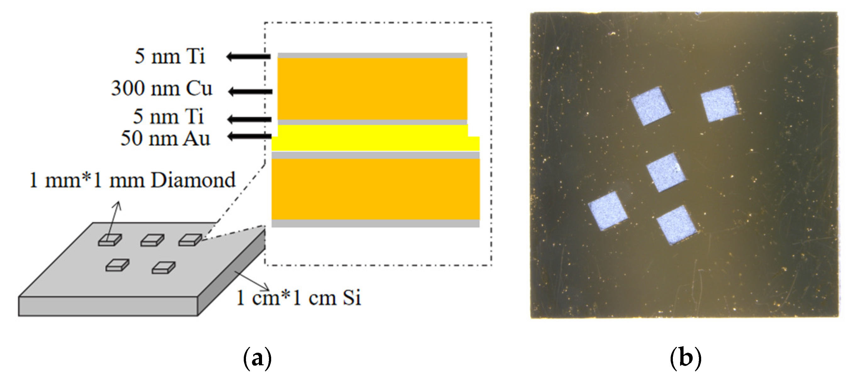
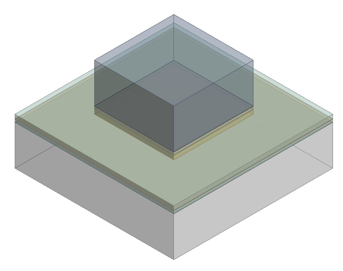
2.1. Sample Preparation

Firstly, the diamond (1 × 1 × 0.3 mm3) and silicon wafer (10 × 10 × 0.3 mm3) were ultrasonically cleaned in isopropyl alcohol, acetone, and ethanol for about 10 min and then rinsed with ultra-pure water. The residual liquid on the surface was blown dry using a nitrogen gun. Next, the electron beam evaporation coating machine (Oxford Vapour Station 4) was employed to deposit metal modification layers of Ti, Cu, Ti, and Au with thicknesses of 5, 300, 5, and 50 nm, respectively, onto the surfaces of both the diamond and silicon wafer. The resulting samples were referred to as Si-Ti/Cu/Ti/Au and D-Ti/Cu/Ti/Au, respectively. The process was carried out at 25 °C under a nitrogen atmosphere (10−5 Pa). Following the completion of thin-film deposition, samples were promptly removed from the deposition equipment and then subjected to room-temperature, low-pressure bonding using the Fineplacer Lambda-controlled chip bonder (bonding pressures of 1, 3, 5, and 6 MPa). The resulting bonding samples were denoted as Si-Ti/Cu/Ti/Au-D. Additionally, to assess surface roughness, Ti, Ti/Cu, Ti/Cu/Ti, and Ti/Cu/Ti/Au were deposited on the Si surface using a similar method as described above. These corresponding samples were denoted as Si-Ti, Si-Ti/Cu, Si-Ti/Cu/Ti, and Si-Ti/Cu/Ti/Au, respectively.

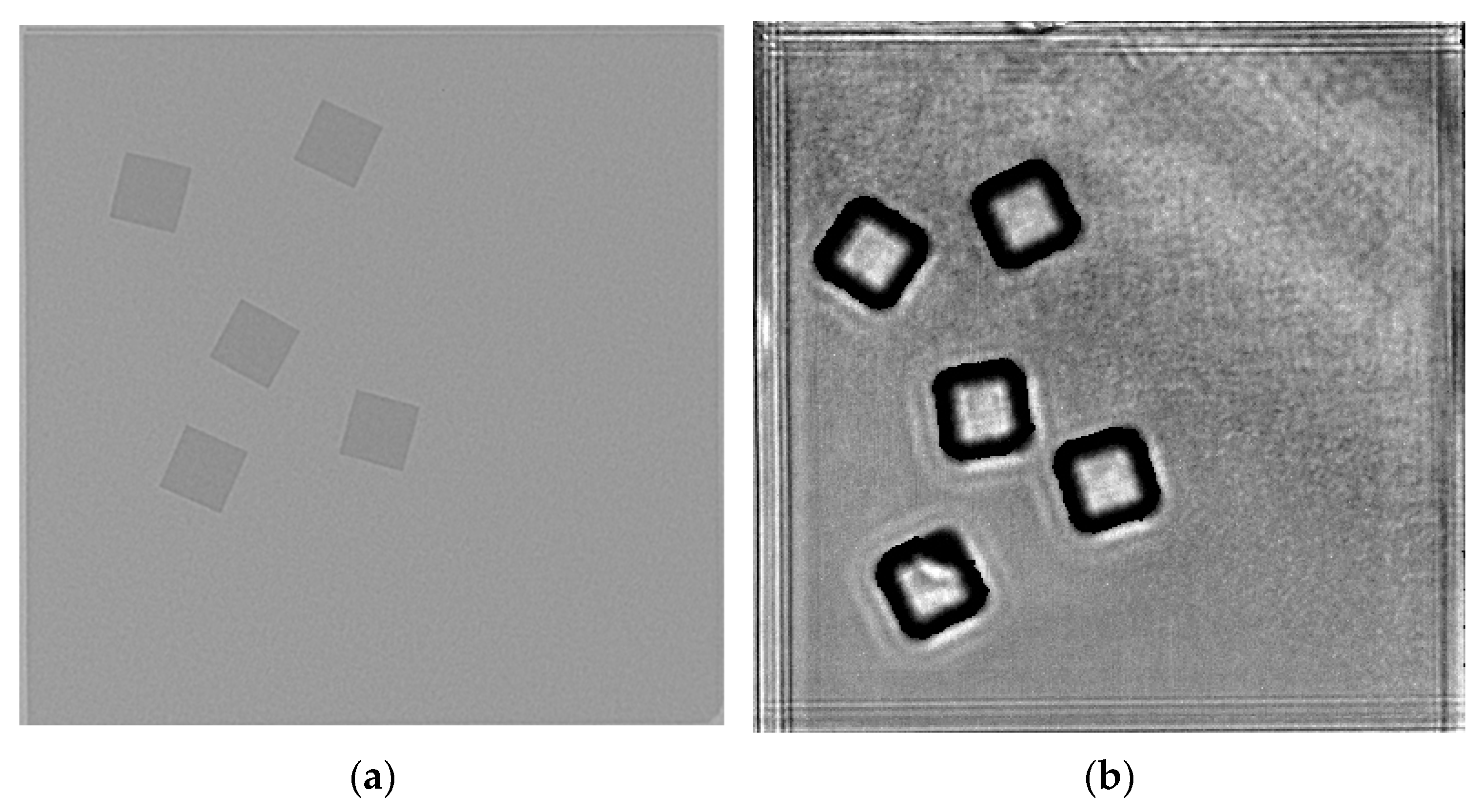
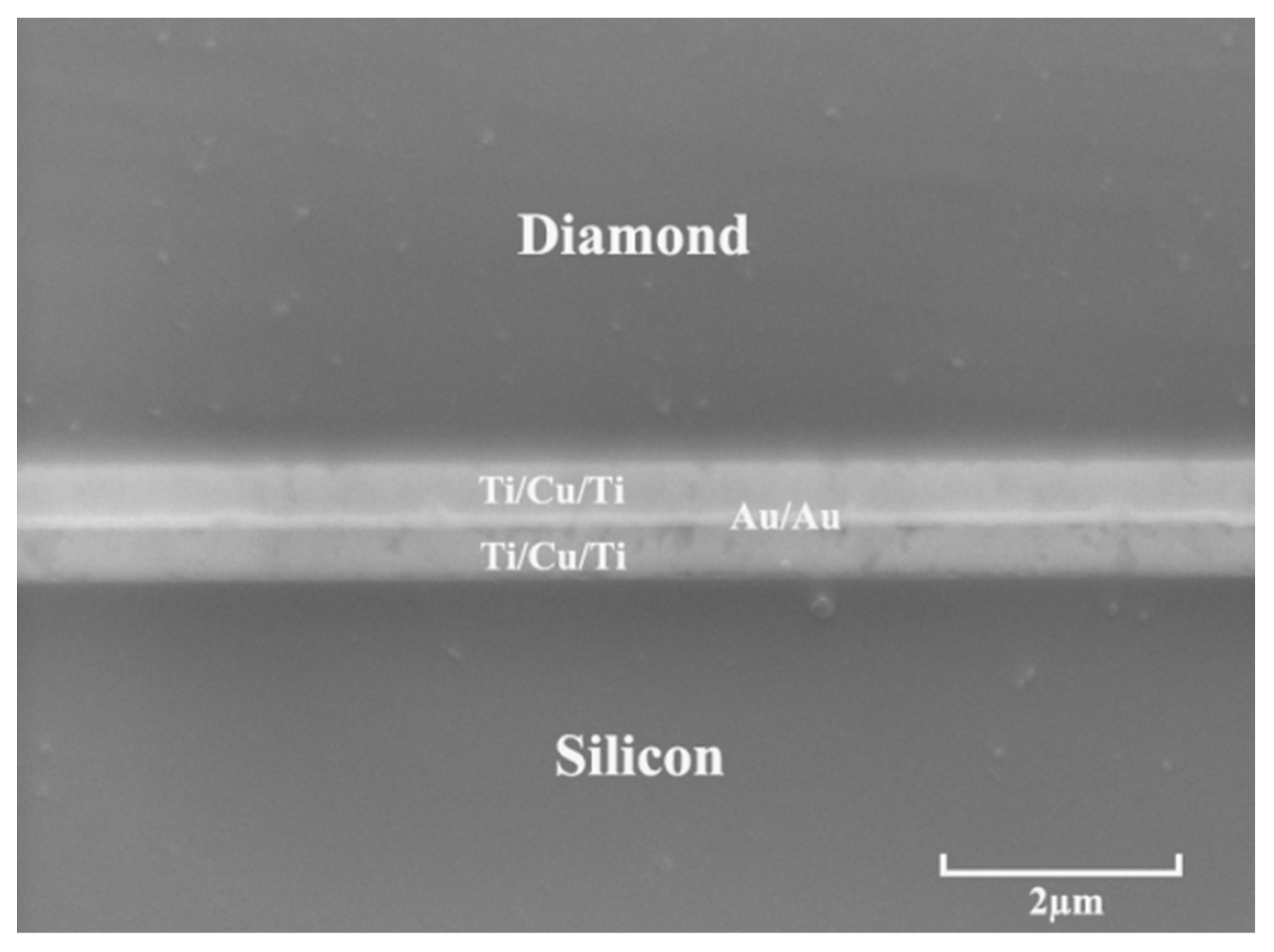
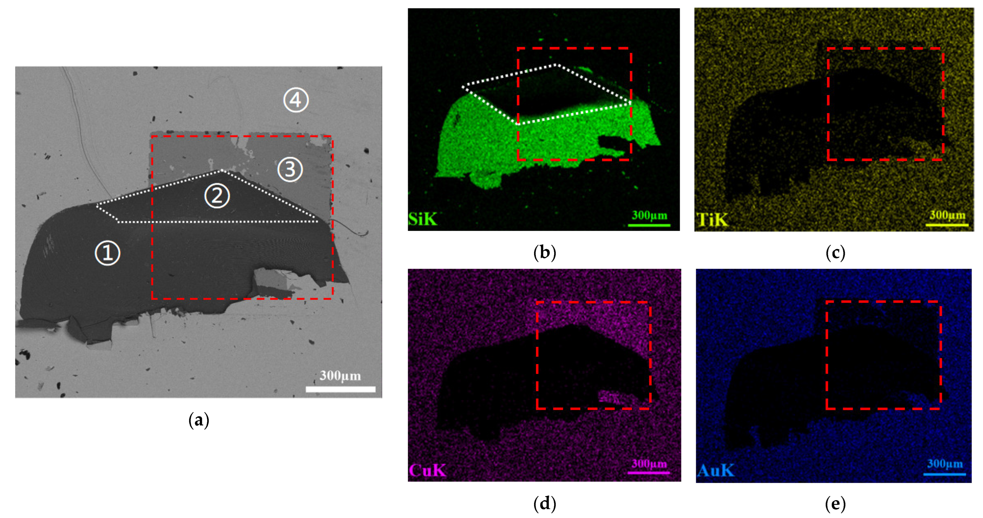
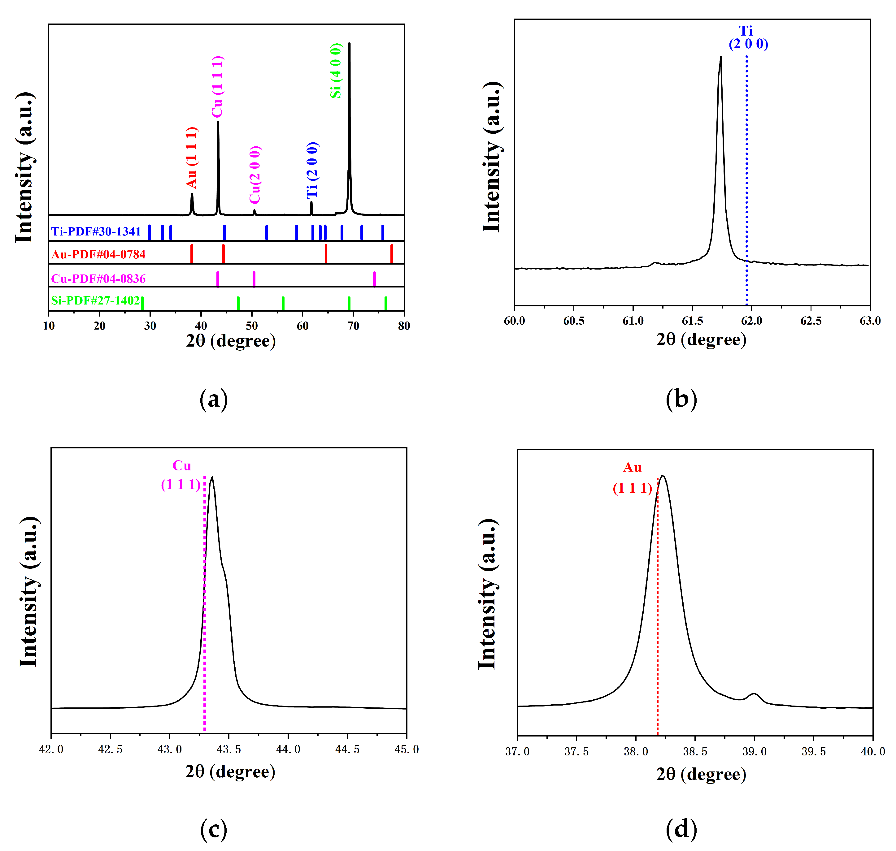
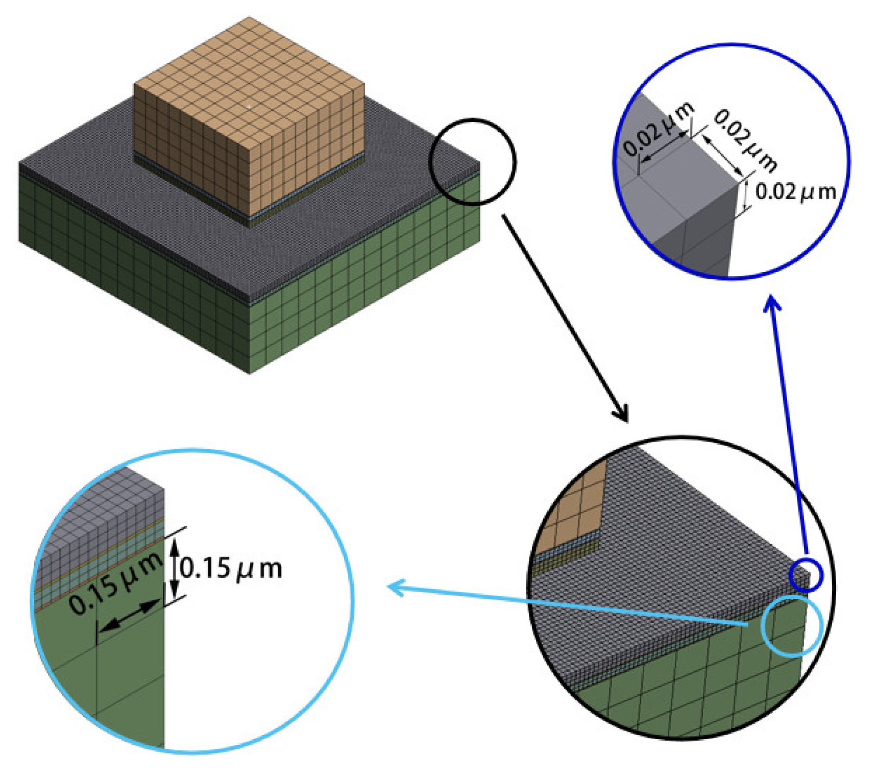
2.2. Characterizations

The surface morphologies of the samples were characterized via optical microscopy (Primo Star, Carl Zeiss AG, Jena, Germany), an ultra-depth of field stereo microscope (Nikon SMZ 18), and atomic force microscopy (AFM, Dimension ICON, Bruker, Billerica, MA, USA). X-ray diffraction (XRD) measurements (Rigaku Corporation, Tokyo, Japan) were performed on a Rigaku MinFlex600 diffractometer with Cu Kα radiation (λ = 1.54187 Å). The internal structures of the samples were observed using an X-ray inspection system (XD7600NT Ruby FP, Nordson DAGE, Aylesbury, UK) and acoustic scanning microscopy (SAM, D9500, SONOSCAN, Elk Grove Village, IL, USA). The cross-section and fracture surfaces were characterized for morphology and elemental distribution using a TESCAN MIRA3 scanning electron microscope (SEM, TESCAN, Brno, Czech Republic) and energy-dispersive spectroscopy (EDS). The shear force measurements on Si-Ti/Cu/Ti/Au-D samples, subjected to different bonding pressures, were conducted with an MFM1200 (DRY, Yantai, China) tensile shear force tester. The shear blade made contact with the bonded sample and applied a shear force parallel to the bonding interface. When the shear force reached the fracture threshold, the diamond layer was detached.

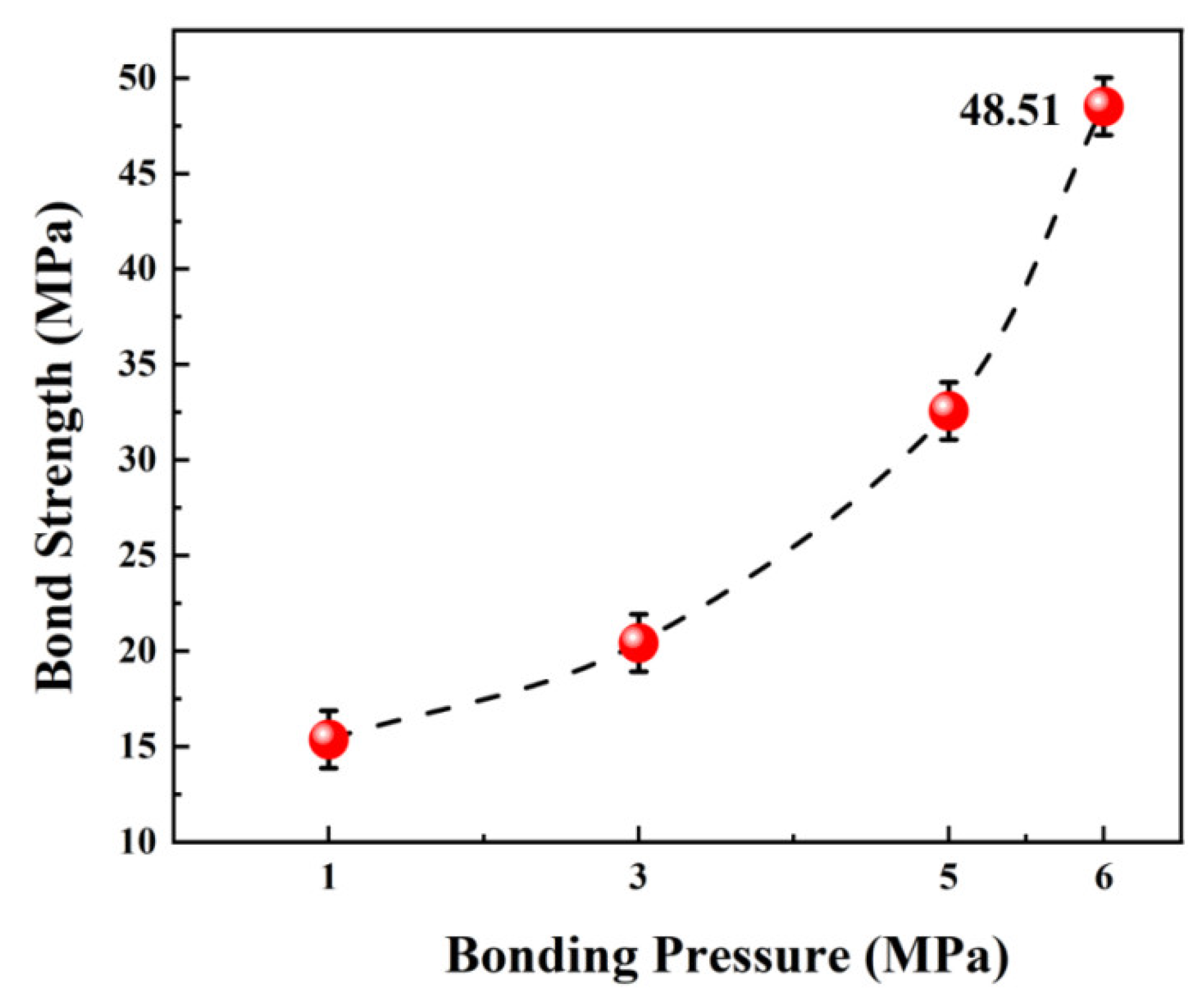
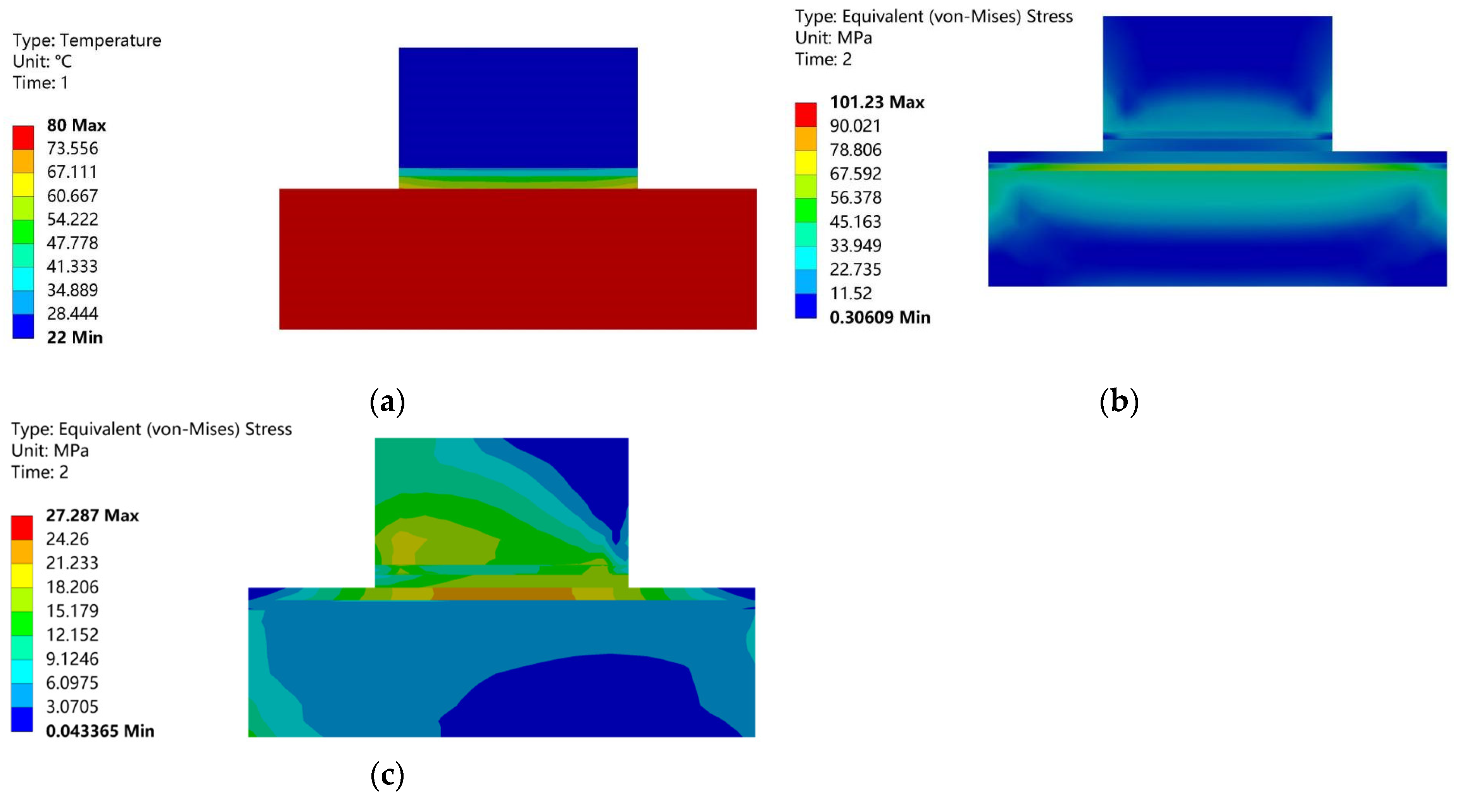
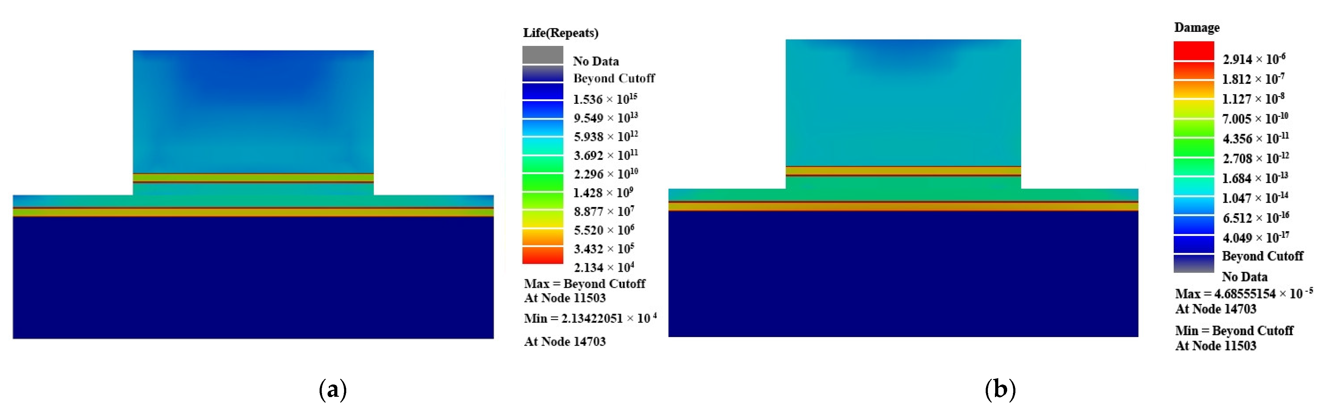
3. Results and Discussion

The specific process flow is illustrated in Figure 1. Ti/Cu/Ti/Au films on the cleaned silicon and diamond surfaces, respectively, were evaporated. The samples were then placed in a bonding machine to bond the two sheets at room temperature. In order to save costs and conduct control experiments, we bonded five samples on each silicon wafer. Figure 2a is a schematic diagram of the bonding structure, and Figure 2b is a picture of the actual sample. Figure 3a, Figure 3b, Figure 3c, and Figure 3d depict optical microscopy images of Si-Ti, Si-Ti/Cu, Si-Ti/Cu/Ti, and Si-Ti/Cu/Ti/Au, respectively. As observed in the images, the surfaces of each deposited layer appear uniform without any defects or imperfections, indicating that the employed process conditions and environment effectively maintain the cleanliness of each deposition layer. Additionally, to assess the surface roughness of the samples, AFM images of the prepared Si-Ti (a, e), Si-Ti/Cu (b, f), Si-Ti/Cu/Ti (c, g), and Si-Ti/Cu/Ti/Au (d, h) samples are shown in Figure 4. Surface roughness refers to the unevenness of the surface with small spacing and tiny peaks and valleys, which is one of the determining factors of the quality of the bonding surface. It has been noted that there are only a few protrusions at the interface of the Ti/Cu/Ti (Figure 4c) thin film due to the uneven deposition of Ti atoms during the deposition process. Analysis of the thin-film surfaces using NanoScope Analysis 1.7 software reveals that the surface roughness increases from 0.52 nm to 2.17 nm with the increase in the number of deposition layers (Figure 4i). The surface of the diamond side has a similar roughness: ~0.56 nm, ~1.79 nm, ~2.21 nm, and ~2.23 nm in roughness of the D-Ti, D-Ti/Cu, D-Ti/Cu/Ti, and D-Ti/Cu/Ti/Au layers. These values are similar to the roughness reported in previous research and are suitable for the bonding requirements [21]. The X-ray measurement displays no apparent defects within the interior of the Si-Ti/Cu/Ti/Au-D bonding structure (Figure 5a). In the SAM image of Si-Ti/Cu/Ti/Au-D (Figure 5b), it is observed that there are black shadows at the edges of the bonded sample, attributed to strong acoustic wave reflection in the edge regions of the bonding. Furthermore, the sunken areas in the upper part of the samples change the reflection, refraction, or scattering of acoustic waves, also resulting in the appearance of black shadows. However, no voids, cracks, or defects were found in the middle sections of these samples, indicating good bonding quality. The Si-Ti/Cu/Ti/Au-D cross-section was exposed using a metallographic grinding method and observed by SEM. As shown in Figure 6, the film layers at the Si-Ti/Cu/Ti/Au-D bonding interface are compact, and no extensive defects such as large voids or delamination can be observed. Only tiny voids were detected in the lower Cu layer.
The bonding strength of Si-Ti/Cu/Ti/Au-D was evaluated using a tensile shear force tester. The strength test results (Figure 7) indicate that as the bonding pressure increases, the bonding strength also increases. When the bonding pressure reaches 6 MPa, the bonding strength reaches 48.51 MPa. Upon reaching the shear force fracture threshold, the diamond layer is detached. Figure 8a, Figure 8b, Figure 8c, and Figure 8d represent the fracture surface morphology for bonding pressures of 1, 3, 5, and 6 Mpa, respectively. In these images, the bright regions correspond to the fractured silicon substrate, with the fracture extending beyond the bonding area. It is worth noting that the thin film coatings at the bonding interface also underwent delamination. To delve further into the interface fracture mechanism, SEM observations of the cross-sectional morphology of the Si-Ti/Cu/Ti/Au-D sample bonded at 6 Mpa were conducted. Additionally, EDS analysis of element distribution was performed, as shown in Figure 9 (the red box highlights the bonding area). In Figure 9a, the elements in regions marked as ① and ② are primarily Si, which is the main component of the fracture surface. No other elements are detected in this region, indicating that the Si layer experiences brittle fracture under shear force. This also confirms that the bonding layer strength is greater than that of the substrate. In Figure 9b, the region corresponding to ② in Figure 9a appears black because the interface fracture is deeper, resulting in weaker signals produced by the interaction between the electron beam and the sample, which is difficult to detect. However, considering the overall analysis of the distribution of other elements, it can be concluded that Si is present in this region. In Figure 9a, the region labeled as ③ is primarily composed of Cu (Figure 9d) with a small amount of Ti (Figure 9c), indicating that, in addition to Si fracture, the Ti in the Ti/Cu interface also detaches under the action of shear force. The region ④ in Figure 9a is the non-bonding area, and its composition includes Ti (Figure 9c), Cu (Figure 9d), and Au (Figure 9e). The above analysis results show that the Ti and Cu surface diffused through the Au layer to the non-bonding interface, and Au was the element present at the bonding interface.
As mentioned above, the Si-Ti/Cu/Ti/Au-D bonding structure exhibits reliability issues at the Si/Ti and Ti/Cu interfaces under shear force. It is reasonable to speculate that the decrease in the strength of the Ti layer may be a potential cause of the failure. To clarify the influence of the Ti layer on the overall bonding structure, the XRD measurement was conducted on Si-Ti/Cu/Ti/Au-D. As shown in Figure 10, the XRD spectra of the Si (400) [22], Au (111) [23], Cu (111), and Cu (200) [24] crystal planes closely match the crystal structure data from standard PDF cards. The positions of the strongest diffraction peaks of Cu and Au are not significantly shifted. However, the diffraction peak for the Ti (200) [25] crystal plane exhibits a low-intensity and approximately 0.3° shift towards lower angles. This may be attributed to the fact that dislocation growth, caused by the mismatch between the thin Ti layer (only about 5 nm) and the lattice interface of Cu, Si, and Au, cannot be completely eliminated through the formation of the transition layer, and that the interface stress cannot be effectively released. On the other hand, the difference in the lattice parameters of the metal layers above and below the Ti layer (as shown in Table 1) also causes the direction of the interface dislocation stress on the Ti layer to be inconsistent, further aggravating the lattice distortion inside the Ti layer [26]. Additionally, the thermal expansion of the Cu layer exerts compressive forces on the Ti layer, exacerbating the distortion behavior of the lattice structure of the Ti layer. Ultimately, the lowest strength in the Ti/Cu/Ti/Au metal modification layer structure makes the Ti layer the weakest link in terms of mechanical reliability.
The finite element-based, thermo-mechanical fatigue analysis method involves creating an analysis model based on the material’s fatigue performance parameters and the load history applied to the structural component [27]. This method utilizes finite element analysis to establish the model, requiring the construction of a finite element model, determination of material parameters, and design of the load. This yields stress and strain results for the structural model. Subsequently, these results are input into fatigue analysis software, where a combined thermal–mechanical load is constructed. Using the material’s fatigue performance parameters and applying the necessary fatigue criteria, the software calculates the fatigue life for each load cycle. Finally, the cumulative damage theory is employed to calculate the overall structural fatigue life [28]. It is worth noting that, due to the often complex stress states in structures, and the fact that the S-N curves for structural materials are typically obtained under simple stress conditions in experiments, the commonly used minimum energy yield criterion or other equivalent criteria are employed to replace the complex stresses at the studied fatigue points with equivalent stresses. For finite element analysis, this process is readily achievable. Once the equivalent substitution is made, a fatigue life assessment can be carried out with reference to the original material’s S-N curve. This approach does not strictly differentiate between crack initiation and crack propagation but provides an overall lifetime estimation for the structure prior to failure.
Based on the nominal stress method [29], the coupled thermal–mechanical analysis was conducted using ANSYS Mechanical finite element software, along with the nCode DesignLife fatigue analysis module, to elucidate the mechanical performance and potential failure points of the Si-Ti/Cu/Ti/Au-D structure. Figure 11 represents the simulation model, and the material properties of each layer are listed in Table 2. Due to significant differences in structural dimensions, the simulation model is simplified. As shown in Figure 12, the refined meshes are applied to the metal layers (divided into 0.02 × 0.02 × 0.02 µm3), while standard mesh divisions are used for the silicon substrate and diamond (divided into 0.15 × 0.15 × 0.15 µm3). Contact bonding is established between the various components.
Therefore, the temperature distribution of the chip should be simulated when it is working. The temperature of the Si and diamond blocks is set to 80 °C and 22 °C, respectively, and the remaining surfaces are assigned a convective heat transfer coefficient of 5 × 10⁻⁶ W/mm2·K. The temperature distribution of the Si-Ti/Cu/Ti/Au-D structure is illustrated in Figure 13a. As can be seen in the figure, the temperature changes are mainly distributed in the bonding layer. In the first loading step, a thermal load is added to the mechanical module, for which the fixed supports are applied to the bottom surface, resulting in a distribution cloud map of thermal stress (Figure 13b). By observing the stress results in the static field, we found that the maximum thermal stress (101.23 MPa) in the Si-Ti/Cu/Ti/Au-D bonding structure is located in the interface between Cu and Ti due to the large thermal expansion coefficient (1.6 × 10⁻⁵ K−1) of Cu, resulting in stress concentration. The prolonged thermal stress could accelerate crack formation and potentially propagate toward the central bonding region, causing deformation and failure of the bonding layer structure [30]. The second loading step is mechanical stress analysis. To simulate shear stress, the compressive stress of 10 MPa is applied to the lateral surface of the diamond. At the same time, the fixed support boundary conditions are applied to the lower surface of the Si block to observe the stress distribution in the Si block. The equivalent stress cloud map results (Figure 13c) show that the equivalent stress is mainly concentrated in the metal layers under the action of 10 MPa shear stress, including the Ti, Au, and Cu layers. Particularly at the interface between Cu and Ti, the stress concentration is prominent, indicating that the bonding interface between Cu and Ti in the Si-Ti/Cu/Ti/Au-D bonding structure is the weak point, prone to damage under shear stress, and could potentially lead to the failure of the entire bonding structure.
Fatigue analysis was performed next, starting with the construction of a fatigue stress spectrum. The construction of a fatigue stress spectrum involves load mapping. Fatigue damage arises from pulsating stresses, and finite element analysis provides stress and strain results at specific solution points. To calculate fatigue damage, it is necessary to apply stress/strain histories. Load mapping transforms finite element results into stress/strain histories for use in fatigue calculations. Traditional finite element analysis software can only apply single loads and does not provide alternating loads. To address this issue, an effective method is required to combine the thermal stress analysis results with stresses from other sources. Ncode DesignLife utilizes a Hybrid Load Provider to generate alternating load histories by combining temperature and stress. Constant amplitude loading is the simplest form of load mapping, assuming cyclic variation in stress/strain between maximum and minimum values and a linear correlation between stress/strain and load. During the solving process, it is necessary to configure the solver to comprehensively consider various factors that influence the structural fatigue life and enhance the analysis’s reliability [31]. In nCode Design Life, setting up temperature effects is a crucial step, accomplished through enabling the impact of temperature on the components. Modifications to the solver settings include using the Multi-Temperature Cures analysis method, employing the Rainflow counting Critical Plane approach for stress combination, applying the Goodman mean stress correction method, setting the survival probability to 90%, and using a safety factor of 1, while leaving the rest at default settings.
In this study, constant amplitude loading was employed, using the Hybrid Load Provider to construct a load spectrum combining thermal stress, shear forces, and temperature loads. The results of temperature stress and shear stress were imported into nCode DesignLife software, corresponding S-N curves were added for each material, and the Hybrid Load Provider method was used to simulate the alternating load of temperature and thermal stress [32]. Following reliability virtual fatigue analysis [33], the cloud maps of fatigue life and cumulative fatigue damage of the Si-Ti/Cu/Ti/Au-D structure are shown in Figure 14. Based on the fatigue life plot in Figure 14a, the minimum life is 21,340 cycles. As depicted in the fatigue damage cloud plot in Figure 14b, the earliest occurrence of fatigue failure in the Si-Ti/Cu/Ti/Au-D structure is located within the Ti layer.

4. Conclusions

Utilizing electron beam evaporation and room-temperature, low-pressure bonding processes, the Ti/Cu/Ti/Au metal modification layer effectively affixes the diamond onto the silicon substrate. The surface of each coating is uniform, with low roughness values and without defects. The Si-Ti/Cu/Ti/Au-D bonding structure exhibits no delamination, and the internal layers within the bonding layer are dense, indicating a high overall bonding quality. Mechanical performance testing and analysis reveal that the bonding strength increases with higher bonding pressure, reaching 48.51 MPa at 6 MPa. Under shear forces, the bulk silicon exhibits pronounced brittle fracture characteristics, while the presence of Cu and Ti at the interface indicates that the fracture also occurs at the Ti/Cu interface. The XRD analysis shows that there is serious lattice expansion distortion in the Ti layer, resulting in the lowest strength at the surface. The simulation results demonstrate that the fatigue damage primarily occurs within the Ti layer under thermomechanical coupled loads, which is because the thermal expansion of the Cu layer exerts compression on both the upper and lower Ti layers, leading to damage accumulation and ultimately reducing the strength of the Ti layer. The failure risk points of the Si-Ti/Cu/Ti/Au-D bonding structure revealed by the experimental and simulation results have practical significance for further optimizing the bonding process and enhancing the stability of the bonding structure.

Author Contributions

Conceptualization, M.Z. and X.J.; methodology, M.Z., X.J., S.C., X.L. and X.Y.; software, M.Z., X.J. and T.G.; validation, M.Z., X.J. and X.L.; formal analysis, M.Z., X.J. and X.L.; investigation, M.Z., X.J. and Y.T.; resources, X.J., S.C., M.C., G.W., Z.Z. and X.Y.; data curation, M.Z., X.J. and X.L.; writing—original draft preparation, M.Z., X.J. and X.L.; writing—review and editing, M.Z., X.J. and X.L.; visualization, M.Z., X.J., M.C., G.W. and Z.Z.; supervision, M.Z., X.J., S.C., X.L. and X.Y.; project administration, X.J., S.C. and X.Y.; funding acquisition, X.J. and X.Y. All authors have read and agreed to the published version of the manuscript.

Funding

This research was funded by Guangzhou Science and Technology Project Fund (No. 202201011247) and the Natural Science Foundation of Fujian Province of China (No. 2022J011264).

Data Availability Statement

Data are contained within the article.

Conflicts of Interest

The authors declare no conflict of interest.

References

  1. Venkateswarlu, S.; Mishra, S.; Oprins, H.; Vermeersch, B.; Brunion, M.; Han, J.H.; Stan, M.R.; Biswas, D.; Weckx, P.; Catthoor, F. Impact of 3-D Integration on Thermal Performance of RISC-V MemPool Multicore SOC. In IEEE Transactions on Very Large Scale Integration (VLSI) Systems; IEEE: Piscataway, NJ, USA, 2023; pp. 1–9. [Google Scholar] [CrossRef]
  2. Abdullah, M.F.; Mat Hussin, M.R.; Ismail, M.A.; Wan Sabli, S.K. Chip-level thermal management in GaN HEMT: Critical review on recent patents and inventions. Microelectron. Eng. 2023, 273, 111958. [Google Scholar] [CrossRef]
  3. Martin, H.; Reintjes, M.; Reijs, D.; Dorrestein, S.; Kengen, M.; Libon, S.; Smits, E.; Tang, X.; Koelink, M.; Poelma, R.; et al. Heterogeneous Integration of Diamond Heat Spreaders for Power Electronics Application. In Proceedings of the 2023 IEEE 73rd Electronic Components and Technology Conference (ECTC), Orlando, FL, USA, 30 May–2 June 2023; IEEE: New York, NY, USA, 2023; pp. 118–125. [Google Scholar]
  4. Xin, J.; Junjun, W.; Yabo, H. Application progress of diamond heat dissipation substrate in GaN-based power devices. Surface Technol. 2020, 49, 120–132. [Google Scholar]
  5. Anupam, K.C.; Anderson, J.; Ayala, A.; Engdahl, C.; Piner, E.L.; Holtz, M.W. Heterogeneous integration of high-quality diamond on aluminum nitride with low and high seeding density. J. Cryst. Growth 2023, 610, 127172. [Google Scholar] [CrossRef]
  6. Minoura, Y.; Ohki, T.; Okamoto, N.; Yamada, A.; Makiyama, K.; Kotani, J.; Ozaki, S.; Sato, M.; Nakamura, N. Surface activated bonding of SiC/diamond for thermal management of high-output power GaN HEMTs. Jpn. J. Appl. Phys. 2020, 59, SGGD03. [Google Scholar] [CrossRef]
  7. Kwak, T.; Lee, J.; Choi, U.; So, B.; Yoo, G.; Kim, S.; Nam, O. Diamond Schottky barrier diodes fabricated on sapphire-based freestanding heteroepitaxial diamond substrate. Diam. Relat. Mater. 2021, 114, 108335. [Google Scholar] [CrossRef]
  8. Kim, S.-W.; Takaya, R.; Hirano, S.; Kasu, M. Two-inch high-quality (001) diamond heteroepitaxial growth on sapphire (1120) misoriented substrate by step-flow mode. Appl. Phys. Express 2021, 14, 115501. [Google Scholar] [CrossRef]
  9. Ahmed, R.; Siddique, A.; Anderson, J.; Gautam, C.; Holtz, M.; Piner, E. Integration of GaN and diamond using epitaxial lateral overgrowth. ACS Appl. Mater. Interfaces 2020, 12, 39397–39404. [Google Scholar] [CrossRef]
  10. Ling, B.; Jing, N.; Jincheng, Z.; Dong, W.; Boyu, W.; Haidi, W.; Jianglin, Z.; Ran, T.; Zhonghui, L. Van der waals epitaxial GaN thin films on polycrystalline diamond substrate. J. Synth. Cryst. 2023, 52, 901–908. [Google Scholar] [CrossRef]
  11. Caoyuan, M.; Genzhuang, L.; Wenliang, X.; Qiliang, W.; Xianyi, L.; Liu’an, L.; Guangtian, Z. Research progress in preparation of large size single crystal diamond by microwave plasma chemical vapor deposition. Electron. Packag. 2023, 23, 36–45. [Google Scholar] [CrossRef]
  12. Wenqiang, X. A Study of Nitride Epitaxy and Properties on Diamond Substrates. Master’s Thesis, Xidian University, Xi’an, China, 2022. [Google Scholar]
  13. Srimurugan, R.; Vijay Ananth, S.; Geethan, A.; Jayaseelan, V.; Xavier, J.F. Experimental investigation on diffusion bonding of dissimilar metals. AIP Conf. Proc. 2020, 2283, 020062. [Google Scholar] [CrossRef]
  14. Matsumae, T.; Kurashima, Y.; Umezawa, H.; Mokuno, Y.; Takagi, H. Room-temperature bonding of single-crystal diamond and Si using Au/Au atomic diffusion bonding in atmospheric air. Microelectron. Eng. 2018, 195, 68–73. [Google Scholar] [CrossRef]
  15. Matsumae, T.; Kurashima, Y.; Takagi, H. Surface activated bonding of Ti/Au and Ti/Pt/Au films after vacuum annealing for MEMS packaging. Microelectron. Eng. 2018, 197, 76–82. [Google Scholar] [CrossRef]
  16. Fei, W.; Kang, W.; Genqiang, C.; Fang, L.; Ruozhen, W.; Wei, W.; Minghui, Z.; Wenbo, H.; Hongxing, W. Room temperature bonding of diamond/Si with Mo/Au interlayers in atmospheric air. Diam. Relat. Mater. 2023, 135, 109844. [Google Scholar] [CrossRef]
  17. Shimatsu, T.; Uomoto, M.; Oba, K.; Furukata, Y. Atomic diffusion bonding of wafers in air with thin Au films and its application to optical devices fabrication. In Proceedings of the 2012 3rd IEEE International Workshop on Low Temperature Bonding for 3D Integration, LTB-3D 2012, Tokyo, Japan, 22–23 May 2012; p. 103. [Google Scholar]
  18. Zeguang, L.; Dengquan, C.; Ximing, L.; Kun, X. Gold-tin alloy solder for the package of microelectronics. Precious Met. 2005, 26, 62–65. [Google Scholar]
  19. Bao, S.; Zhong, Y.; He, Y.; Li, K.; Yu, D. Low-temperature die to glass wafer bonding based on Au-Au atomic diffusion. In Proceedings of the 2022 China Semiconductor Technology International Conference (CSTIC), Shanghai, China, 20–21 June 2022; pp. 1–3. [Google Scholar]
  20. Guo, C.; Fangyuan, S.; Jialiang, D.; Zifan, C.; Xitao, W.; Jinguo, W.; Kim, M.J.; Hailong, Z. Effect of Ti interlayer on interfacial thermal conductance between Cu and diamond. Acta Mater. 2018, 160, 235–246. [Google Scholar] [CrossRef]
  21. Higurashi, E.; Okumura, K.; Kunimune, Y.; Suga, T.; Hagiwara, K. Room-temperature bonding of wafers with smooth au thin films in ambient air using a surface-activated bonding method. IEICE Trans. Electron. 2017, E100C, 156–160. [Google Scholar] [CrossRef]
  22. Sukkurji, P.A.; Issac, I.; Singaraju, S.A.; Velasco, L.; Hagmann, J.A.; Bessler, W.; Hahn, H.; Botros, M.; Breitung, B. Tailored silicon/carbon compounds for printed Li–Ion anodes. Batter. Supercaps 2020, 3, 713–720. [Google Scholar] [CrossRef]
  23. Xuefeng, R.; Ying, S.; Anmin, L.; Jie, Z.; Peixia, Y.; Jinqiu, Z.; Maozhong, A. Experimental and theoretical studies of DMH as a complexing agent for a cyanide-free gold electroplating electrolyte. RSC Adv. 2015, 5, 64997–65004. [Google Scholar] [CrossRef]
  24. Dongsheng, W.; Mingyue, F.; Tingyu, H.; Fanming, Z.; Xiaoli, H.; Li, C.; Zhongmin, S. Cu/CuxS-embedded N,S-doped porous carbon derived in situ from a MOF designed for efficient catalysis. Chem. Eur. J. 2021, 27, 11468–11476. [Google Scholar] [CrossRef]
  25. Mohaghegh, F.; Akhbari, K.; Phuruangrat, A. Preparation of thallium nanomaterials from thallium(I) coordination polymers precursors synthesized by green sonochemical and mechanochemical processes. Ultrason. Sonochem. 2018, 40, 594–600. [Google Scholar] [CrossRef]
  26. Goldfarb, I.; Pelleg, J.; Zevin, L.; Croitoru, N. Lattice distortion in thin films of IVB metal (Ti, Zr, Hr) nitrides. Thin Solid Films 1991, 200, 117–127. [Google Scholar] [CrossRef]
  27. Tenghiri, L.; Khalil, Y.; Abdi, F.; Bentamy, A. Structural design and analysis of a small wind turbine blade using Simple Load Model, FAST-MLife codes, and ANSYS nCode DesignLife. Wind Eng. 2019, 45, 0309524X1988243. [Google Scholar] [CrossRef]
  28. Sivachev, S.; Myagkov, L. Thermomechanical fatigue analysis of diesel engine piston: Finite element simulation and lifetime prediction technique. In Proceedings of the 5th International Conference on Industrial Engineering (ICIE 2019), Sochi, Russia, 25–29 March 2019; Volume I 5, pp. 109–117. [Google Scholar]
  29. Xianming, L.; Zheng, H.; Bo, W.; Zhilin, L.; Lei, L.; Chongjun, H.; Feng, G. Fatigue life analysis on hydraulic end of fracturing pump based on nCode DesignLife. China Pet. Mach. 2023, 51, 90–96. [Google Scholar] [CrossRef]
  30. Pengfei, C. Research on Thermal Fatigue of Electric Connectors. Master’s Thesis, Beijing University of Posts and Telecommunications, Beijing, China, 2022. [Google Scholar]
  31. Sener, A.S. Fatigue life evaluation of an electrically driven shuttle frame using finite element analysis. Mater. Test. 2021, 63, 329–335. [Google Scholar] [CrossRef]
  32. Xiangyu, C.; Qingyu, L.; Wenzhen, L.; Fan, Y.; Tingting, H. Research about thermal fatigue characteristic of IGBT module in considering of electrothermal-mechanism coupling and crack. Smart Grid 2017, 7, 443–451. [Google Scholar]
  33. Lifeng, G.; Ruijing, Z.; Liguo, L.; Hui, G.; Jianping, X. Fatigue reliability analysis for the mechanical system of large-scale medical imaging equipment SPECT. In Proceedings of the 2018 2nd International Conference on Advances in Energy, Environment and Chemical Science (AEECS 2018), Zhuhai, China, 2–4 February 2018; pp. 168–172. [Google Scholar]
Figure 1. The schematic diagram of the Si-Ti/Cu/Ti/Au-D preparation process.
Crystals 13 01625 g001
Figure 2. The schematic diagram of the Si-Ti/Cu/Ti/Au-D structure (a); photograph of the Si-Ti/Cu/Ti/Au-D samples (b).
Crystals 13 01625 g002
Figure 3. The optical microscope images of evaporated layer surface of Si-Ti (a), Si-Ti/Cu (b), Si-Ti/Cu/Ti (c), Si-Ti/Cu/Ti/Au (d).
Crystals 13 01625 g003
Figure 4. The AFM measurement results and surface roughness analysis (i) of Si-Ti (a,e), Si-Ti/Cu (b,f), Si-Ti/Cu/Ti (c,g), and Si-Ti/Cu/Ti/Au (d,h).
Crystals 13 01625 g004
Figure 5. The X-ray (a) and SAM (b) images of Si-Ti/Cu/Ti/Au-D.
Crystals 13 01625 g005
Figure 6. The SEM image of Si-Ti/Cu/Ti/Au-D cross-section.
Crystals 13 01625 g006
Figure 7. The bond strength at different bonding pressures.
Crystals 13 01625 g007
Figure 8. The ultra-depth of field stereo microscope images of the fracture surface at the bonding pressure of 1 (a), 3 (b), 5 (c), and 6 (d) MPa.
Crystals 13 01625 g008
Figure 9. The SEM (a) and EDS ((b) Si, (c) Ti, Cu (d), Au (e)) diagram of the fracture surface at 6 MPa bonding pressure of the Si-Ti/Cu/Ti/Au-D.
Crystals 13 01625 g009
Figure 10. The XRD pattern of the Si-Ti/Cu/Ti/Au-D (a), Ti offset (b), Cu offset (c), and Au offset (d).
Crystals 13 01625 g010
Figure 11. The diagram of the bonding structure model of the Si-Ti/Cu/Ti/Au-D.
Crystals 13 01625 g011
Figure 12. The mesh division of the Si-Ti/Cu/Ti/Au-D: the Ti/Cu/Ti/Au film layer size is divided into 0.02 × 0.02 × 0.02 µm3, and diamond and Si are divided into default mesh sizes (0.15 × 0.15 × 0.15 µm3).
Crystals 13 01625 g012
Figure 13. The temperature distribution diagram (a), the thermal stress distribution image (b), and the equivalent stress cloud image of the Si-Ti/Cu/Ti/Au-D (c).
Crystals 13 01625 g013
Figure 14. The fatigue life (a) and cumulative fatigue damage cloud maps (b) of Si-Ti/Cu/Ti/Au-D.
Crystals 13 01625 g014
Table 1. The crystallographic parameters.
ElementCrystal
Structure
a-Axis Lattice
Constant (Å)
c-Axis Lattice Constant (Å)Plane Spacing (Å)
SiFCC5.430-1.357 (4 0 0)
TiHCP3.4565.5251.496 (2 0 0)
CuFCC3.615-2.088 (1 1 1)
AuFCC4.078-2.355 (1 1 1)
Table 2. Material properties of the Si-Ti/Cu/Ti/Au-D.
Material PropertiesMaterial Name
SiTiCuAuDiamond
Density (kg/m−3)23304500893319,3003510
Elastic modulus (GPa)190102.0411078.51000
Poisson’s ratio0.27820.30.340.420.2
Thermal expansion coefficient (k−1)2.5 × 10−67.6 × 10−61.6 × 10−51.4 × 10−51.2 × 10⁻¹²
Thermal conductivity (W/m·K)148214003152000
Disclaimer/Publisher’s Note: The statements, opinions and data contained in all publications are solely those of the individual author(s) and contributor(s) and not of MDPI and/or the editor(s). MDPI and/or the editor(s) disclaim responsibility for any injury to people or property resulting from any ideas, methods, instructions or products referred to in the content.

