1. Introduction
With the swift advancement of modern science and technology, microelectronics has become an inextricable component, gaining increased importance. The level of development of microelectronics corresponds with a country’s overall strength and is presently one of the foremost industries in the world. The modern microelectronics industry has evolved into three distinct sectors: design, manufacturing, and encapsulation [
1]. Microelectronic encapsulation is now a key technology for the IT industry’s development and an essential component of the microelectronics industry. The primary purpose of microelectronic encapsulation technology is to assemble tens of thousands of semiconductor electronic components into a compact package that can receive power and exchange information with the external environment [
2]. However, electronic encapsulation devices are widely used in various fields, including communication satellites, automotive electronics, medical devices, and consumer electronics. As a result, they are vulnerable to various external environmental loads during production and service, such as residual stress, surface strain, chemical corrosion, electromigration caused by ambient humidity or current density, physical impact, and random vibration factors [
3]. The failure of electronic encapsulation devices can be caused by a combination of factors. To ensure their normal function and stability, a comprehensive analysis needs to be conducted, considering the materials, structure, and process. This will help to reduce the risk of device failure and improve reliability.
Since the 1990s, semiconductor technology has continuously developed and integrated, resulting in an increase in the number of pins on a chip. However, traditional pin socket technology has been unable to fulfil the need for high-density interconnections [
4]. Consequently, pin-less encapsulation technologies such as Ball Grid Array (BGA) have been introduced. BGA is an electronic encapsulation method known for connecting a chip’s pins to a grid of small balls, allowing for high-density micro-interconnections. Various types of BGA encapsulation are available on the market, differing in terms of substrate materials such as PBGA (plastic), CBGA (ceramic), CCGA (ceramic column arrays), and MBGA (metal) [
5,
6]. Each type of BGA encapsulation has its own characteristics and advantages in industrial applications.
Ceramic materials are preferred as they offer excellent properties, including good abrasion resistance, insulating properties, and thermal stability, making them an important material for microelectronic components [
7]. Ceramic Ball Grid Array (CBGA) is a type of BGA encapsulation that employs ceramic materials. It has excellent electrical properties, high-density integration, good airtightness, moisture resistance, and effective soldering performance. Due to its remarkable reliability, CBGA is widely utilized in national defense, military, and aerospace sectors, as well as other high-precision special equipment fields.
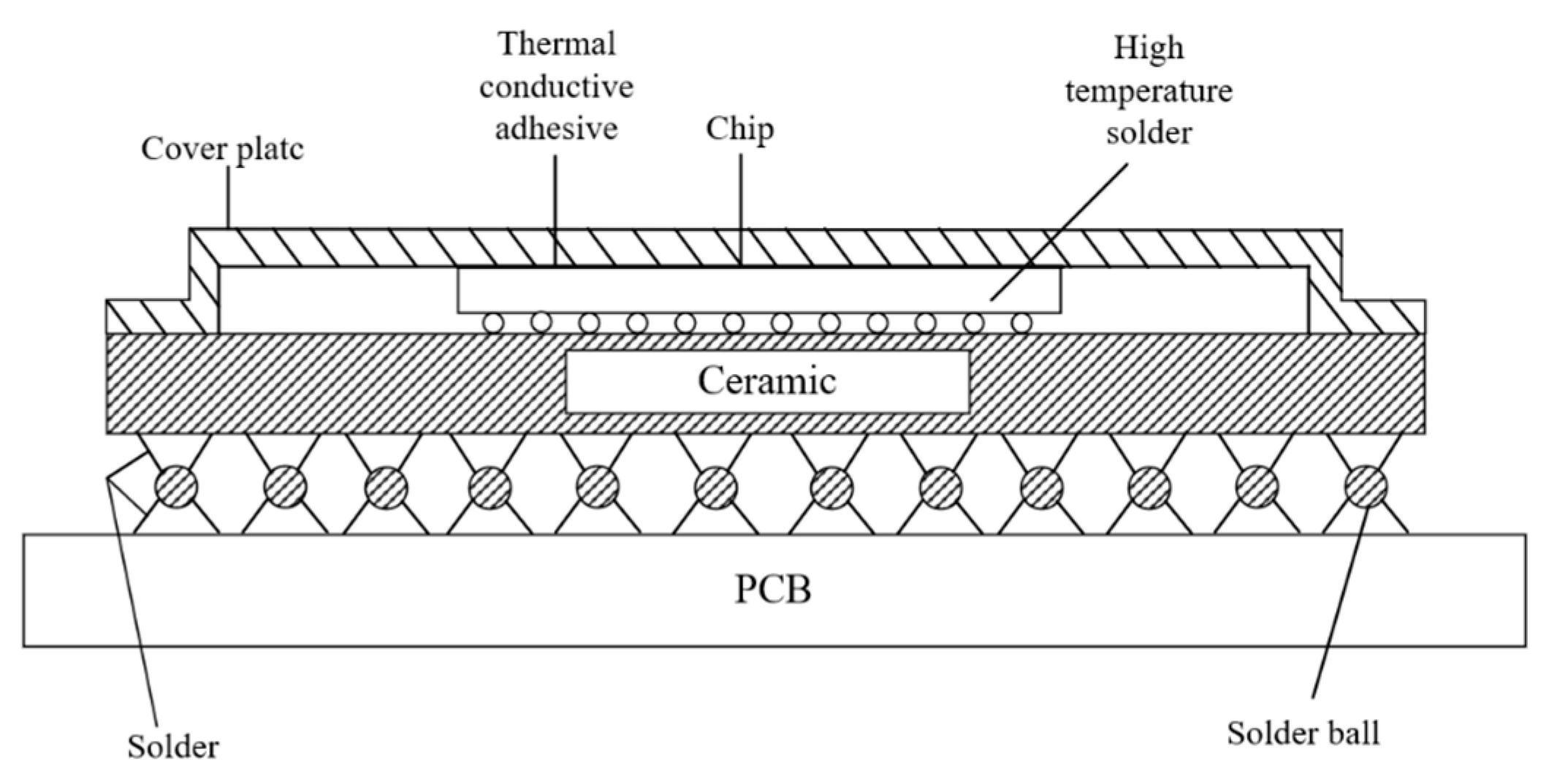
Figure 1 illustrates the typical encapsulation structure of CBGA [
8,
9].
In general, there are two primary reasons for electronic device failure: low-cycle thermal fatigue from temperature loading and high-cycle mechanical fatigue resulting from shock drops, vibration, and other loads [
10]. Based on statistical data published by the US military, 55% and 20% of electronic device failures were attributed to temperature loading and shock and vibration, correspondingly, as depicted in
Figure 2 [
11]. Most electronic device failures are caused by the malfunction of crystal structures in materials, such as solder balls and columns. Therefore, it is necessary to investigate the mechanical properties and failure mechanisms of these crystal structures when they are subjected to thermal loading. This research will facilitate the study of their performance and reliability.
During the welding process, the impact of temperature fluctuations on the crystal structures of electronic device materials is primarily demonstrated by the following factors: due to the large thermal expansion coefficient of the material’s constituent parts, the crystal structures itself experiences residual stress and thermal deformation during device cooling contraction. This, in turn, causes mismatched thermal stress between the constituent materials, increasing the stress and strain experienced by critical nodes in the crystal structures during subsequent service, and ultimately leading to deformation [
12,
13].
Figure 3 illustrates problems, including solder joint cracking and fracture, caused by temperature that significantly impede the reliable and safe operation of electronic equipment. Electronic device failure problems are a serious concern that must be addressed.
Wang and colleagues conducted research on the structure and thermal fatigue properties of solderless solder joints in ceramic ball array packaging (CBGA) structures through thermal cycling experiments and finite element modeling while sweeping the electrical observation point cross-section [
14]. Li and colleagues utilized the ANSYS software for finite element analysis to simulate stress and strain distribution and plastic work accumulation in the solder ball array of the CBGA packaging device. The reliability of the solder joints was then examined from the perspective of thermal cycling damage using Darveaux’s plastic energy accumulation damage equation. Lastly, a comparison was made between the performance of the single-solder-joint-array device and the composite-solder-joint-array packaging device [
15]. Lv et al. investigated the failure mechanism of surface-mounted solder joints at the board level of CBGA ball-implanted devices under cyclic loading conditions within a temperature range from −55 to 105 °C. The authors’ objective was to understand the relations between temperature, loading cycles, and solder joint reliability. The study results indicated that the key areas of failure in the solder joints of surface-mounted CBGA devices were the interfaces between the solder and ceramic ball, and the interfaces between solder joints and pads on two locations. In addition, there was a preference for the fracture of edge solder joints, which was a critical finding in failure analysis. Furthermore, the inboard link’s breakage failures occurred sequentially as the cyclic cycle increased [
16]. According to Guo’s test results, a high level of straight-through rate is achievable in the electronic assembly of CBGA through reasonable process design and management. Device defects and other factors primarily cause soldering defects. The overall reliability is dependent on the weakest link, and process control must prioritize addressing the weak link [
17]. Wang et al. used CBGA256 and CBGA500 circuit packages as examples to investigate the effects of ceramic shell quality on the quality of the CBGA ball planting process. They examined three aspects: pad coplanarity, positional accuracy, and ceramic surface flatness [
18].
In this paper, we analyze the residual stress of different parts of crystal structures of electronic device materials following exposure to high temperatures using experimental tests and finite element simulations. X-ray diffraction (XRD) and LXRD micro-area residual stress analyzer were used to determine the residual strain and residual stress of the CBGA sample encapsulation cover and BGA solder joints. The experimental data were then utilized to verify the accuracy of the simulation part, which also involved analyzing the thermal warping deformation of the CBGA encapsulation cover. The influence of the diameter, spacing, and height of the solder joints on the residual stress was also examined.
2. Experimental Methodologies
When electronic devices are manufactured, they undergo various processes and environmental factors that can cause residual stress in the components. Even when these factors are no longer present, some amount of residual stress remains. In the production and servicing of crystal structures of electronic device materials, temperature loading is a frequent occurrence. Due to the large material coefficient of thermal expansion differences, the interface between various components is susceptible to delamination and cracking caused by temperature load, leading to device failure. During the curing process, the device transitions from a liquid to a solid state and undergoes cooling contraction, resulting in the creation of residual stress and thermal deformation. The appearance of residual stress generates a thermal stress mismatch between the constituent materials, leading to the failure of the entire device.
The residual stress test of BGA micro-solder joints assembled in high-density packaging presents a challenging industry test point. Traditional destructive measurement methods are inadequate to meet this demand. The “Macro-area Destructive Lossy Measurement System” is appropriate for assessing extensive structural components that require drilling holes, cutting strips, etc., resulting in a certain degree of destructive structure with accuracy of the test area at the centimeter level. The widely used LABVIEW strain test and analysis system is primarily employed for residual strain testing of assembled parts, with a test accuracy of typically 0.01 micro-strain. However, direct measurement of residual stress is not feasible because the test involves pasting BGA solder joints. The mainstream LABVIEW strain testing and analysis system is primarily utilized for residual strain testing during assembly. The testing accuracy usually amounts to 0.01 micro-strains, although the system cannot directly measure residual stresses. The accuracy of the test area is also limited to centimeter-level precision due to the installation of strain gauges. To achieve micron-level positioning accuracy, high-powered research-level equipment for residual stress testing, specifically the LXRD micro-area model, must be utilized.
In this paper, we utilize the LXRD micro-zone residual stress analyzer to conduct tests on residual stress. Additionally, we establish a nondestructive microstructure residual stress test platform surrounding the LXRD micro-zone residual stress analyzer to analyze residual stress on CBGA micro-soldered joints. The overall and internal structure can be seen in
Figure 4.
The specific parameters of the LXRD micro-area residual stress analyzer are as follows: Size: 1.1 × 0.8 × 1.9 m; Recommended Maximum Part Size: 300 mm; Focusing axis (Z): 300 mm; Optional Cloud Mapping Platform (X, Y): 100 × 100 mm; Phi Rotary Table: 300 mm, angle of rotation (0–360°); Specimen stage: 180 mm; High Voltage Generator Power: 3000 W; Goniometer: MG2000 + chi axis.
The LXRD micro-area residual stress analyzer employs X-ray diffraction to irradiate crystalline material with X-rays of a certain wavelength. Due to the regular arrangement of atoms or ions encountered within the crystallization and scattering, the X-rays are scattered in some directions, and the phase is strengthened, resulting in a unique diffraction phenomenon corresponding to the crystalline structure. This is manifested in the drift of peaks in the X-ray diffraction spectra. When compressive stress is present, the distance between the crystal faces reduces, leading to a shift in the diffraction peaks towards a higher angle. In contrast, tensile stress causes the distance between the crystal faces to expand, resulting in the diffraction peaks shifting towards a lower angle.
2.1. X-ray Diffraction (XRD)
X-ray diffraction has been used extensively for residual stress measurements in tests [
19,
20,
21], and XRD measurements of stress are based on the Bragg equation.
The principle of the X-ray diffraction method [
22,
23] is based on the phenomenon that the crystallographic plane spacing changes with residual stress, which leads to a shift in the Bragg diffraction peaks, and the distance of this shift is related to the magnitude of the stress. The method uses X-rays with a wavelength of
to irradiate the specimen at different angles of incidence, measure the corresponding diffraction angle
, and calculate the corresponding slope
. The residual stress
can be calculated.
where
is modulus of elasticity,
is the Poisson’s ratio,
is the Bragg angle of the diffraction peak of the unstressed specimen. Thus,
Then,
where
is a constant related only to the nature of the material, the selected diffracting surface HKL, when the measured samples are of the same material and the selected diffracting surface indices are the same,
is a fixed value and is called the stress coefficient.
is the slope of
versus
.
The principle of the XRD method is shown in
Figure 5.
Before conducting the residual stress test, it is essential to perform a physical phase analysis of the device micro-solder joints. First, utilize XRD equipment to gather high angle information on the micro-solder joint material exceeding 120–150° and the surface information of the 2 crystalline structures. This process will help you to select the suitable target material for testing residual stress using the LXRD micro-area residual stress analyzer. The physical phase analysis equipment and device test samples are presented in
Figure 6, featuring identical structural dimensions and a finite element calculation model.
The instrument utilized for this experiment was a Bruker D8a X-ray diffractometer. The machine was manufactured by Bruker Company and operated under the following working conditions. Cu-Kα radiation was produced by a source with a wavelength (λ) of 0.15406 nm, whilst employing a working tube current of 40 mA and a tube voltage of 40 kV, with continuous scanning mode at 4°/min. Data were gathered between 10° and 80°. The physical phases were identified, and macrostructural information was analyzed using MDI Jade5.0 software.
2.1.1. XRD Pattern of the Encapsulated Cover on the Front Side of the Sample
The test sample is CBGA, and the specific structural parameters are shown in
Table 1. Temperature conditions of the experiment: 23 ± 2 °C.
The cover material consists of 4J29 alloy, also referred to as Kovar alloy. This alloy has a linear expansion coefficient similar to silica–boron hard glass from 20 to 450 °C, boasts a high Curie point, and exhibits exceptional low-temperature organizational stability. The oxide film of the alloy is compact and easily penetrable by the glass. The alloy’s modulus of elasticity E is 138 GPa, with specific physical properties listed in
Table 2.
In this study, the X-ray diffraction (XRD) phase search software was utilized to analyze the XRD patterns between 120–150° of the encapsulated cover plate on the front side of the test sample. After a comparison with the PDF standard diffraction patterns, it was identified that the plate may contain two phases, namely Au
9.9 Fe
0.1 (PDF No:00–040–1295) and CoSc (PDF No:00–019–0360). As the concentration of other phases is too low to be detected through XRD phase analysis, they cannot be confirmed. The XRD pattern between 120–150° on the front side of the sample is presented in
Figure 7b. Partial phase retrieval results are shown in
Figure 8.
2.1.2. XRD Pattern of BGA Solder Joints on the Back Side of the Sample
The back side of the test sample, which is at the BGA solder joints, was analyzed using XRD phase search software and shown in
Figure 9. After a comparison with the PDF standard diffraction pattern, the main composition of the measured sample may be Rh
3Zr (PDF NO:00-017-0049) and Nb
6C
5 (PDF NO:00-037-1201), but also some Au
9Hg, RuZr, Cu
9.9 Fe
0.1, Cu
0.948 Sn
0.052, CuGe, Na
0.66Au
2.66O
4, etc. Some of the main phase XRD patterns at 120–150° are shown in
Figure 10.
2.2. Measurement of Residual Stress
After completing the preparation work, the front and back side tests are conducted. The operation process for the LXRD micro-area residual stress analyzer is as follows: turn on the power supply, excite the high-voltage generator of the X-ray tube, and bombard the target material with high-pressure electrons, resulting in the production of X-rays. First, the device will be positioned on the carrier platform. The X-ray tube and goniometer will be rotated to different angles to radiate the surface of the welded joints. Dual detectors will accept X-ray diffraction cones at various angles and convert them into photoelectric digital signals for the computer. Secondly, the analysis and processing software examines the diffraction peaks gathered by the detectors to determine the alteration of diffraction angle, and subsequently, the alteration of lattice spacing. Lastly, the stress equation is used to compute the residual stress of the material after ellipse fitting in accordance with Hooke’s Law and elastic mechanics. The test site and samples are illustrated in
Figure 11 and
Figure 12.
4. Results and Discussion
The ANSYS software is used for finite element analysis of residual stress after reflow soldering in the sample encapsulation cover and BGA solder joints [
33,
34,
35]. The process considers the interaction between two physical fields: temperature and structure. To conduct multi-physical field analysis, ANSYS software offers two methods: direct coupling and indirect coupling. This project uses the indirect coupling analysis method. That is, the methodology involves conducting transient thermal analysis of the model to obtain the temperature field of the finite element analysis model, and then utilizing the obtained temperature field results as a body load in the thermal–structural coupling analysis. The thermal analysis unit type employed is Solid70, while the structural analysis unit type used is Solid185. The initial and reference temperatures are set to 25 °C. The thermal convection coefficient is 125 W/(m·K). Thermal convection is selected to thermally load the outer surface of the model.
In this paper, we present an experimental and transient temperature field thermal analysis simulation of a loaded reflow temperature profile for lead-free solder. As shown in
Figure 14, the temperature profile comprises four regions: preheating, holding, reflow, and cooling zones. We provide a detailed analysis and causal connections between the different zones. SAC305 solder has a melting point temperature of 217 °C with a difference of 29.8 °C between its solidification and melting points. This means that the cooling solidification temperature of the joints is 187.2 °C, which corresponds to point a in
Figure 14.
When analyzing residual stress in the BGA solder joint model after reflow soldering, a convective load is applied uniformly to all model outer surfaces while the initial temperature of the model is set at the cooling and solidification temperature of the solder joints (187.2 °C). Please refer to
Figure 14 for further clarification. The simulation analysis begins at the 210th second, which corresponds to the cooling and solidification temperature of the lead-free solder joints in the reflow soldering temperature curve’s cooling section. From here, the cooling temperature is gradually lowered for 150 s until the 360th second, and then continues cooling for another 600 s until the 960th second. The simulation analysis concludes at the 960th second. Cooling continues until the 360th second (point b), then for another 600 s until the 960th second (point c). The 960th second is considered to be the conclusion of the simulation analysis.
Displacement constraints are applied to the four corners of the bottom surface of the PCB in the model. Von Mises equivalent stress is used to describe the residual stress of the encapsulation cover and solder joints after soldering. Then, the residual stress in the model is simulated and analyzed. The resulting residual stress distribution structure of the encapsulation cover is shown in
Figure 15, while the results of residual stress and strain distributions of the BGA solder joints after soldering are shown in
Figure 16. Remember to explain all technical term abbreviations when first using them.
Based on the symmetry of the chip, we use the Z-coordinate constraint at the center of the bottom surface of the substrate as the reference displacement. We observe the warping and deformation of the encapsulated cover under this constraint after the thermal process. Initially, we assume the bottom’s surface of the encapsulation substrate to be an absolute plane, which corresponds to the reference surface in the actual measurement. When the temperature fluctuates, the warpage value of the CBGA encapsulation cover also fluctuates accordingly.
It is evident that the initial state samples exhibit some degree of warpage, resulting from the product’s manufacturing process and other influencing factors. However, the finite element simulation represents an ideal state that cannot replicate the warping deformation of the sample’s initial state. From the simulation results of warpage deformation of the CBGA encapsulation cover, it is evident that the warpage value gradually increases with rising temperatures and decreases and returns to its initial state as temperatures decrease. The maximum warpage value and its trend are consistent with the measured value.
Due to the simulation analysis of thermal deformation, the model has been suitably simplified. However, there are structural disparities between the model and the actual product, and the simulation does not account for material heterogeneity and other factors, which leads to a deviation between the obtained simulation results and the measured ones. From the above analysis, it is evident that simpler packaging structures and uniform material composition lead to a smaller discrepancy between thermal deformation simulation and measurement outcomes. Therefore, simulation analysis is more effective when studying the influence of a single structure and material on the law of thermal deformation. However, it is challenging to use it as a quantitative method for characterizing thermal deformation in complex structures like the crystal structures of electronic device materials.
As shown in
Figure 15, the residual stress distribution on the encapsulation cover is highly imbalanced, which is closely tied to varying moduli of elasticity and coefficients of thermal expansion among different materials. Residual stress distribution is predominantly concentrated in the contact region between the chip and different materials, with highly uneven distribution. With temperature changes, the value of residual stress on the encapsulation cover plate also changes; however, its distribution remains relatively unchanged. The area of residual stress concentration on the encapsulation cover is consistently found in the combination of different materials. It is the variation in material parameters, such as the coefficient of thermal expansion, that causes significant residual stress and strains in the encapsulation cover at high temperatures. This is the underlying cause of the CBGA encapsulation cover’s thermal warping and surface deformation.
As shown in
Figure 16, the residual stress of BGA solder joints is unevenly distributed throughout the array after soldering. The stress exhibits a gradual increase from the middle to the area where the solder joints make contact with the PCB and the chip in a single joint. The maximum residual stress value is 39.1 MPa, and it occurs in the area where the solder joints make contact with the chip. Among the three materials in the model, the BGA solder ball has the highest thermal expansion coefficient, and the chip has the lowest. The difference in thermal expansion coefficient between these two materials is also the greatest, resulting in higher residual stress in the area where the BGA solder joint comes into contact with the chip.
The weld ball diagonal to the weld joint array and furthest from its center exhibits the highest residual stress. Residual strain in the solder joint array is also unevenly distributed, with the greatest residual strain values occurring farther away from the center of the array. As shown in
Figure 16b, the maximum residual strain value reaches
. Technical abbreviations will be explained when first used. The maximum residual strain occurs at the same location as the maximum residual stress. This is because the thermal deformation is greater the farther away from the center of the BGA, resulting in increased stress and strain at the BGA welded joints located in that area. This is because thermal deformation increases with the distance from the center of the BGA. As a result, BGA solder joints located in these areas generate greater stress and strain. This also results in the highest residual stress and strain after reflow soldering.
As the residual stress position measured in the test was at the edge of the solder joint, the simulation results show the residual stress value at the node of the same position.
Table 4 presents a comparison of the aforementioned test results with the simulation results, using the experimental modulus of elasticity value of SAC305 in the simulation and calculating the stress value as the Young’s modulus multiplied by the maximum strain of the material. According to the experimental measurements, the simulation results show good agreement, verifying the paper’s finite element simulation method as more accurate for analyzing post-soldering residual stress within BGA-soldered joints.
Next, we varied the solder joint diameter, solder joint height, and solder joint spacing in the finite element model of BGA solder joints to evaluate the impacts of these parameters on the maximum post-solder residual stress of BGA solder joints.
The height of the solder joint, pad diameter, and spacing between solder joints was set to 0.40 mm, 0.48 mm, and 1.20 mm, respectively, during a one-way analysis of the solder joint diameter. Other parameters remained consistent with those used in the sensitivity analysis. Only the diameter of the solder joints was changed, and was set to 0.55 mm, 0.60 mm, 0.65 mm, 0.70 mm, and 0.75 mm, respectively. Five finite element models were established to analyze residual stress in reflow soldering.
Table 5 presents the results of the finite element analysis of post-soldering residual stress for five different diameters of BGA solder joints.
A one-way analysis was conducted with regard to the height of solder joints. The solder joint diameter, pad diameter, and solder joint spacing were fixed at 0.60 mm, 0.48 mm, and 1.20 mm, respectively. Only the height of the solder joint was varied, with values of 0.36 mm, 0.38 mm, 0.40 mm, 0.42 mm, and 0.44 mm. Other parameters and sensitivity analysis factors were kept consistent. Accordingly, the establishment of five finite element models and analysis of post-solder residual stress after reflow soldering resulted in finite element analysis results being obtained for maximum post-solder residual stress values of BGA solder joints of different heights. These results are presented in
Table 6.
We conducted a one-way analysis of the spacing of solder joints. The solder joint diameter was set to 0.60 mm, the solder joint height to 0.40 mm, and the pad diameter to 0.48 mm. Sensitivity analysis was performed on other parameters while maintaining their values, with only the solder joint pitch being varied at 0.80 mm, 0.90 mm, 1.0 mm, 1.1 mm, and 1.2 mm. Abbreviations will be explained when first used. Following the establishment of finite element models and re-flow soldering residual stress analysis, the results of maximum residual stress for BGA solder joints with five different pitches are presented in
Table 7.
As indicated in
Table 5, the highest residual stress within the BGA joints rises as the joint diameter increases; while in
Table 6, the highest residual stress in the BGA joints decreases as the joint height increases.
Table 7 demonstrates that the peak residual stress in the BGA joints climbs as the spacing between joints increases.


