
Effect of Thermal Aging on the Reliability of Interconnected Nano-Silver Solder Joints
 ,
,
Abstract
:1. Introduction
2. Materials and Methods
2.1. Experimental Sample
2.2. Experimental Grouping
2.3. Experimental Characterization
2.4. Judgment of Data Correlation
3. Results and Discussion
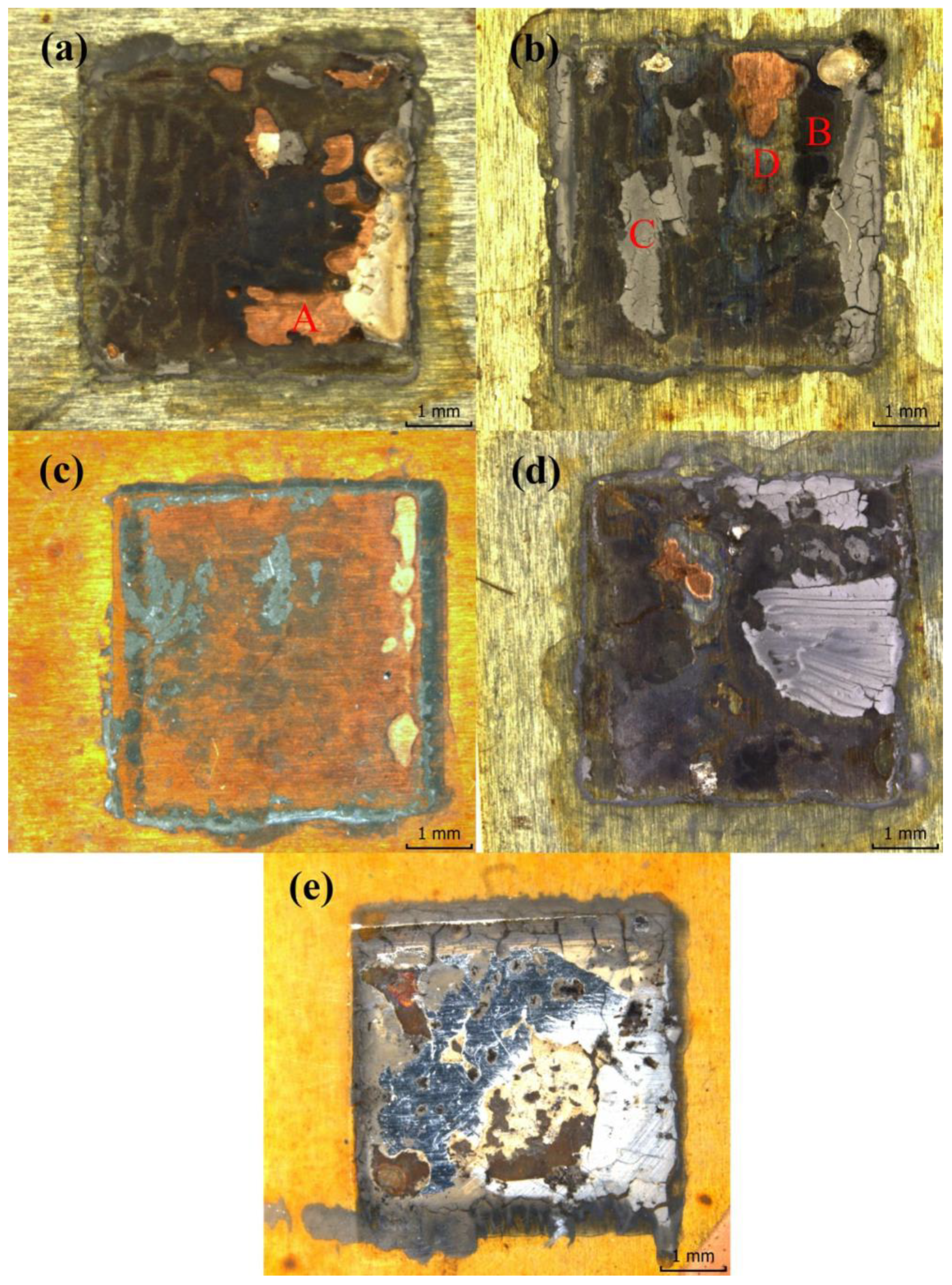
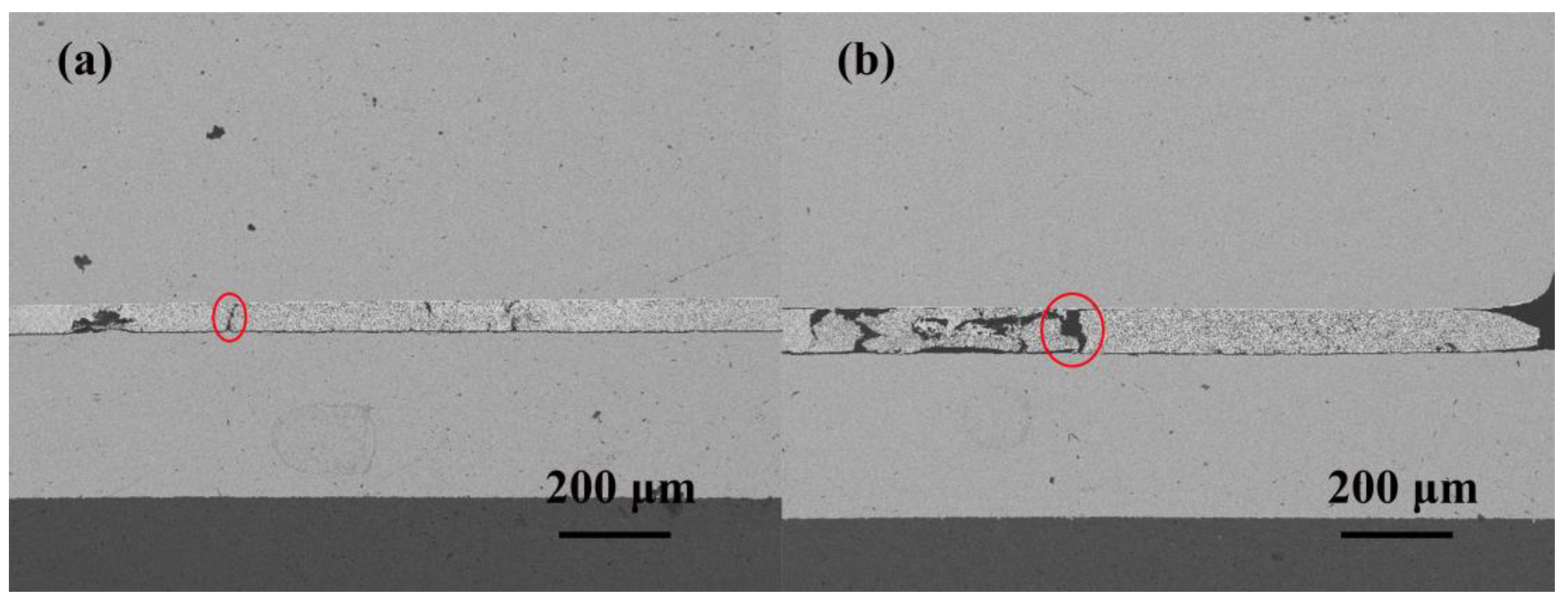
3.1. Effect of the Reliability Test on the Micromorphology
3.2. Effect of the Reliability Tests on the Shear Strength
3.3. EDX Elemental Analysis
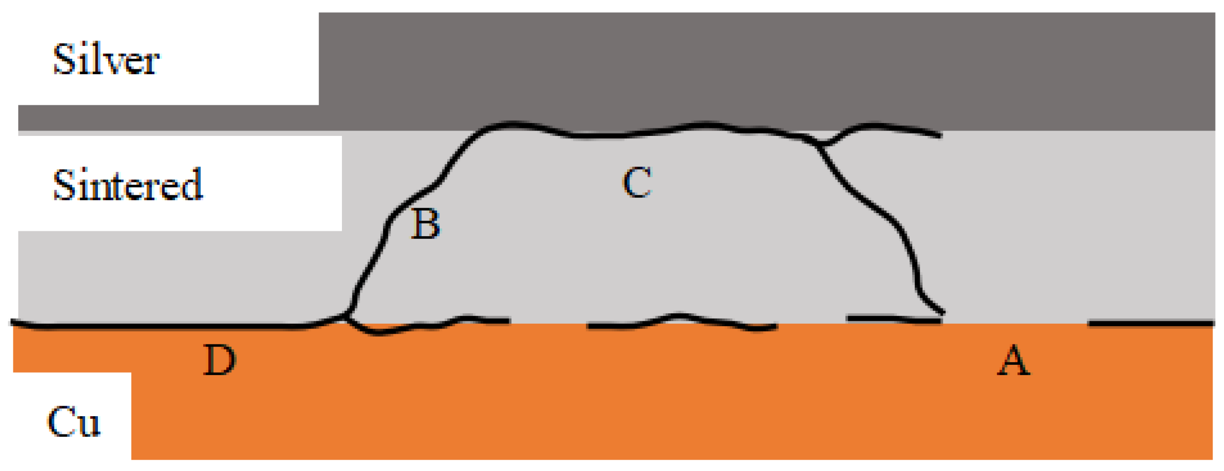
3.4. Analysis of the Fracture Surface Results
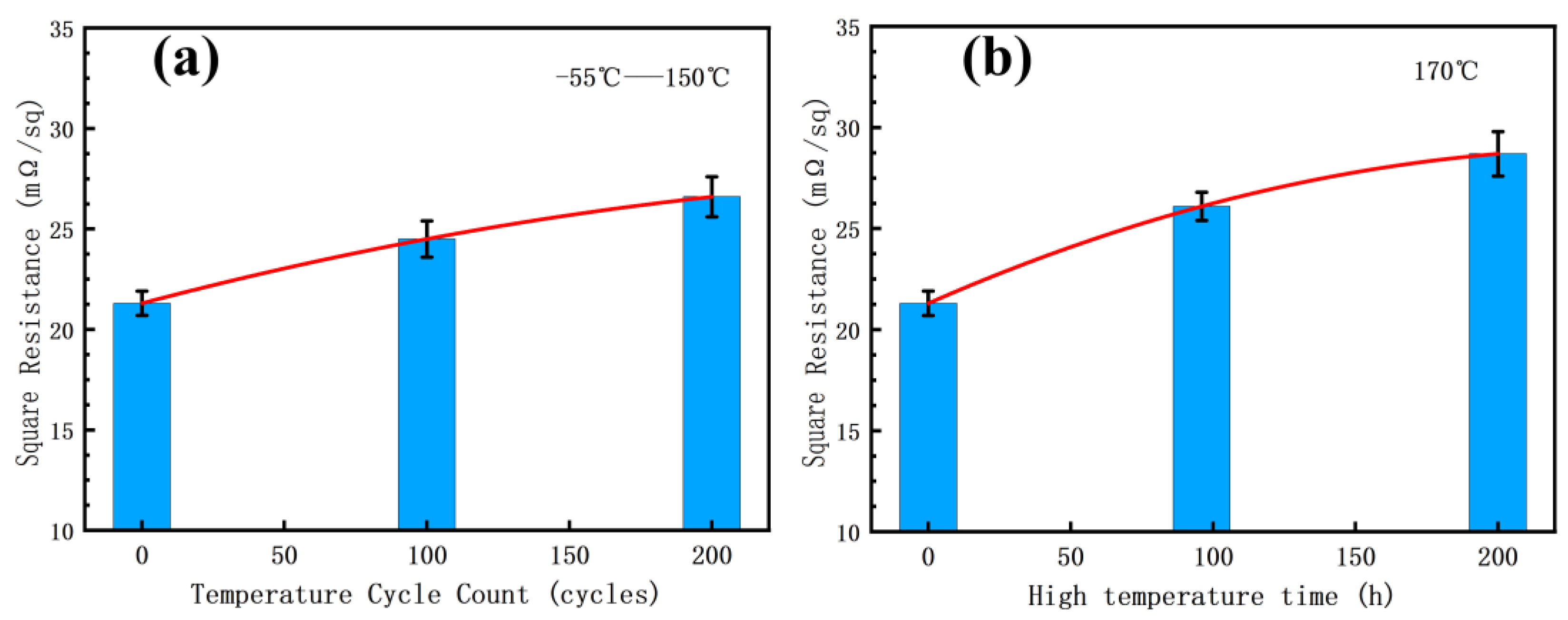
3.5. Effect of Reliability Test on Nano-Silver Square Resistance
4. Conclusions
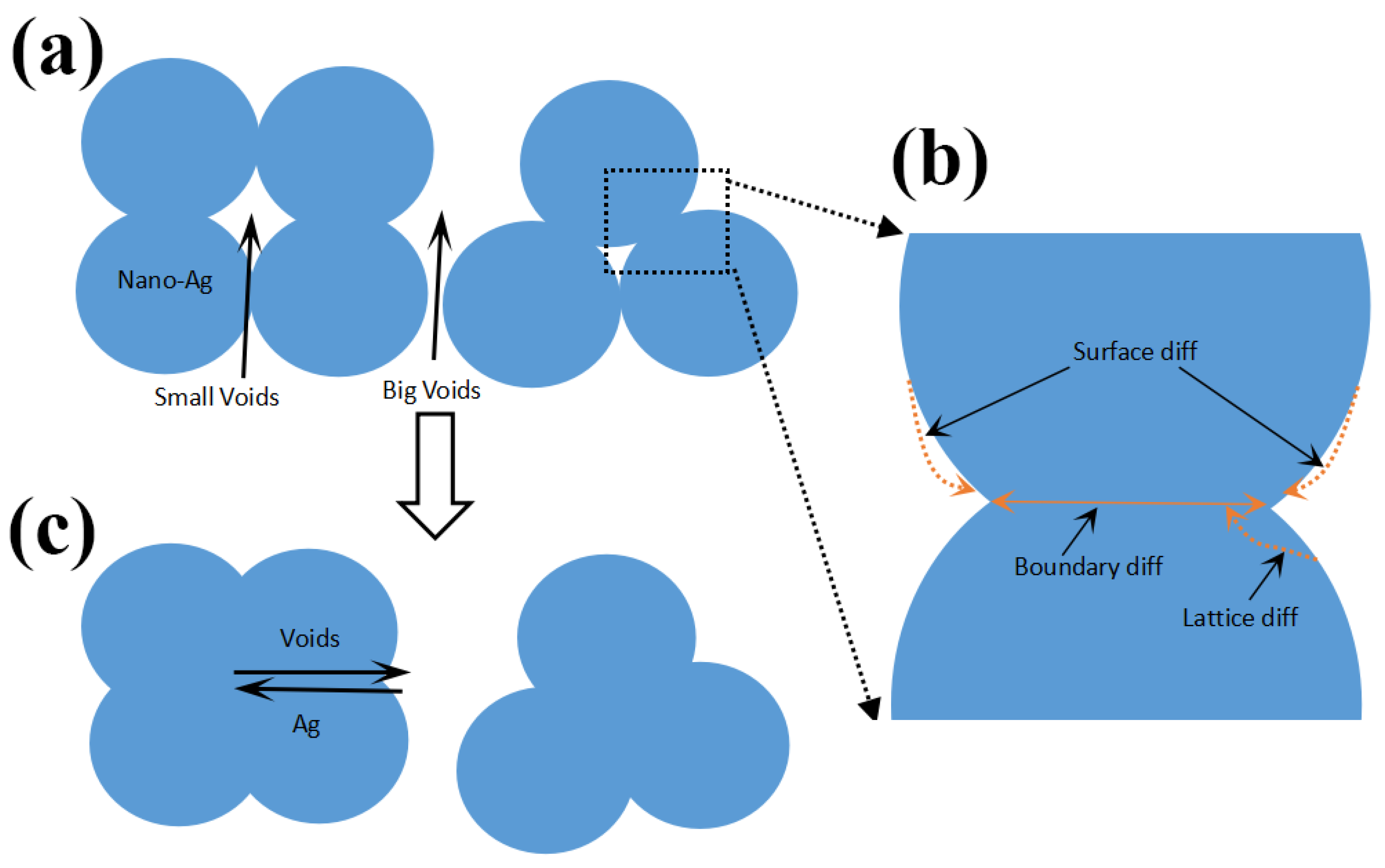
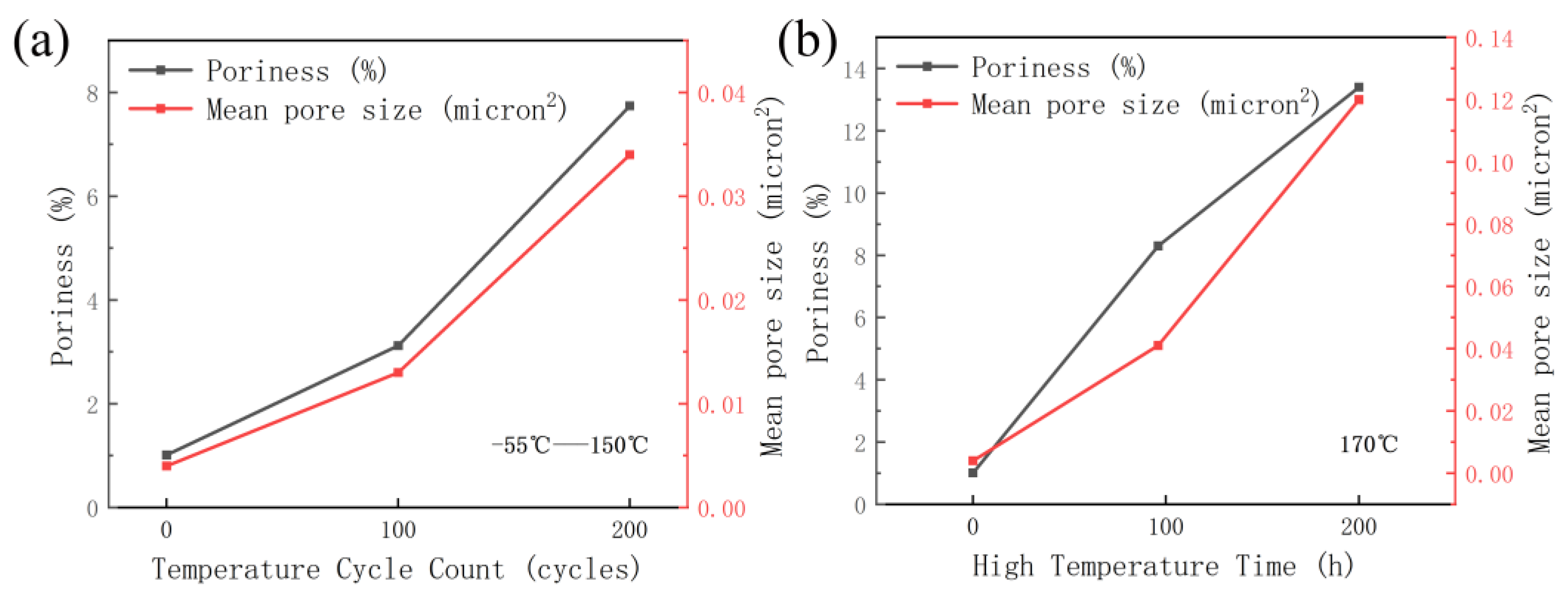
- After high-temperature storage and thermal cycling experiments, the porosity of sintered silver continuously increases, and there is a significant positive correlation between the time in the high-temperature storage and the porosity, with a coefficient of 0.9913. The influence of the high-temperature storage environment on the porosity of visible pores is greater than that of the temperature cycling environment under the same experimental time.
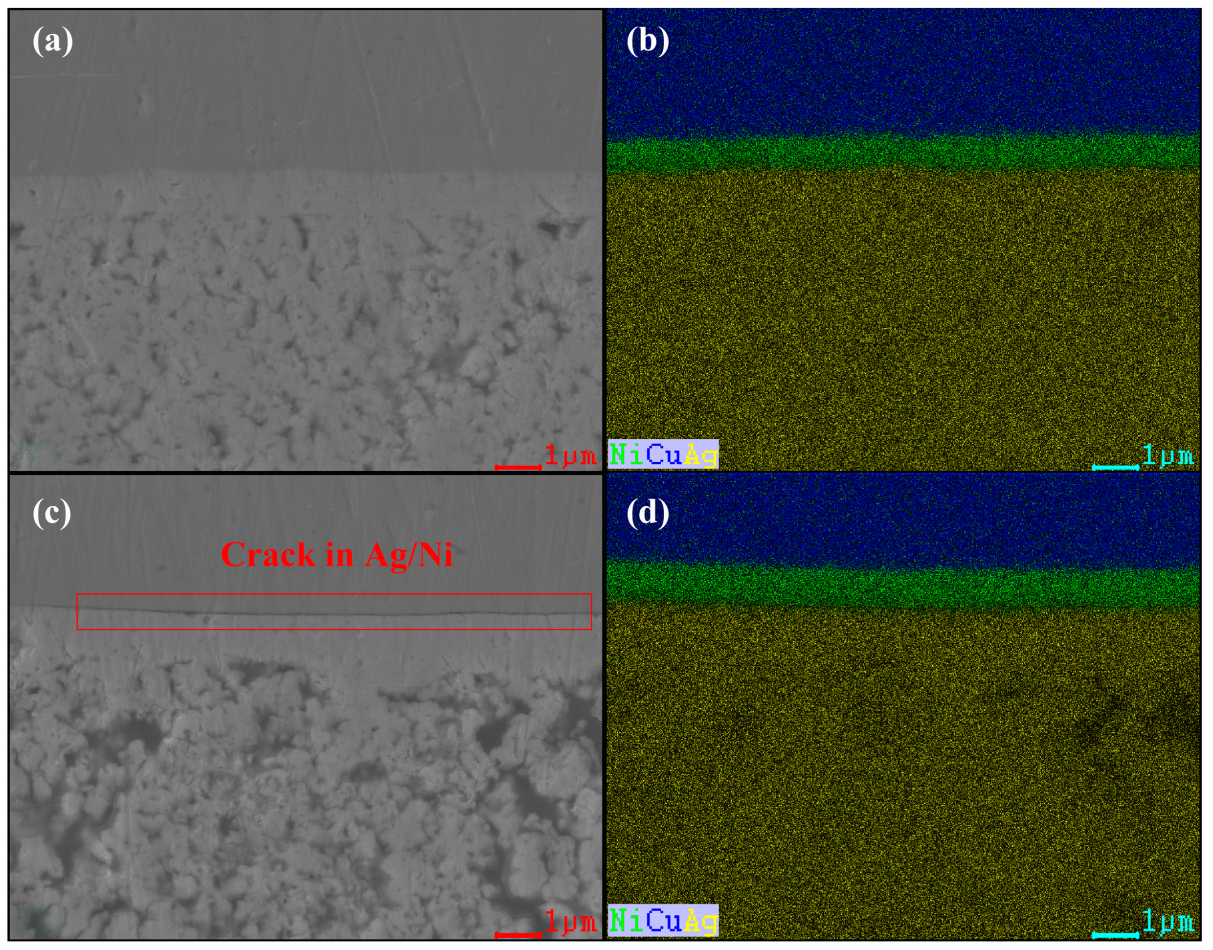
- The bonding effect with the nano-silver layer can be enhanced, and the thermal reliability can be improved by depositing Ni/Ag on the surface of Cu, making it less prone to cracking. However, after 200 h of high-temperature storage, signs of separation between the Ni layer and Ag layer may occur.
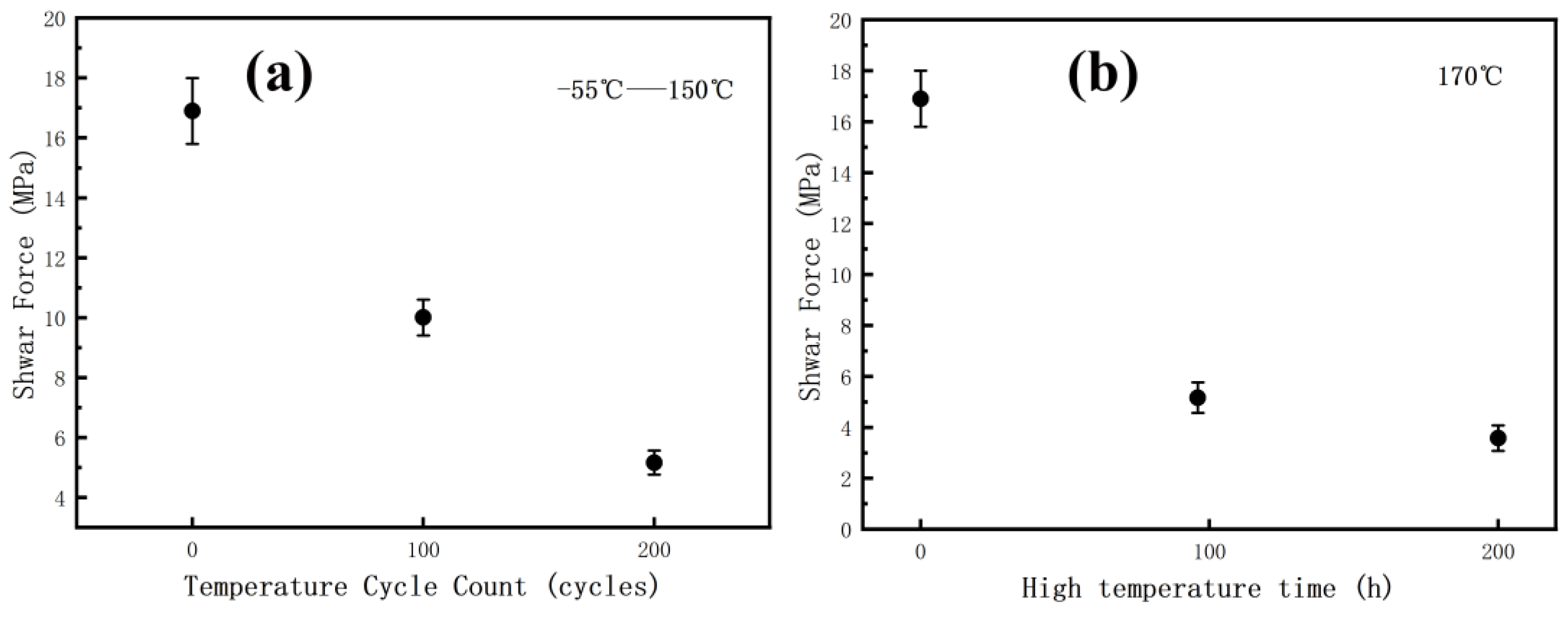
- After the reliability test, the shear force will experience varying degrees of decrease. This decrease can be primarily attributed to the cracking of Cu oxidation at the nano-Ag/Cu interface. The fracture surface exhibits four distinct regional forms, and the shear force shows a strong correlation with the area of close connection between the sintered silver and copper substrate, with a correlation coefficient of 0.994.
- The electrical performances of sintered silver interconnects can be significantly impacted by reliability testing. After 200 h of high-temperature storage, an increase of 35% in the sheet resistance is observed. There is a significant positive correlation between the square resistance and the porosity of the visible pores, with a correlation coefficient of 0.9565.
- The influence of the high-temperature storage environment on the reliability of sintered silver is greater than that of the temperature cycling environment under the same experimental time.
Author Contributions
Funding
Data Availability Statement
Conflicts of Interest
References
- Bindra, A. Innovative Packages Maximize MOSFETs’ Thermal Performance. Electron. Des. 1999, 47, 52–64. [Google Scholar]
- Tummala, R. Next Generation of Packaging beyond BGA, MCM and Flipchip. In Proceedings of the IMC, Plovdiv, Bulgaria, 31 July–5 August 1996. [Google Scholar]
- Wan, J. Research on Filling Flow in Flip Chip Packages; Science Press: Beijing, China, 2008. [Google Scholar]
- Wayne, R.; Johnson, J.E.L. The changing automotive environment: High-temperature electronics. IEEE Trans. Electron. Packag. Manuf. 2004, 27, 164–176. [Google Scholar]
- Yeh, L. Review of heat transfer technologies in electronic equipment. J. Electron. Packag. 1995, 117, 333–339. [Google Scholar] [CrossRef]
- Jiang, C.; Fan, J.; Qian, C.; Zhang, H.; Fan, X.; Guo, W.; Zhang, G. Effects of voids on mechanical and thermal properties of the die attach solder layer used in high-power LED chip-scale packages. IEEE Trans. Compon. Packag. Manuf. Technol. 2018, 8, 1254–1262. [Google Scholar] [CrossRef]
- Feng, H.; Huang, J.; Chen, S.; Zhao, X. The new generation of power chip high temperature resistant packaging connection of domestic and foreign development review. Weld. J. 2016, 37, 120–129. [Google Scholar]
- Kim, H.K.; Liou, H.K.; Tu, K.N. Three-dimensional morphology of a very rough interface formed in the soldering reaction between eutectic SnPb and Cu. Appl. Phys. Lett. 1995, 66, 2337–2339. [Google Scholar] [CrossRef]
- Gomatam, R.R.; Sancaktar, E. Fatigue and failure behavior of silver-filled electronically conductive adhesive joints subjected to elevated temperatures. Adhes. Sci. Technol. 2004, 18, 849–881. [Google Scholar] [CrossRef]
- Zeng, K.; Tu, K.N. Six cases of reliability study of Pb-free solder joints in electronic packaging technology. Mater. Sci. Eng. 2002, 38, 55–105. [Google Scholar] [CrossRef]
- Wang, S.; Li, M.; Ji, H.; Wang, C. Rapid pressureless low-temperature sintering of Ag nanoparticles for high-power density electronic packaging. Scr. Mater. 2013, 69, 789–792. [Google Scholar] [CrossRef]
- Siow, K.S. Mechanical properties of nano-silver joints as die attach materials. J. Alloys Compd. 2012, 514, 6–19. [Google Scholar] [CrossRef]
- Goldmann, L. Self-alignment capability of controlled collapse chip joining. In Proceedings of the 22nd Electronic Component Conference, Orlando, FL, USA, 1 January 1972; pp. 332–335. [Google Scholar]
- Ren, H.; Zhang, H.Q.; Wang, W.G.; Jia, Q.; Peng, P.; Zou, G.S. Research progress of Low-temperature sintering of nano-metal particle solder paste and its joint reliability. Chin. J. Lasers 2021, 48, 126–140. [Google Scholar]
- Zhao, K.; Zhao, J.; Dai, B.; Zhang, X.; Guo, H.; Sun, H.; Zhu, J. Low temperature sintered silver connecting technology of thermal conductive diamond with large size chip. Res. Prog. Solid State Electron. 2021, 41, 65–68. [Google Scholar]
- Zhao, L.; Jing, X.; Li, F.; Li, H.; Li, Y. Research on Reliability of Solder Joints of Nano-Silver Paste. In Proceedings of the Science and Technology Committee of China Academy of Aerospace Electronics Technology, Beijing, China, 15 December 2020; pp. 641–645. [Google Scholar]
- Chou, T.-C.; Huang, S.-Y.; Chen, P.-J.; Hu, H.-W.; Liu, D.; Chang, C.-W.; Ni, T.-H.; Chen, C.-J.; Lin, Y.-M.; Chang, T.-C. Electrical and reliability investigation of Cu-to-Cu bonding with silver passivation layer in 3-D integration. IEEE Transactions on Components. Packag. Manuf. Technol. 2020, 11, 36–42. [Google Scholar] [CrossRef]
- Yang, F. Study on Interconnect Behavior and Reliability of Low Temperature Sintered Nano Silver Solder Joints. Ph.D. Thesis, Harbin Institute of Technology, Harbin, China, 2021. [Google Scholar]
- Zabihzadeh, S.; Van Petegem, S.; Duarte, L.I.; Mokso, R.; Cervellino, A.; Van Swygenhoven, H. Deformation behavior of sintered nanocrystalline silver layers. Acta Mater. 2015, 97, 116–123. [Google Scholar] [CrossRef]
- Yan, H.; Liang, P.; Mei, Y.; Feng, Z. Progress and thinking of non-pressure low temperature sintered nano silver packaging Power electronic devices. Chin. J. Power Sources 2020, 18, 15–23. [Google Scholar]
- Yuan, L. Study on Microstructure and Property of Nano-Silver Paste Joint of Power IGBT and DBC by Low-Temperature Sintering; Tianjin University China: Tianjin, China, 2015. [Google Scholar]
- Paknejad, S.A.; Mannan, S.H. Review of silver nanoparticle based die attach materials for high power/temperature applications. Microelectron. Reliab. 2017, 70, 1–11. [Google Scholar] [CrossRef]
- Morisada, Y.; Nagaoka, T.; Fukusumi, M.; Kashiwagi, Y.; Yamamoto, M.; Nakamoto, M. A low-temperature bonding process using mixed Cu–Ag nanoparticles. J. Electron. Mater. 2010, 39, 1283–1288. [Google Scholar] [CrossRef]
- Hsiao, C.-H.; Kung, W.-T.; Song, J.-M.; Chang, J.-Y.; Chang, T.-C. Development of Cu-Ag pastes for high temperature sustainable bonding. Mater. Sci. Eng. A 2017, 684, 500–509. [Google Scholar] [CrossRef]
- Tan, Y.; Li, X.; Chen, G.; Gao, Q.; Lu, G.-Q.; Chen, X. Effects of thermal aging on long-term reliability and failure modes of nano-silver sintered lap-shear joint. Int. J. Adhes. Adhes. 2020, 97, 102488. [Google Scholar] [CrossRef]
- Wenzhi, Y.; Xiaoyun, Z.; Shuai, P. Effect of Sintering Temperature Rise Rate on Microstructure and Properties of thick copper Film. Heat Treat. Met. 2017, 42, 43–48. [Google Scholar]
- Chen, C.; Suganuma, K.; Iwashige, T.; Sugiura, K.; Tsuruta, K. High-temperature reliability of sintered microporous Ag on electroplated Ag, Au, and sputtered Ag metallization substrates. J. Mater. Sci. Mater. Electron. 2018, 29, 1785–1797. [Google Scholar] [CrossRef]
- Yu, F.; Cui, J.; Zhou, Z.; Fang, K.; Johnson, R.W.; Hamilton, M.C. Reliability of Ag sintering for power semiconductor die attach in high-temperature applications. IEEE Trans. Power Electron. 2016, 32, 7083–7095. [Google Scholar] [CrossRef]
- Pešina, Z.; Vykoukal, V.; Palcut, M.; Sopoušek, J. Shear strength of copper joints prepared by low temperature sintering of silver nanoparticles. Electron. Mater. Lett. 2014, 10, 293–298. [Google Scholar] [CrossRef]
- Tanović, N.; Tanović, L.; Fine, J. Some experimental facts about temperature-induced surface diffusion of Ag during Auger sputter depth profiling of multilayered Ni/Ag thin films. Vacuum 1992, 43, 1177–1180. [Google Scholar] [CrossRef]
- Zhang, X.; Zhu, Y.; Wang, H. Study on effect of sintering temperature on thick film resistance. Electron. Devices 2012, 35, 394–398. [Google Scholar]
- Gan, W.; Yue, Y.; Luo, L.; Pan, Q.; Xiong, Z. Study on preparation and sintering process of lead-free conductive silver paste. Coat. Ind. 2019, 44, 31–36. [Google Scholar]


| Number | Grouping | Conditions | Strength |
|---|---|---|---|
| 1 | Blank group | ||
| 2 | TCT | −55–150 °C | 100 Circle |
| 3 | TCT | −55–150 °C | 200 Circle |
| 4 | HTSL | 170 °C | 96 h |
| 5 | HTSL | 170 °C | 200 h |
| Sample Number | Average Porosity % | Average Pore Size μm2 | Mean Number of Pores/400 μm2 |
|---|---|---|---|
| 1 | 1.01 | 0.004 | 1104 |
| 2 | 3.12 | 0.013 | 998 |
| 3 | 7.74 | 0.034 | 919 |
| 4 | 8.30 | 0.041 | 815 |
| 5 | 13.4 | 0.072 | 749 |
| Group Number | 1 | 2 | 3 | 4 | 5 |
|---|---|---|---|---|---|
| Area A area% | 8.58 | 4.38 | 2.48 | 2.33 | 1.85 |
| Area B area% | 35 | 26 | 13 | 26 | 29 |
| Area C area% | 15 | 22 | 23 | 20 | 41 |
| Area D area% | 41 | 47 | 62 | 30 | 25 |
| Group Number | 1 | 2 | 3 | 4 | 5 |
|---|---|---|---|---|---|
| Square Resistance (mΩ/sq) | 21.3 | 24.6 | 26.8 | 26.1 | 28.7 |
Disclaimer/Publisher’s Note: The statements, opinions and data contained in all publications are solely those of the individual author(s) and contributor(s) and not of MDPI and/or the editor(s). MDPI and/or the editor(s) disclaim responsibility for any injury to people or property resulting from any ideas, methods, instructions or products referred to in the content. |
© 2023 by the authors. Licensee MDPI, Basel, Switzerland. This article is an open access article distributed under the terms and conditions of the Creative Commons Attribution (CC BY) license (https://creativecommons.org/licenses/by/4.0/).
Share and Cite
Tian, Y.; Jian, X.; Zhao, M.; Liu, J.; Dai, X.; Zhou, B.; Yang, X. Effect of Thermal Aging on the Reliability of Interconnected Nano-Silver Solder Joints. Crystals 2023, 13, 1630. https://doi.org/10.3390/cryst13121630
Tian Y, Jian X, Zhao M, Liu J, Dai X, Zhou B, Yang X. Effect of Thermal Aging on the Reliability of Interconnected Nano-Silver Solder Joints. Crystals. 2023; 13(12):1630. https://doi.org/10.3390/cryst13121630
Chicago/Turabian StyleTian, Yangning, Xiaodong Jian, Mingrui Zhao, Jiahao Liu, Xuanjun Dai, Bin Zhou, and Xiaofeng Yang. 2023. "Effect of Thermal Aging on the Reliability of Interconnected Nano-Silver Solder Joints" Crystals 13, no. 12: 1630. https://doi.org/10.3390/cryst13121630