Article

Study of the Bonding Characteristics at β-Ga2O3(201)/4H-SiC(0001) Interfaces from First Principles and Experiment

1
Department of Electronic Engineering, Xi’an University of Technology, Xi’an 710048, China
2
Key Laboratory of Wide Bandgap Semiconductor Materials, Ministry of Education, Xidian University, 2 South Taibai Road, Xi’an 710071, China
*
Author to whom correspondence should be addressed.
Crystals 2023, 13(2), 160; https://doi.org/10.3390/cryst13020160
Submission received: 15 December 2022 / Revised: 6 January 2023 / Accepted: 13 January 2023 / Published: 17 January 2023
(This article belongs to the Special Issue Semiconductor Materials and Devices)

Abstract

:
For the first time, β-Ga2O3 were prepared on 4H-SiC (0001) substrates using a low-pressure chemical vapor deposition (LPCVD) technique. The obtained β-Ga2O3/4H-SiC heterostructures display strongly preferential growth orientation along the <201> of β-Ga2O3. Combining the experimental results, interfacial properties, such as the work of adhesion (Wad), electronic properties and bonding characteristics of β-Ga2O3(201)/4H-SiC(0001) heterointerface were systemically studied using first principles. Four different β-Ga2O3(201)/4H-SiC(0001) interface models composed of different atom stacking sequences were established. It was found that the interface consisting of silicon terminated of 4H-SiC (0001), and oxygen terminated of β-Ga2O3(201) (Si-O) has the lowest relaxation energy and the highest stability. Results indicated that the binding of interface Si and C to the O atoms is stronger than that to the Ga atoms. The results of the difference charge density and electron localization function reveals that the Si and C atoms at interface are bonded with O atoms of β-Ga2O3 by covalent bonds, in which Si-O and C-O covalent bonds play a favorable role in the final stable configurations formation. This work will provide a further understanding of the various electronic behaviors of the β-Ga2O3(201)/4H-SiC(0001) heterointerface.

1. Introduction

The monoclinic gallium oxide (β-Ga2O3) has attracted widespread attention in automobile, high-speed rail power system, new energy, semiconductor power devices, communication electronics and other fields because of its band gap of 4.9 eV [1,2,3]. Unfortunately, its interface thermal management is a downside; this can cause significant damage to electronic devices [4,5]. Thus, there have been intense efforts to study the β-Ga2O3/4H-SiC heterointerface, in which the 4H-SiC is used as a high thermal conductivity semiconductor material (4.9 W/cm K) as a thermal conductivity substrate. Worldwide, an enormous amount of research has shown that the interface has a notable influence on the properties of heterogeneous interfaces [6,7]. Thus, the interface formation and the bonding characteristics of the β-Ga2O3(201)/4H-SiC(0001) heterointerface are worth investigating.
To date, methods such as laser molecular beam epitaxy (L-MBE) technique [8], radio frequency sputtering [9], ion-cutting technique [10], gallium evaporation in oxygen plasma [11] and pulsed laser deposition (PLD) [12] are used to prepare β-Ga2O3/SiC heterostructures. The experiment by Neeraj Nepal et al. [13] found that Ga2O3(201) and SiC(0001) formed a clear interface between the two components, and it was believed that this orientation contributed to a better combination between Ga2O3 and SiC. Moreover, many researchers have applied the first principle to study the interface between other semiconductor substrates and Ga2O3. The first-principle calculation method was used by Yu et al. [14] to study the electronic structure and properties of Ga2O3/CuAlO2 heterojunctions. They found that interface with oxygen–copper terminals is more stable than that oxygen–aluminum terminals. He et al. [15] studied six staking sequences at AlN(0001)/Ga2O3(100) interfaces using the first-principCle calculation method which revealed high thermodynamic stability and relatively strong interface bonding for the B-Al, B-N, and C-N models. Unfortunately, it is difficult to use effective experiment characterization to study the interfacial electronic interaction between β-Ga2O3 and 4H-SiC. Hence, there is still an urgent need to investigate the interfacial bonding characteristics of β-Ga2O3(201)/4H-SiC(0001) heterostructure based on first-principles calculation.
In this paper, the atomic structure and bonding characteristics of β-Ga2O3/4H-SiC(0001) have been investigated using first principles and experimental methods. The geometry structures, work of adhesions, stability, bonding characteristics and electronic properties of β-Ga2O3(201)/4H-SiC(0001) were deeply explored. It is important that interfacial adhesion and bonding characteristics are taken into account when studying nucleation on substrates. The results show that the work of adhesion of β-Ga2O3/4H-SiC(0001) at the oxygen–silicon terminal is stronger than that at the oxygen–carbon terminal. Based on the difference charge density and electron localization function, Si-O polar covalent bonds were formed near the Si-O interface, which made the interface more stable. According to the results, LPCVD can synthesize β-Ga2O3 films on 4H-SiC substrates for using in high power electronic devices.

2. Experimental and Calculation Methodology

2.1. Calculation Methodology

Based on DFT [16,17], the β-Ga2O3/4H-SiC with interfaces connecting β-Ga2O3( 2 ¯ 01) to 4H-SiC(0001) has been investigated. The exchange-correlation function is selected GGA-PBE [18]. In order to gain a stable configuration and ensure calculation accuracy, the total energy and k-points grid are tested. The optimized plane-wave cutoff energy and k-point grid are set to 500 eV and 2 × 11 × 1, respectively. The β-Ga2O3/4H-SiC interface model includes six β-Ga2O3 layers and five 4H-SiC carbide diatomic layers, in which the suspended bond is passivated by hydrogen atoms. A vacuum of 15 Å was employed on the two side materials to separate the interaction between periodic slabs. The valence electron is configured: 3d104s24p1 for Ga, 2s22p4 for O, 2s22p2 for C, 3s23p2 for Si and 1s for H. The maximum total energy is set to 10−5 eV and forces on atoms in the range of −0.03 eV/Å.

2.2. Experimental

β-Ga2O3 films were grown on commercially available 4° ± 0.5° off-axis n-type 4H-SiC substrates (10 mm × 10 mm × 0.35 mm) via a double temperature zone LPCVD system (see Figure 1a). High purity gallium metal (≥99.9999%), oxygen (O2, 5N) and Argon (Ar, 5N) were used as the gallium source, oxygen precursors and carrier gas, respectively. Growth pressure was always kept at 100 Pa. Figure 1b shows the diagram of the growth process with time dependent on temperature The evaporation temperature of gallium metal and deposition temperature have been maintained at 950°C and 650°C, respectively. The deposition process of β-Ga2O3 films were shown in Figure 1c. In Figure 1c, high purity oxygen (5N) reacts with gallium vapor to form gallium oxide, which is transported and deposited onto the surface of a 4H-SiC substrate by high purity Ar (5N).

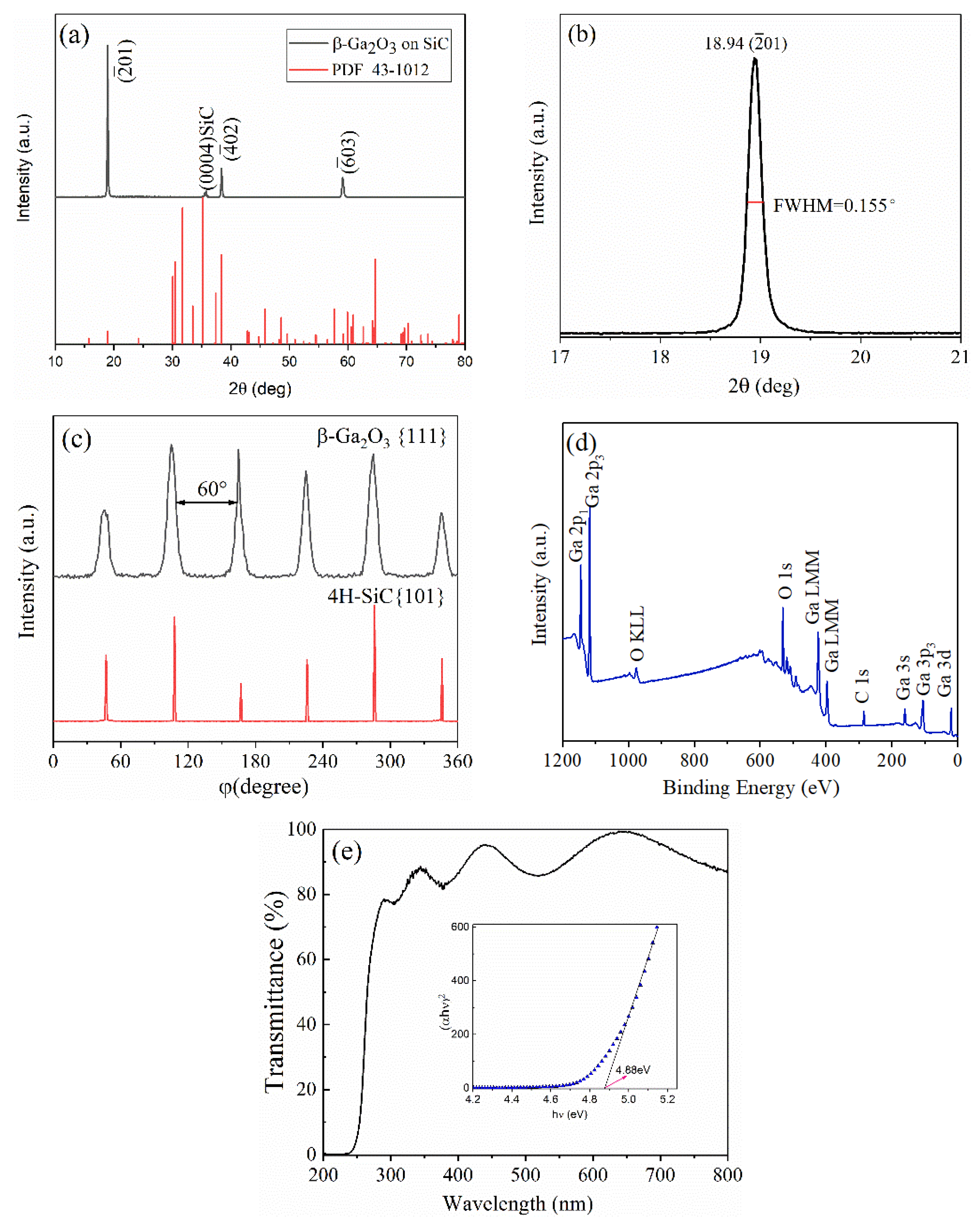
3. Results and Discussion

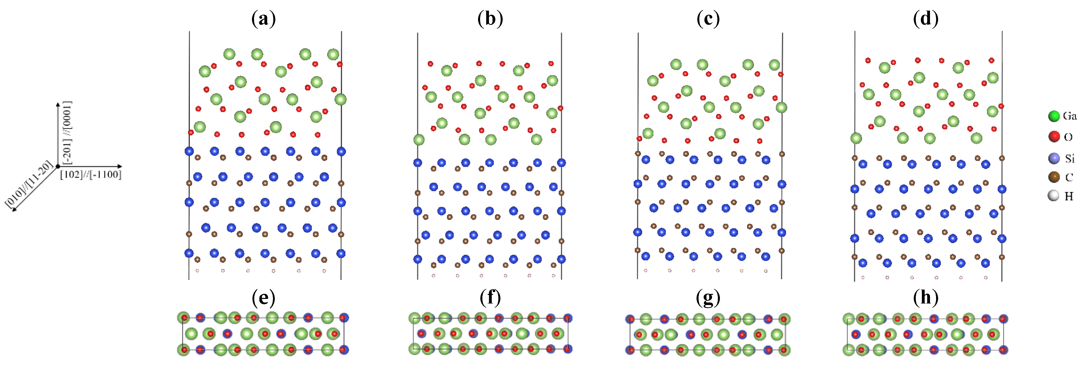
3.1. Computational Medels

The optimized bulk material parameters of monoclinic gallium oxide are a = 12.49 Å, b = 3.10 Å, c = 5.91 Å and 4H-SiC are a = b = 3.09 Å, c/a = 3.28. Our optimized lattice constants show a good agreement with experimental and theoretical results [14,19,20,21,22]. According to the XRD θ~2θ and off-specular phi-scan results, the (1 × 1) β-Ga2O3(201)–(3×√3) 4H-SiC(0001) interface models were established to simulate the interface between β-Ga2O3 and 4H-SiC. The lattice misfit along the b direction is 0.3% with 1bβ-Ga2O3(010) matching to 1b4H-SiC(1120), while along a direction, the mismatch is about 6.9%, with 3a4H-SiC(1100) matching to 1aβ-Ga2O3(102). The different terminated atoms of (0001)4H-SiC and (201)β-Ga2O3 means that there are four kinds of interface models: Si-O terminated, Si-Ga terminated, C-O terminated and C-Ga terminated. The side view and top view of β-Ga2O3(201)/4H-SiC(0001) models are illustrated in Figure 2a–h. The lattice constant of β-Ga2O3(201)/4H-SiC(0001) interface are: a = 15.56 Å, b = 3.09 Å, c = 36.55 Å, α = β = γ = 90°. The interface models adopted a 5-layer slab of 4H-SiC and 6-layer slab of β-Ga2O3(201).

3.2. Work of Adhesion

Interface bonding can be evaluated by work of adhesion (Wad) and be expressed as the work to hive off a complete interface into two free slabs. The Wad [23,24,25] is determined by Equation (1):
W a d = ( E β G a 2 O 3 + E 4 H S i C   E β G a 2 O 3 /   4 H S i C   ) / A i n t e r f a c e
where E β G a 2 O 3 and E 4 H S i C   are the total energy of the isolated β-Ga2O3 layer and 4H-SiC layer, respectively. E β G a 2 O 3 /   4 H S i C devotes total energy of the heterointerface. Ainterface is the interfacial area of β-Ga2O3( 2 ¯ 01)/4H-SiC(0001). A positive value of Wad represents that the reversible work necessary to separate theβ-Ga2O3(201)/4H-SiC(0001) interface into β-Ga2O3 slab and 4H-SiC slab. According to formula (1), Wad of four different interface models are calculated. The calculated Wad, total energy, bond length and interface spacing are shown in Table 1 with different configurations. It shows that the calculated Wad of Si-O, Si-Ga, C-O and C-Ga interface is 8.5, 3.1, 4.3 and 3.4 J/m2, respectively. As shown in Table 1, the optimized interface spacing of Si-O, Si-Ga, C-O and C-Ga interface is 1.7 Å, 2.3 Å, 1.5 Å and 1.9 Å, respectively. Obviously, the Si-O interface presents the lowest relaxation energy and largest Wad among the four different terminals, indicating that the bonding strength at this interface is the strongest. The Si-Ga model and C-Ga model have smaller work of adhesion. Thus, among the four structures, it can be seen that the stability of Si-O interface system is strongest. There may be a difference in the oxidation process between the 4H-SiC surface at the Si-terminated and the 4H-SiC surface at the C-terminated, resulting in a stronger Si-O bond than a C-O bond on the 4H-SiC surface [26]. The larger the Wad, the more difficult the interface is to separate, indicating a more stable interface structure, which means that bonding strength is as follows: Si-O > C-O > C-Ga > Si-Ga.

3.3. Bonding Characteristics

It is well known that high stability and strength can be bound up to the chemical bond type at the interfaces. To understand the electron transfer at the four interfaces, the difference charge density of the β-Ga2O3/4H-SiC heterointerfaces were calculated (see Figure 3). The difference charge density along the z direction Δρ (z) [27,28] is as follows:
Δ ρ ( z ) = Δ ρ ( z ) β G a 2 O 3 /   4 H S i C   Δ ρ ( z ) β G a 2 O 3   Δ ρ ( z ) 4 H S i C  
where Δ ρ ( z ) β G a 2 O 3 /   4 H S i C is the total charge density of the β-Ga2O3/4H-SiC interface, Δ ρ ( z ) β G a 2 O 3 and Δ ρ ( z ) 4 H S i C   are the charge density of individual β-Ga2O3(201) slab and 4H-SiC(0001) slab, respectively. The four figures show that there is a significant charge transfer at the interface atoms. The yellow and blue sections present the aggregation and depletion of charges, respectively. The distinct charge accumulation between Si and O is closer to O, suggesting a polar covalent bond in Figure 3a. There is the charge accumulated between Si and Ga atoms, implying a covalent bond in Figure 3b. Figure 3c shows the electrons of O atoms on β-Ga2O3 and the electrons of C atoms on 4H-SiC side are transferred to the middle of C and O atoms at the interface. The electrons are accumulated at C atoms and Ga atoms at interface in Figure 3d. It is shown that Si and C prefer to combine with O atom rather than Ga atom of β-Ga2O3(201). Above all charge transfer mainly occurs between several atomic layers at the heterointerface.
To further calculate the net charge transfer of interfacial atoms on β-Ga2O3/4H-SiC interfaces, we analyzed the Bader charge. The Bader charge of Si-O interface, Si-Ga interface, C-O interface and C-Ga interface are 4.63 e, 0.157 e, 2.86 e and −1.61 e, respectively. For Si-O interface, 4.63 e is transferred from 4H-SiC to β-Ga2O3, each O atom at the interface receive about 0.77 e from Si atoms. While only 0.157 e is also transferred from 4H-SiC to β-Ga2O3 at the Si-Ga interface, suggesting gallium atoms and silicon atoms almost share electrons. For the C-O model, there are 2.86 e transferred from 4H-SiC to β-Ga2O3. The 3.11 e is transferred from Si atoms to interfacial C atoms and then 2.86 e is further transferred from interfacial C atoms to O atoms of β-Ga2O3. For C-Ga interface, the 1.61 e transferred from Ga atoms to interfacial C atoms. In conclusion, the charge tends to transfer to atoms with greater electronegativity. These results explain that, compared with the other three interface models, the Si-O interface models transferred the most electrons, and is the most stable.
Figure 4 shows the electron localization function of β-Ga2O3(201)/4H-SiC(0001). High-localized electrons are represented by red, and high-delocalized electrons are represented by blue. It is assumed that charge transfer takes place between only the nearest atomic layers [29]. Obviously, in all heterojunction systems, the bonds between atoms are covalent bonds. For the Si-O interface, O atoms have a strong charge accumulation and there is a low localization degree around Si atoms, resulting in a strong Si-O polar covalent bond with bond length 1.66 Å. In Figure 4b, there is a high localization degree in the middle of Si atoms and Ga atoms, indicating Si-Ga covalent bond and an average bond length of 2.44 Å, which is highly consistent with the result of the Bader charge. From Figure 4c, the high local state between C and O indicates that there is a C-O polar covalent bond at β-Ga2O3(201)/4H-SiC(0001) interface, with the bond length 1.47 Å. Obviously, according to the localization degree between the C and Ga atom, the interaction for C-Ga seems relatively weak in Figure 4d, which is weak a C-Ga covalent bond with an average bond length of 1.95 Å. In Table 1, after optimizing the interfacial models, it is clearly observed that the bond length of Si-O terminated and C-O terminated is reduced, resulting in a more stable structure. The results show that the bonding mechanism of β-Ga2O3(201)/4H-SiC(0001) is a covalent bond, and the bonding strength between silicon atoms and oxygen atoms is the stronger than other interfacial models. Si-O and C-O polar covalent bonds play a favorable role in the formation of stable configurations.
Based on the above growth conditions, we prepared single crystal β-Ga2O3 thin films on (0004) SiC substrate using the LPCVD technique. Figure 5a shows the XRD pattern of β-Ga2O3/4H-SiC. The diffraction peak near 35.58° corresponded to (0004) SiC substrate. The other three different peaks observed at 18.94°, 38.40° and 59.10° are from the (201), ( 4 ¯ 02) and ( 6 ¯ 03), respectively. The sample was indexed according to JCPDS No. 43-1012 [30]. The XRD result indicates that the as-prepared β-Ga2O3 films via LPCVD on 4H-SiC substrate exhibited preferentially selective orientation along <201>. The FWHM is the full width at half of the peak maximum. The full width at half maximum (FWHM) was calculated to be 0.155° by fitting with Gaussian functions of the lower angle diffraction peak of (201) in Figure 5b. The average grain size (D) of β-Ga2O3 films is calculated by the following expressions [31]:
D = k λ F W H M cos θ
where θ is the Bragg’s angle, λ corresponds to the X-ray wavelength (λ = 0.15406 nm) and k = 0.89. The calculated average grain size D is 51.4 nm. Crystallinity is increased and crystal quality is improved with a smaller FWHM. Figure 5c shows the off-specular phi-scan of β-Ga2O3(111) and 4H-SiC(101) planes. For β-Ga2O3(111) plane, the Bragg angle θ and rotation angle χ are 17.59° and 80.53°, respectively. It is well known that the (111) plane of β-Ga2O3 single crystal has twofold symmetry along the normal direction of <010>. As shown in Figure 5c, there are six diffraction peaks separated by 60° of β-Ga2O3, indicating that a tripartite domain structure exists inside the β-Ga2O3 film [32,33]. The Bragg angle θ and rotation angle χ of 4H-SiC are17.39° and 75.14°, respectively. Due to the 4H-SiC is six-fold symmetry along [0001] direction, there is a diffraction peak every 60° in the diffraction pattern. In comparing the off-specular phi-scan of β-Ga2O3(111) to 4H-SiC (101) planes, it is found that the six φ angles are identical in Figure 5c. Therefore, the 4H-SiC (0001) plane is parallel to (201) plane of the monoclinic gallium oxide (β-Ga2O3(201)||4H-SiC(0001)). Thus, high-quality (201) β-Ga2O 3 film was successfully deposited on the (0001) 4H-SiC substrate. The chemical composition states of β-Ga2O3 thin films were studied by XPS measurement. Figure 5d displays a survey scan of the as-deposited β-Ga2O3 thin films, including photoelectron lines Ga 2p, Ga 3s, Ga 3d, Ga 3p, O 1s and C 1s, respectively [34]. No peak of Si belonging to 4H-SiC substrate was observed as the epitaxial Ga2O3 was thick enough. It is worth noting that the element energy shifts of the C, O and Ga peaks were calibrated by C1s peak at 284.8 eV, which was considered to have originated from the absorption of hydrocarbons or CO2 on the surface. Figure 5e shows the optical transmittance spectrum of the β-Ga2O3/4H-SiC heterojunction in the test coverage of 200 to 800 nm. It is possible to calculate the optical band gap of materials by measuring their transmittance. The smaller band gap of 4H-SiC than β-Ga2O3 means that light sources less than 300 nm cannot pass through the substrate and are all absorbed. Thus, we grow gallium oxide thin films on quartz to measure their optical band gap. Transmittance of β-Ga2O3 film is more than 90% and has weak absorption for wavelengths over 300 nm. In addition, the β-Ga2O3 thin films have high absorptivity in the deep ultraviolet region (200–300 nm) with an absorption edge located at around 270 nm. As can be seen in the inset of Figure 5e, the optical band gap (4.88 eV) is estimated by using the Tauc plot [35], which almost consistent with the values of 4.86 eV [14].

4. Conclusions

In summary, the electronic properties and bonding strength of four different models of β-Ga2O3(201)/4H-SiC(0001) have been deeply studied by calculations and experimental investigations in this work. The crystalline structures, chemical compositions, optical properties and interface bonding characteristics of the as-prepared heterostructures were all comprehensively investigated using experiment and first principles. β-Ga2O3 films are pure phase with highly preferential growth orientation along the <201> and show high transmittance at wavelengths over 280 nm. The XRD phi-scan reveals that epitaxial relationship of β-Ga2O3 and 4H-SiC is β-Ga2O3(201)||4H-SiC(0001). The results show that the Wad of β-Ga2O3(201) with an oxygen–silicon terminal of 4H-SiC(0001) is stronger than that of the other three models, in which it can be seen that the stability of Si-O interface system is strongest. The electron localization function analysis shows that the dominant interfacial chemical bonds are the Si–O polar covalent bond and C–O covalent bond for the Si-termination and C-termination of β-Ga2O3(201)/4H-SiC(0001) interface, respectively. The results show that the Si-O and C-O covalent bonds play a dominant role in the formation of stable configurations. The results obtained in this work also illustrate that LPCVD is a suitable method to synthesize β-Ga2O3 films on 4H-SiC substrates for high power electronic devices.

Author Contributions

Conceptualization, J.H. and X.H.; methodology, J.H. and B.X.; software, B.X.; formal analysis, X.W. and J.M.; investigation, B.X.; resources, J.M.; data curation, X.W.; writing—original draft preparation, B.X.; writing—review and editing, J.H. and B.X.; supervision, H.P.; project administration, J.H.; funding acquisition, J.H. All authors have read and agreed to the published version of the manuscript.

Funding

This research received no external funding.

Institutional Review Board Statement

Not applicable.

Informed Consent Statement

Informed consent was obtained from all subjects involved in the study.

Data Availability Statement

Not applicable.

Acknowledgments

This work was supported by the National Natural Science Foundation of China (Grant No. 61904146 and No. 62104190); Shaanxi innovation capability support project (2021TD-25).

Conflicts of Interest

The authors declare no conflict of interest.

References

  1. Wu, C.; Wu, F.M.; Ma, C.Q.; Li, S.; Liu, A.P.; Yang, X.; Chen, Y.C.; Wang, J.B.; Guo, D.Y. A general strategy to ultrasensitive Ga2O3 based self-powered solar-blind photodetectors. Mater. Today Phys. 2022, 23, 100643. [Google Scholar] [CrossRef]
  2. Wu, C.; Guo, D.Y.; Zhang, L.Y.; Li, P.G.; Zhang, F.B.; Tan, C.K.; Wang, S.L.; Liu, A.P.; Wu, F.M.; Tang, W.H. Systematic investigation of the growth kinetics of β-Ga2O3 epilayer by plasma enhanced chemical vapor deposition. Appl. Phys. Lett. 2020, 116, 072102. [Google Scholar] [CrossRef]
  3. Cao, J.; Chen, L.; Chen, X.; Zhu, Y.; Dong, J.; Wang, B.; He, M.; Wang, X. Performance Improvement of Amorphous Ga2O3 /P-Si Deep Ultraviolet Photodetector by Oxygen Plasma Treatment. Crystals 2021, 11, 1248. [Google Scholar] [CrossRef]
  4. Yu, Y.T.; Xiang, X.Q.; Zhou, X.Z.; Zhou, K.; Xu, G.W.; Zhao, X.L.; Long, S.B. Device topological thermal management of β-Ga2O3 Schottky barrier diodes. Chin. Phys. B 2021, 30, 067302. [Google Scholar] [CrossRef]
  5. Yuan, C.; Zhang, Y.; Montgomery, R.; Kim, S.; Shi, J.; Mauze, A.; Itoh, T.; Speck, J.S.; Graham, S. Modeling and analysis for thermal management in gallium oxide field-effect transistors. J. Appl. Phys. 2020, 127, 154502. [Google Scholar] [CrossRef] [Green Version]
  6. Xiao, J.B.; Yao, J.P. First Principle Calculation of Electronic Structure and Stabilities of TiC/Mg Composites Interfaces. IOP Conf. Ser. Mater. Sci. Eng. 2020, 774, 012096. [Google Scholar] [CrossRef]
  7. Lv, W.; Yan, L.; Pang, X.; Yang, H.; Qiao, L.; Su, Y.; Gao, K. Study of the stability of α-Fe/MnS interfaces from first principles and experiment. Appl. Surf. Sci. 2020, 501, 144017. [Google Scholar] [CrossRef]
  8. Qu, Y.; Wu, Z.; Ai, M.; Guo, D.; An, Y.; Yang, H.; Li, L.; Tang, W. Enhanced Ga2O3/SiC ultraviolet photodetector with graphene top electrodes. J. Alloy. Compd. 2016, 680, 247–251. [Google Scholar] [CrossRef]
  9. Byun, D.W.; Lee, Y.J.; Oh, J.M.; Schweitz, M.A.; Koo, S.M. Morphological and electrical properties of β-Ga2O3 /4H-SiC heterojunction diodes. Electron. Mater. Lett. 2021, 17, 479–484. [Google Scholar] [CrossRef]
  10. Xu, W.; You, T.; Wang, Y.; Shen, Z.; Liu, K.; Zhang, L.; Sun, H.; Qian, R.; An, Z.; Mu, F.; et al. Efficient thermal dissipation in wafer-scale heterogeneous integration of single-crystalline β- Ga2O3 thin film on SiC. Fundam. Res. 2021, 1, 691–696. [Google Scholar] [CrossRef]
  11. Nakagomi, S.; Momo, T.; Takahashi, S.; Kokubun, Y. Deep ultraviolet photodiodes based on β-Ga2O3 /SiC heterojunction. Appl. Phys. Lett. 2013, 103, 072105. [Google Scholar] [CrossRef] [Green Version]
  12. Yu, J.; Nie, Z.; Dong, L.; Yuan, L.; Li, D.; Huang, Y.; Zhang, L.; Zhang, Y.; Jia, R. Influence of annealing temperature on structure and photoelectrical performance of β-Ga2O3 /4H-SiC heterojunction photodetectors. J. Alloy. Compd. 2019, 798, 458–466. [Google Scholar] [CrossRef]
  13. Nepal, N.; Katzer, D.S.; Downey, B.P.; Wheeler, V.D.; Nyakiti, L.O.; Storm, D.F.; Hardy, M.T.; Freitas, J.A.; Jin, E.N.; Vaca, D.; et al. Heteroepitaxial growth of β-Ga2O3 films on SiC via molecular beam epitaxy. J. Vac. Sci. Technol. A Vac. Surf. Film. 2020, 38, 063406. [Google Scholar] [CrossRef]
  14. Yu, M.; Wang, H.; Wei, W.; Peng, B.; Yuan, L.; Hu, J.; Zhang, Y.; Jia, R. Analysis of electronic structure and properties of Ga2O3 /CuAlO2 heterojunction. Appl. Surf. Sci. 2021, 568, 150826. [Google Scholar] [CrossRef]
  15. He, X.; Hu, J.; Zhang, Z.; Liu, W.; Song, K.; Meng, J. Study on the interface electronic properties of AlN(0001)/ β- Ga2O3100). Surf. Interfaces 2022, 28, 101585. [Google Scholar] [CrossRef]
  16. Xu, P.; Gui, X.; Zhang, X.; Zhang, M.; Liu, G.; Guo, Q.; Qiao, G. Wetting and interfacial behavior of Al–Ti/4H–SiC system: A combined study of experiment and DFT simulation. Ceram. Int. 2021, 47, 32545–32553. [Google Scholar] [CrossRef]
  17. Wang, L.; Dhar, S.; Feldman, L.C.; Kuroda, M.A. Nitrogen-Induced Changes in the Electronic and Structural Properties of 4H-SiC (0001)/SiO2 Interfaces. Phys. Status Solidi (B) 2022, 259, 2100224. [Google Scholar] [CrossRef]
  18. Liu, B.B.; Yang, J.F. Mg on adhesion of Al (111)/3C-SiC (111) interfaces from first principles study. J. Alloy. Compd. 2019, 791, 530–539. [Google Scholar] [CrossRef]
  19. Zacherle, T.; Schmidt, P.C.; Martin, M. Ab initio calculations on the defect structure of beta- Ga2O3. Phys, Rev. B 2013, 87, 23520. [Google Scholar]
  20. Geller, S. Crystal Structure of β-Ga2O3. J. Chem. Phys. 1960, 33, 676–684. [Google Scholar] [CrossRef]
  21. Su, J.; Guo, R.; Lin, Z.; Zhang, S.; Zhang, J.; Chang, J.; Hao, Y. Unusual electronic and optical properties of two-dimensional Ga2O3 predicted by density functional theory, J. Phys. Chem. C. 2018, 122, 24592–24599. [Google Scholar] [CrossRef]
  22. Park, C.; Cheong, B.-H.; Lee, K.-H.; Chang, K.J. Structural and electronic properties of cubic, 2 H, 4 H, and 6 H SiC. Phys. Rev. B 1994, 49, 4485–4493. [Google Scholar] [CrossRef] [PubMed]
  23. Wang, Y.; Li, M.; Peng, P.; Gao, H.; Wang, J.; Sun, B. Preferred orientation at the Al/graphene interface: First-principles calculations and experimental observation. J. Alloy. Compd. 2022, 900, 163304. [Google Scholar] [CrossRef]
  24. Wang, Y.; Wang, W.; Fang, S.; Dai, B.; Zhu, J. The interface characteristics of TiN (100)/MgO (100) multilayer on oxidized Si (100) substrate via first-principle calculations and experimental investigation. Mol. Simul. 2021, 47, 552–559. [Google Scholar] [CrossRef]
  25. Liu, X.; Dong, H.; Lv, X.; Bai, C.; Hu, N.; Wen, L.; Yang, Z. The adhesion, stability, and electronic structure of γ-TiAl/VN interface: A first-principle study. Appl. Phys. A 2018, 124, 531. [Google Scholar] [CrossRef]
  26. Zhu, N.; Ma, K.; Xue, X.; Su, J. The formation and role of the SiO2 oxidation layer in the 4H-SiC/β-Ga2O3 interface. Appl. Surf. Sci. 2022, 581, 151956. [Google Scholar] [CrossRef]
  27. Wu, Z.; Pang, M.; Zhan, Y.; Shu, S.; Xiong, L.; Li, Z. The bonding characteristics of the Cu (111)/WC (0001) interface: An insight from first-principle calculations. Vacuum 2021, 191, 110218. [Google Scholar] [CrossRef]
  28. Yuan, H.; Su, J.; Guo, R.; Tian, K.; Lin, Z.; Zhang, J.; Chang, J.; Hao, Y. Contact barriers modulation of graphene/β-Ga2O3 interface for high-performance Ga2O3 devices. Appl. Surf. Sci. 2020, 527, 146740. [Google Scholar] [CrossRef]
  29. Jia, B.; Hu, Y.; Guan, X.; Hao, J.; Yan, B.; Zu, Y.; Liu, G.; Zhang, Q.; Peng, G.D.; Lu, P. Atomic structures and electronic properties of different interface types at Al/c-SiO2 interfaces. Appl. Surf. Sci. 2022, 578, 151932. [Google Scholar] [CrossRef]
  30. Yang, X.; Du, X.; Liu, J.; Chen, R.; Wang, D.; Le, Y.; Zhu, H.; Feng, B.; Ma, J.; Xiao, H. Effects of porosity on the structural and optoelectronic properties of Er-doped Ga2O3 epitaxial films on etched epi-GaN/sapphire substrates. Ceram. Int. 2021, 47, 9597–9605. [Google Scholar] [CrossRef]
  31. Joshi, G.; Chauhan, Y.S.; Verma, A. Temperature dependence of β-Ga2O3 heteroepitaxy on c-plane sapphire using low pressure chemical vapor deposition. J. Alloy. Compd. 2021, 883, 160799. [Google Scholar] [CrossRef]
  32. Cao, Q.; He, L.; Xiao, H.; Feng, X.; Lv, Y.; Ma, J. β- Ga2O3 epitaxial films deposited on epi-GaN/sapphire (0001) substrates by MOCVD. Mater. Sci. Semicond. Process. 2018, 77, 58–63. [Google Scholar] [CrossRef]
  33. Lv, Y.; Ma, J.; Mi, W.; Luan, C.; Zhu, Z.; Xiao, H. Characterization of β- Ga2O3 thin films on sapphire (0001) using metal-organic chemical vapor deposition technique. Vacuum 2012, 86, 1850–1854. [Google Scholar] [CrossRef]
  34. Zhang, T.; Li, Y.; Zhang, Y.; Feng, Q.; Ning, J.; Zhang, C.; Zhang, J.; Hao, Y. Investigation of β- Ga2O3 thin films grown on epi-GaN/sapphire (0001) substrates by low pressure MOCVD. J. Alloy. Compd. 2021, 859, 157810. [Google Scholar] [CrossRef]
  35. Tian, R.; Pan, M.; Sai, Q.; Zhang, L.; Qi, H.; Mohamed, H.F. Crucial Role of Oxygen Vacancies in Scintillation and Optical Properties of Undoped and Al-Doped β- Ga2O3 Single Crystals. Crystals 2022, 12, 429. [Google Scholar] [CrossRef]
Figure 1. (a) Diagram of the double temperature zone LPCVD system, (b) Diagram of the growth process with time dependent on temperature, (c) Diagram explaining gallium oxide film deposition process.
Crystals 13 00160 g001
Figure 2. Side view of β-Ga2O3(201)/4H-SiC(0001) with (a) Si-O, (b) Si-Ga (c) C-O (d) and C-Ga; Top view of four interface models with (e) Si-O, (f) Si-Ga, (g) C-O and (h) C-Ga.
Crystals 13 00160 g002
Figure 3. Difference charge density: (a) Si-O, (b) Si-Ga, (c) C-O and (d) C-Ga.
Crystals 13 00160 g003
Figure 4. Electron localization function of β-Ga2O3(201)/4H-SiC(0001); (a) Si-O, (b) Si-Ga, (c) C-O, and (d) C-Ga.
Crystals 13 00160 g004
Figure 5. (a) XRD θ–2θ scans patterns, (b) (201) plane diffraction spectra of β-Ga2O3 films from 17°~21°, (c) XRD φ-scans of β-Ga2O3 and the 4H-SiC, (d) XPS survey scan of β-Ga2O3 films and (e) Transmittance spectra of β-Ga2O3 film.
Crystals 13 00160 g005
Table 1. The total energy (eV), Interface spacing (Å), Bond length (Å) and Wad (J/m2) for interfaces.
IntefaceEnergy/eVInterface Spacing (Å)Unrelaxed Bond
Length (Å)
Relaxed
Bond Length
(Å)
Wad/(J/m2)
Si-O−707.729013231.71.801.668.5
Si-Ga−686.208977652.32.312.443.1
C-O−691.841001881.51.601.474.3
C-Ga−684.108801191.91.911.953.4
Disclaimer/Publisher’s Note: The statements, opinions and data contained in all publications are solely those of the individual author(s) and contributor(s) and not of MDPI and/or the editor(s). MDPI and/or the editor(s) disclaim responsibility for any injury to people or property resulting from any ideas, methods, instructions or products referred to in the content.

