
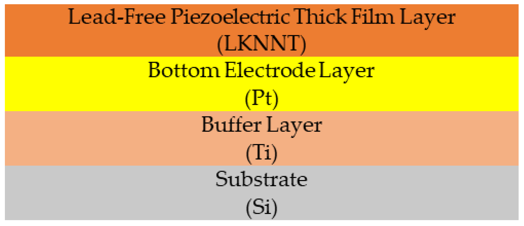
Lead-Free Piezoelectric Ceramic Micro-Pressure Thick Films

Abstract
:1. Introduction
2. Experimental Detail
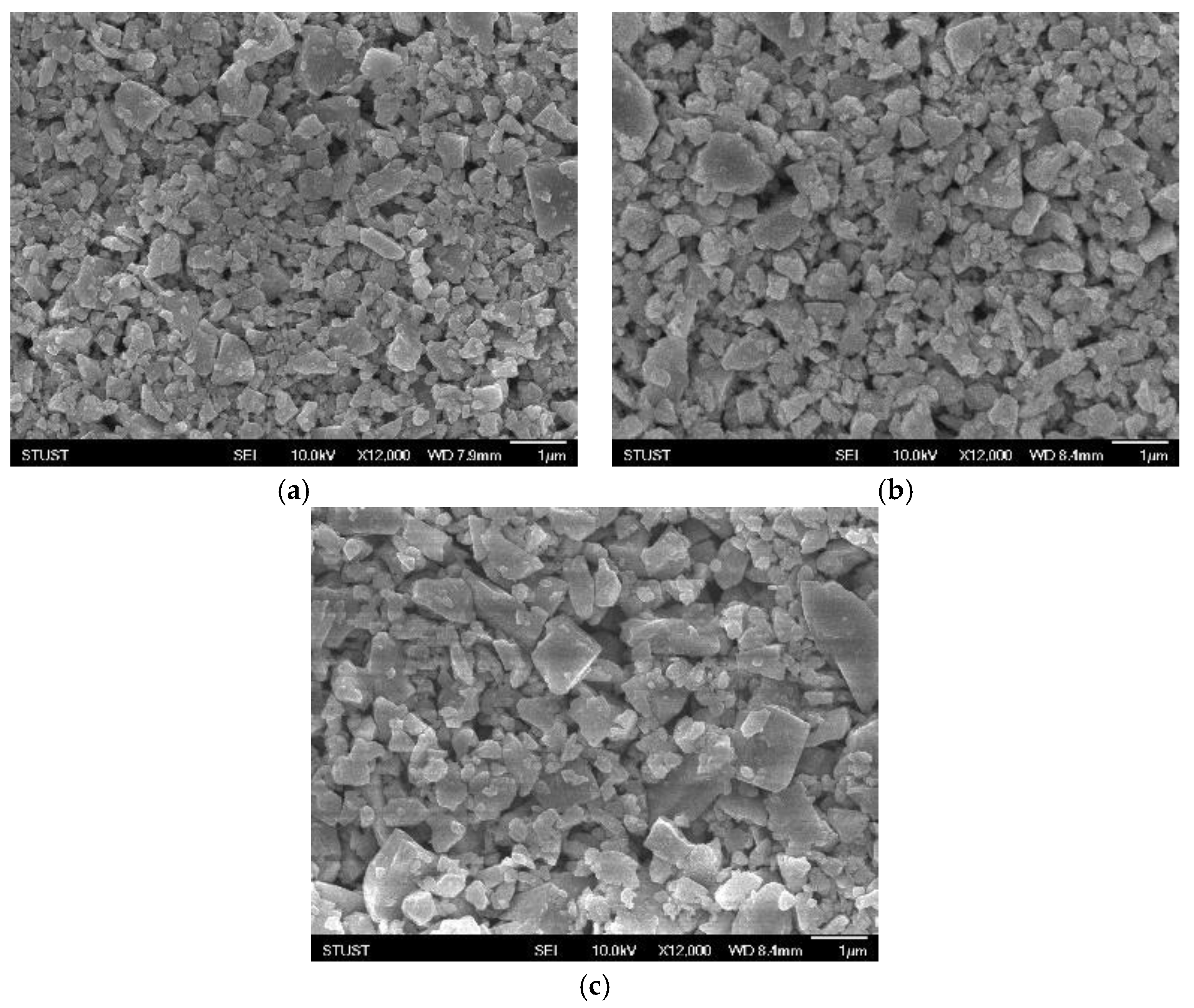
3. Results and Discussion
4. Conclusions
Author Contributions
Funding
Data Availability Statement
Conflicts of Interest
References
- Guan, T.T.; Yang, F.; Wang, W.; Huang, X.; Jiang, B.; Zhang, D.C. The Design and Analysis of Piezoresistive Shuriken-Structured Diaphragm Micro-Pressure Sensors. J. Microelectromech. Syst. 2017, 26, 206–214. [Google Scholar] [CrossRef]
- Lee, D.; Lee, H.; Jeong, Y.; Ahn, Y.; Nam, G.; Lee, Y. Highly Sensitive, Transparent, and Durable Pressure Sensors Based on Sea-Urchin Shaped Metal Nanoparticles. Adv. Mater. 2016, 28, 9364–9369. [Google Scholar] [CrossRef] [PubMed]
- Pandey, V.; Mandal, A.; Sisle, S.; Gururajan, M.; Dusane, R. Piezoresistive pressure sensor using nanocrystalline silicon thin film on flexible substrate. Sens. Actuators A Phys. 2020, 316, 112372. [Google Scholar] [CrossRef]
- Xu, T.; Wang, H.; Xia, Y.; Zhao, Z.; Huang, M.; Wang, J.; Zhao, L.; Zhao, Y.; Jiang, Z. Piezoresistive pressure sensor with high sensitivity for medical application using peninsula-island structure. Front. Mech. Eng. 2017, 12, 546–553. [Google Scholar] [CrossRef]
- Barlian, A.A.; Park, W.; Mallon, J.; Rastegar, A.; Pruitt, B.L. Review: Semiconductor Piezoresistance for Microsystems. Proc. IEEE 2009, 97, 513–552. [Google Scholar] [CrossRef] [PubMed] [Green Version]
- Fiorillo, A.; Critello, C.; Pullano, S. Theory, technology and applications of piezoresistive sensors: A review. Sens. Actuators A Phys. 2018, 281, 156–175. [Google Scholar] [CrossRef]
- Liu, D.; Liu, H.; Liu, J.; Hu, F.; Fan, J.; Wu, W.; Tu, L. Temperature Gradient Method for Alleviating Bonding-Induced Warpage in a High-Precision Capacitive MEMS Accelerometer. Sensors 2020, 20, 1186. [Google Scholar] [CrossRef] [Green Version]
- Matko, V.; Milanovic, M. Temperature-compensated capacitance–frequency converter with high resolution. Sens. Actuators A Phys. 2014, 220, 262–269. [Google Scholar] [CrossRef] [Green Version]
- Smith, A.D.; Niklaus, F.; Paussa, A.; Vaziri, S.; Fischer, A.; Sterner, M. Electromechanical piezoresistive sensing in suspended graphene films. Nano Lett. 2013, 13, 3237–3242. [Google Scholar] [CrossRef]
- Janssens, S.D.; Drijkoningen, S.; Haenen, K. Ultra-thin nanocrystalline diamond films as pressure sensors for harsh environments. Appl. Phys. Lett. 2014, 104, 073107. [Google Scholar] [CrossRef]
- Wang, J.; Chuai, R.; Yang, L.; Dai, Q. A surface micromachined pressure sensor based on polysilicon nanofilm piezoresistors. Sens. Actuators A Phys. 2015, 228, 75–81. [Google Scholar] [CrossRef]
- Gao, F.; Cheng, L.; Hong, R.; Liu, J.; Wang, C.; Tian, C. Crystal Structure and Piezoelectric Properties of xPb(Mn1/3Nb2/3)O3—(0.2-x)Pb(Zn1/3Nb2/3)O3—0.8Pb(Zr0.52Ti0.48)O3 Ceramics. Ceram. Int. 2009, 35, 1719–1723. [Google Scholar] [CrossRef]
- Yang, Z.; Chao, X.; Zhang, R.; Chang, Y.; Chen, Y. Fabrication and electrical characteristics of piezoelectric PMN–PZN–PZT ceramic transformers. Mater. Sci. Eng. B 2007, 138, 277–283. [Google Scholar] [CrossRef]
- Yang, Z.; Zong, X.; Li, H.; Chang, Y. Structure and Electrical Properties of New Pb(Zr,Ti)O3—Pb(Fe2/3W1/3)O3—Pb(Mn1/3Nb2/3)O3 Ceramics. Mater. Lett. 2005, 59, 3476–3480. [Google Scholar] [CrossRef]
- Zuo, R.Z.; Fang, X.; Ye, C. Phase Structures And Electrical Properties of new Lead-Free (Na0.5K0.5)NbO3—(Bi0.5Na0.5)TiO3 Ceramics. Appl. Phys. Lett. 2007, 90, 092904. [Google Scholar] [CrossRef]
- Wu, J.; Xiao, D.; Wu, W.; Zhu, J.; Wang, J. Effect of Dwell Time During Sintering on Piezoelectric Properties of (Ba0.85Ca0.15)(Ti0.9Zr0.1)O3 Lead-Free Ceramics. J. Alloys Comp. 2011, 509, L359–L361. [Google Scholar] [CrossRef]
- Su, S.; Zuo, R.; Lu, S.; Xu, Z.; Wang, X.; Li, L. Poling Dependence and Stability of Piezoelectric Properties of Ba(Zr0.2Ti0.8)O3—(Ba0.7Ca0.3)TiO3 Ceramics with Huge Piezoelectric Coefficients. Curr. Appl. Phys. 2011, 11, S120–S123. [Google Scholar] [CrossRef]
- Lin, D.M.; Kwok, K.; Lam, K.; Chan, H.L.W. Structure and Electrical Properties of K0.5Na0.5NbO3-LiSbO3 Lead-Free Piezoelectric Ceramics. J. Appl. Phys. 2007, 101, 074111. [Google Scholar] [CrossRef] [Green Version]
- Zhang, S.J.; Xia, R.; Shrout, T.; Zang, G.; Wang, J.F. Piezoelectric Properties in Perovskite 0.948(K0.5Na0.5)NbO3—0.052LiSbO3 Lead-Free Ceramics. J. Appl. Phys. 2006, 100, 104108. [Google Scholar] [CrossRef]
- Guo, Y.; Kakimoto, K.I.; Ohsato, H. Structure and Electrical Properties of Lead-Free (Na0.5K0.5)NbO3-BaTiO3 Ceramics. Jpn. J. Appl. Phy. 2004, 43, 6662–6666. [Google Scholar] [CrossRef]
- Zuo, R.; Rödel, J.; Chen, R.; Li, L. Sintering and Electrical Properties of Lead-Free Na0.5K0.5NbO3 Piezoelectric Ceramics. J. Am. Ceram. Soc. 2006, 89, 2010–2015. [Google Scholar] [CrossRef]
- Wang, K.; Zhang, B.-P.; Li, J.-F.; Zhang, L.-M. Lead-free Na0.5K0.5NbO3 piezoelectric ceramics fabricated by spark plasma sintering: Annealing effect on electrical properties. J. Electroceramics 2007, 21, 251–254. [Google Scholar] [CrossRef]
- Kang, J.K.; Lee, Y.; Heo, D.; Lee, H.; Dinh, T.H. Effect of Ta Doping on the Piezoelectric Properties of (K0.5Na0.5)NbO3 Ceramics. J. Korean Inst. Electr. Electron. Mater. Eng. 2014, 27, 292–296. [Google Scholar]
- Matsubara, M.; Yamaguchi, T.; Kikuta, K.; Hirano, S.I. Sinterability and Piezoelectric Properties of (K,Na)NbO3 Ceramics with Novel Sintering Aid. Jpn. J. Appl. Phy. 2004, 43, 7159–7163. [Google Scholar] [CrossRef]
- Lim, J.B.; Zhang, S.; Jeon, J.; Shrout, T.R. (K, Na)NbO3-Based Ceramics for Piezoelectric “Hard” Lead-Free Materials. J. Am. Ceram. Soc. 2010, 93, 1218–1220. [Google Scholar] [CrossRef]
- Wu, J.; Wang, Y.; Xiao, D.; Zhu, J.; Yu, P.; Wu, L.; Wu, W. Piezoelectric Properties of LiSbO3-Modified (K0.48Na0.52)NbO3 Lead-Free Ceramics. Jpn. J. Appl. Phy. 2007, 46, 7375. [Google Scholar] [CrossRef]
- Zhou, J.J.; Li, J.; Wang, K.; Zhang, X.W. Phase Structure and Electrical Properties of (Li, Ta)-Doped (K,Na)NbO3 Lead-Free Piezoceramics in the Vicinity of Na/K = 50/50. J. Mater. Sci. 2011, 46, 5111–5116. [Google Scholar] [CrossRef]
- Nakashima, Y.; Sakamoto, W.; Maiwa, H.; Shimura, T.; Yogo, T. Lead-Free Piezoelectric (K, Na)NbO3 Thin Films Derived from Metal Alkoxide Precursors. Jpn. J. Appl. Phy. 2007, 46, L311–L313. [Google Scholar] [CrossRef]
- Yu, Q.; Li, J.; Sun, W.; Zhou, Z.; Xu, Y.; Xie, Z.; Lai, F.P. Electrical Properties of K0.5Na0.5NbO3 Thin Films Grown on Nb:SrTiO3 Single-Crystalline Substrates with Different Crystallographic Orientations. J. Appl. Phys. 2013, 113, 024101. [Google Scholar] [CrossRef]
- Li, T.; Wang, G.; Li, K.; Du, G.; Chen, Y.; Zhou, Z.; Rémiens, D.; Dong, X. Electrical properties of lead-free KNN films on SRO/STO by RF magnetron sputtering. Ceram. Int. 2013, 40, 1195–1198. [Google Scholar] [CrossRef]
- Han, G.; Ryu, J.; Ahn, C.-W.; Yoon, W.-H.; Choi, J.-J.; Hahn, B.-D.; Kim, J.-W.; Choi, J.-H.; Park, D.-S. High Piezoelectric Properties of KNN-Based Thick Films with Abnormal Grain Growth. J. Am. Ceram. Soc. 2012, 95, 1489–1492. [Google Scholar] [CrossRef]
- Nguyen, M.D.; Dekkers, M.; Houwman, E.; Vu, H.; Vu, H.; Rijnders, G. Lead-Free (K0.5Na0.5)NbO3 Thin Films by Pulsed Laser Deposition Driving MEMS-Based Piezoelectric Cantilevers. Mater. Lett. 2016, 164, 413–416. [Google Scholar] [CrossRef]
- Pavlič, J.; Malič, B.; Rojac, T. Small Reduction of the Piezoelectric d33 Response in Potassium Sodium Niobite Thick Film. J. Am. Ceram. Soc. 2014, 95, 1497–1503. [Google Scholar] [CrossRef]
- Wang, L.; Yao, K.; Ren, W. Piezoelectric K0.5Na0.5NbO3 thick films derived from polyvinylpyrrolidone-modified chemical solution deposition. Appl. Phys. Lett. 2008, 93, 092903. [Google Scholar] [CrossRef]
- Goh, P.C.; Yao, K.; Chen, Z. Lead-free piezoelectric (K0.5Na0.5)NbO3 thin films derived from chemical solution modified with stabilizing agents. Appl. Phys. Lett. 2010, 97, 102901. [Google Scholar] [CrossRef]
- Matko, V.; Milanovic, M. Detection Principles of Temperature Compensated Oscillators with Reactance Influence on Piezoelectric Resonator. Sensors 2020, 20, 802. [Google Scholar] [CrossRef] [PubMed]


| Structure | Sputtering Time (Hour) | RTA Temp. (°C) | Film Thickness (nm) | Thickness Ratio (%) |
|---|---|---|---|---|
| Ti/Si | 1 | None | 50.4 | ±0 |
| 300 | 59.92 | +19 | ||
| 500 | 51.36 | +2 | ||
| 700 | 42.8 | −15 | ||
| 2 | None | 205.4 | ±0 | |
| 300 | 162.6 | −21 | ||
| 500 | 162.6 | −21 | ||
| 700 | 179.8 | −13 |
| Structure | Sputtering Time (Hour) | RTA Temp. (°C) | Pt Thickness (nm) | Thickness Ratio (%) |
|---|---|---|---|---|
| Pt/Si | 1 | None | 470.8 | ±0 |
| 300 | 445.1 | −6 | ||
| 500 | 385.2 | −18 | ||
| 700 | 368.1 | −22 |
| Structure | Sputtering Time (Hour) | RTA Temp. (°C) | Film Thickness (nm) | Thickness Ratio (%) | ||
|---|---|---|---|---|---|---|
| Pt/Ti/Si | Pt = 1 h Ti = 2 h | Ti | Pt | Ti | Pt | |
| None | 256.8 | 325.3 | ±0 | |||
| 300 | 291.0 | 325.3 | +13 | ±0 | ||
| 500 | 273.9 | 376.6 | +7 | +16 | ||
| 700 | 214.0 | 368.1 | −17 | +13 | ||
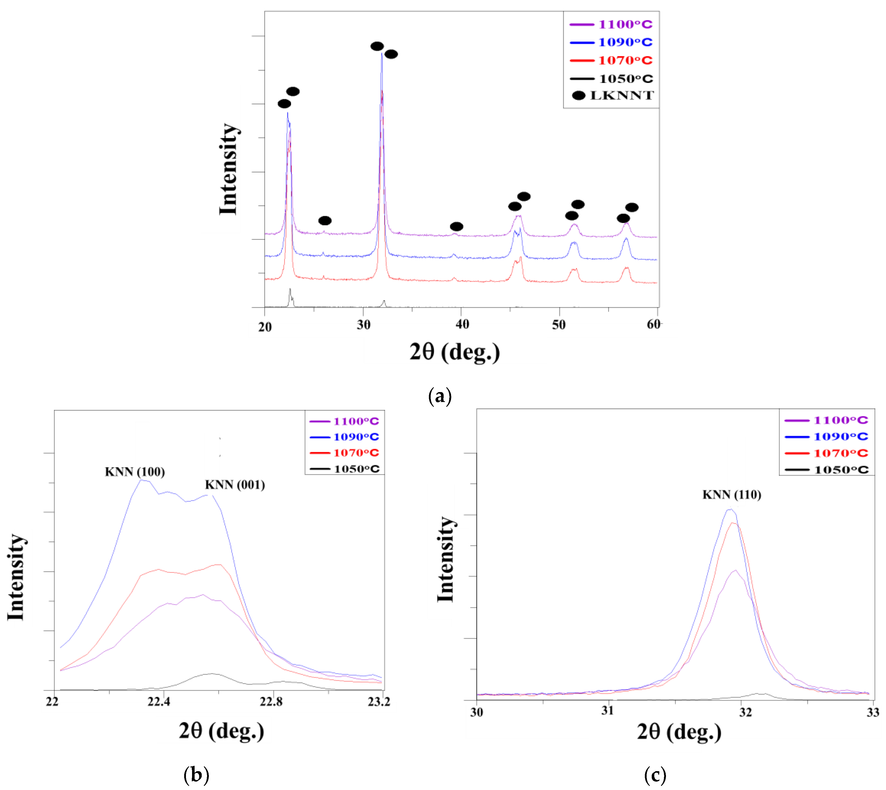
| Sintering (°C) | 1050 | 1070 | 1090 | 1110 |
|---|---|---|---|---|
| A(100)/Atotal | 0.730 | 0.349 | 0.320 | 0.317 |
| FWHM (100) | 0.198 | 0.509 | 0.462 | 0.525 |
| FWHM (001) | 0.184 | |||
| A(110)/Atotal | 0.270 | 0.410 | 0.402 | 0.407 |
| FWHM (110) | 0.301 | 0.456 | 0.423 | 0.506 |
| Lattice constant (10−8 cm) | 3.942 | 3.961 | 3.968 | 3.959 |
| Theoretical density (g/cm3) | 4.882 | 4.811 | 4.789 | 4.819 |
| Method | Pressureless Sintering | Solid-State Reaction |
|---|---|---|
| Elasticity interval (μm) | 2 | 1.25 |
| Critical stress/deformation (mN/nm) | 3.38/2133 | 3.01/1411 |
| Young’s modulus (GPa) | 3.629 | 13.126 |
| Hardness (MPa) | 32.528 | 60.554 |
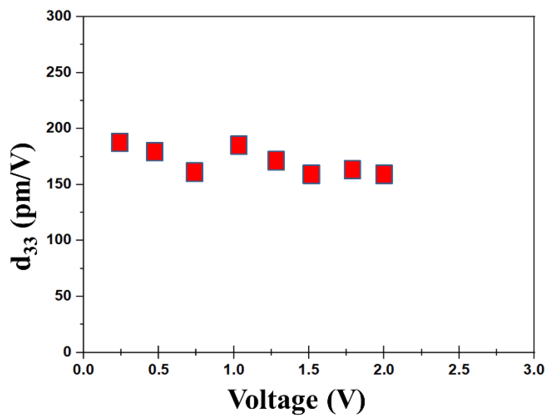
| Material System | Method | d33 |
|---|---|---|
| KNN | Chemical Solution Deposition | 46 pm/V |
| KNN | Sol-Gel Method | 50 pm/V |
| KNN | RF Magnetron Sputtering | 36 pm/V |
| KNN | Pulsed Laser Deposition | 58 pm/V |
| KNN | Screen Printing Method | 138 pm/V |
| KNN | Chemical Solution Deposition | 61 pm/V |
Disclaimer/Publisher’s Note: The statements, opinions and data contained in all publications are solely those of the individual author(s) and contributor(s) and not of MDPI and/or the editor(s). MDPI and/or the editor(s) disclaim responsibility for any injury to people or property resulting from any ideas, methods, instructions or products referred to in the content. |
© 2023 by the authors. Licensee MDPI, Basel, Switzerland. This article is an open access article distributed under the terms and conditions of the Creative Commons Attribution (CC BY) license (https://creativecommons.org/licenses/by/4.0/).
Share and Cite
Chen, K.-H.; Cheng, C.-M.; Chen, Y.-J.; Chen, M.-L. Lead-Free Piezoelectric Ceramic Micro-Pressure Thick Films. Crystals 2023, 13, 201. https://doi.org/10.3390/cryst13020201
Chen K-H, Cheng C-M, Chen Y-J, Chen M-L. Lead-Free Piezoelectric Ceramic Micro-Pressure Thick Films. Crystals. 2023; 13(2):201. https://doi.org/10.3390/cryst13020201
Chicago/Turabian StyleChen, Kai-Huang, Chien-Min Cheng, Ying-Jie Chen, and Mei-Li Chen. 2023. "Lead-Free Piezoelectric Ceramic Micro-Pressure Thick Films" Crystals 13, no. 2: 201. https://doi.org/10.3390/cryst13020201