Article

The Study of the Wrinkles of Hexagonal Boron-Nitride Flake after the Annealing

1
Department of Mechanical Engineering, Anyang Institute of Technology, Yellow River Avenue West, Anyang 455000, China
2
School of Accountancy, Anyang Institute of Technology, Yellow River Avenue West, Anyang 455000, China
*
Author to whom correspondence should be addressed.
Crystals 2023, 13(2), 304; https://doi.org/10.3390/cryst13020304
Submission received: 9 January 2023 / Revised: 7 February 2023 / Accepted: 9 February 2023 / Published: 12 February 2023
(This article belongs to the Section Materials for Energy Applications)

Abstract

:
Hexagonal boron nitride (h-BN) flakes have been widely used due to their excellent physical and chemical properties. Here, thermal-induced wrinkles of thin h-BN flakes deposited on silicon dioxide substrate were investigated through a combination of atomic force microscopy (AFM) and Raman spectroscopy. The experimental results indicated that the wrinkles did not occur at relatively low annealing temperatures and were detected at temperatures as high as 500 °C or even 600 °C. When repeatedly annealed at high temperatures, the number and positions of the wrinkles also changed. From the Raman spectra, the wrinkles were caused by the fact that the h-BN contraction rate was faster than that of the substrate at the cooling stage due to the interfacial sliding between the flake and the substrate and the h-BN flake of 7 nm thickness recovered to the original length at 150 °C. Further cooling introduced the compressive stress and then the wrinkles appeared. Moreover, it was found that if there was a crack in the h-BN flake, the wrinkle always appeared at the crack. Our findings appeal the mechanism of thermal-induced wrinkles of h-BN flakes and help us to research their applications as substrate materials in electronic devices in a high-temperature environment.

1. Introduction

In 2004, the Geim group successfully separated graphene, which has aroused scholars’ research upsurge in two-dimensional nanomaterials [1]. Two-dimensional nanomaterials refer to layered materials with a transverse size greater than 100 nm but only a few atoms thick or even a single atom. In recent years, two-dimensional materials have been widely used in optoelectronic devices [2], catalysis [3] and batteries [4] because of their excellent physical and chemical properties.
Hexagonal boron nitride (h-BN) flakes, as a representative of two-dimensional materials, have a similar crystal structure to graphene and their own excellent thermal conductivity [5], high temperature resistance [6], oxidation resistance [7] and high dielectric properties [8]. h-BN flakes have been used in many fields, such as a heterojunction with graphene [9], anticorrosion [10] and reinforced composites [11]. However, many of these applications are in high-temperature conditions. Therefore, it is very important to study the structural changes and physical properties of h-BN nanocrystals at high temperatures. Most of the objects have a positive coefficient of thermal expansion (CTE), indicating that they will be stretched or compressed when heating or cooling, but the CTE of h-BN flakes is negative [12]. Therefore, when the h-BN flakes are transferred to materials with positive CTE, the mismatch of thermal expansion mismatches leads to interfacial shear force. The shear force can lead to the wrinkles of nanocrystals of h-BN flakes during a heating and cooling cycle [13], which has a potential effect on the application stability of h-BN flakes in micro- and nanodevices. Moreover, the wrinkles can strongly affect the physical properties of such two-dimensional materials [14,15,16,17]. Additionally, the wrinkles can form potential edgeless nanocapillaries for the transport of ions and molecules [18,19,20].
Many researchers have found that wrinkles in the two-dimensional materials always occur during the sample preparation and transfer process or under compressive and shear stresses. The periodic and random orientation wrinkles were produced [13,17,21,22], which may be attributed to the Poisson’s ratio effect during the loading/unloading cycle, as well as the influence of lamellar geometry and tensile strain directivity of two-dimensional materials [23,24]. High temperature annealing inducing compressive stress is the main way in the study of wrinkles generation. Camilla [13] studied the wrinkle morphology of h-BN flakes with a thickness of 300 nm after annealing at 1000 °C. They found that the wrinkles were random and showed a crystal-oriented with Y-type junction morphology. The Y-type wrinkles were also found in other two-dimensional materials, such as graphene, GaS, MoS2 and WSe2 flakes [17]. Chen’s research results showed that wrinkling of h-BN flakes along the armchair direction was energetically favorable [22]. Their findings helped to evaluate the crystallographic orientation of bulk h-BN rapidly and easily. However, most of the studies ignored the relationship between the mechanism of wrinkle generation and annealing temperature. Moreover, the findings lacked the influence of self-defects on the wrinkles generation of h-BN flakes.
In this study, both ex situ and in situ Raman spectra were performed to investigate the interfacial load transfer and to reveal the generation mechanism of wrinkles of h-BN flakes after annealing at various temperatures. AFM was used in the meantime to keep track of the variations of morphology of the h-BN flakes following each heating/cooling stage. According to the results of our investigation, the slippage of the contact during the cooling stage is the primary cause of wrinkles. During the cooling stage, the shrinking rate of the h-BN was faster than the substrate, so the substrate did not reach the original size when the h-BN flake had recovered to the initial size. The substrate continued to contract as the temperature dropped, and the interfacial shear force brought the compressive stress to the sample. In order to resist this compressive stress, the surface wrinkles were generated. Furthermore, the defective h-BN flakes were compressed through molecular dynamics simulation, and it was discovered that the wrinkles had to show up where there were cracks. The Raman and AFM techniques are used to reveal the generation mechanism of wrinkles of h-BN flakes after annealing, which is helpful for their application in a high-temperature environment.

2. Materials and Methods

2.1. Sample Preparation

The h-BN flakes were prepared by mechanical cleavage of boron nitride powder (Momentive, PT110) [25]. Boron nitride powder of grade PT110 is a large single-crystal powder in the typical hexagonal platelet (graphite-like) shape. PT110 possesses an average particle size of ~45 μm. The h-BN flakes used in our study were peeled off with adhesive tape, attached to a 90 nm thick SiO2 substrate and identified by using simple optical microscopy. The sample preparation process is shown in Figure 1. First, sprinkle boron nitride powder on a tape, and then, repeatedly use the new tape to stick to the previous tape 20 times. Then, stick the last tape to the SiO2 substrate, press it hard with an eraser and finally tear the tape off. Some of h-BN flakes were found to be transferred to the substrate by means of optical imaging. The thickness of the flakes prepared was measured by an atomic force microscope. Due to the residual glue during the transfer process, the substrate was heated at 300 °C to remove the glue on the hot plate.

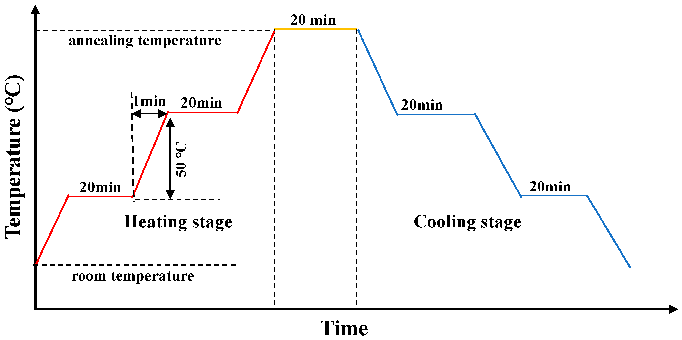
2.2. Annealing Experiment and Raman Spectra Measurement

The annealing experiments were performed by using a heating/cooling stage (Linkam TS 1500). This heating/cooling stage was linked with a Renishaw InVia Raman microscope with a 532 nm wavelength excitation laser, so the Raman spectra was collected every 50 °C change in temperature during the heating and cooling process. The Raman characterization was completed in 20 min. The schematic diagram of the annealing process is shown in Figure 2. Real-time Raman spectra at annealing temperatures of 300 °C, 400 °C, 500 °C, 600 °C and 700 °C were recorded, respectively, during the heating and cooling process. Both heating and cooling rates were set at 50 °C/min, and the sample temperature was maintained for 20 min when it rose up to the annealing temperature. An interval of 24 h between each annealing test ensured that the residual stresses were fully released.

2.3. AFM Characterization

The thickness and morphology of the h-BN flakes used in our study were identified by AFM (Park, XE-70) with closed-loop piezo stages in the tapping mode, which was housed inside an environmental chamber with a computerized humidity control. AFM is an advanced tool used to characterize sample surfaces with outstanding resolution. It eschews optical methods of microscopy in favor of a scanning probe, which comprises an extremely sharp probe tip mounted on a cantilever, as shown in Figure 3a. In tapping mode, the sharp probe tip is not scanned across the sample surface while in constant contact. Instead, the cantilever is vibrated near its resonance frequency, causing the tip to oscillate up and down. This means the probe only comes into close contact with the surface intermittently, so the surface cannot be damaged by the tip during the scanning process. Silicon nitride AFM cantilevers (AC40TS, Olympus, Tokyo, Japan) with a spring constant of 0.1 N/m and tip of curvature about 8 nm were employed in every measurement. The areas of interest were obtained and marked through an optical microscope of AFM, as shown in Figure 3b, so that they can be located more quickly by the tip of AFM. The h-BN flakes were scanned after the annealing process was done for 24 h. The resonant frequency of the cantilever was 110 kHz, and the scan frequency was set at 1 Hz.

2.4. Roughness Measurement

The arithmetic mean deviation (Ra) of the profile is used to characterize the roughness of the h-BN surface. It is usually used to characterize the roughness of the one-dimensional contour of the object surface [26]. Ra refers to the average roughness between a roughness profile and the reference line. The calculation method is as follows:
R a = ( 1 / N ) i = 1 N Z i
where Z is the distance from the point on the samle surface contour to the reference line, and N is the number of sampling points. Ra in this study was obtained through analyzing ten lines of sample AFM images by using Park Systems XEI 1.8 software.

2.5. Molecular Dynamics Simulation

The LAMMPS package was used to study the crack effect of h-BN flakes under compressive stress. The simulation model consists of crystalline silicon dioxide and bilayer h-BN flakes, in which silicon dioxide is composed of 11,657 atoms and the bilayer h-BN flakes are composed of 2880 atoms, as shown in Figure 4. A rectangular crack appears in the h-BN flake after deletion of the 10 Å× 20 Å atoms at the edge. As mentioned above, the compressive stress is caused by the thermal expansion coefficient mismatch between the h-BN flake and the substrate during the cooling process. Therefore, in order to simulate compressice stress, both sides of the bottom layer of the h-BN flake move toward the center region. The Tersoff potential is used to describe the atomic reaction in the silicon dioxide and h-BN flake layers, and the parameters are detailed in Reference [27]. The interaction of the h-BN flake inter layers uses the ilp/graphene/hbn and coul/shield potential, and the interaction between the h-BN flake and silicon dioxide layer uses van der Waals force, and the parameters are detailed in Reference [28]. The force at the bottom layer of the silicon dioxide substrate is set at zero to prevent the model from moving during the simulation. The system first relaxes for 20,000 steps under the NVT ensemble, and then, the atoms of the bottom layer on both sides move 1000 steps toward the center at a speed of 2 Å/ps, then continue to run 50,000 steps. The temperature is kept at 1 K through the Nose–Hoover thermostat, the time step is set to 0.001 ps and the total simulation time is 71 ps.

3. Results and Discussion

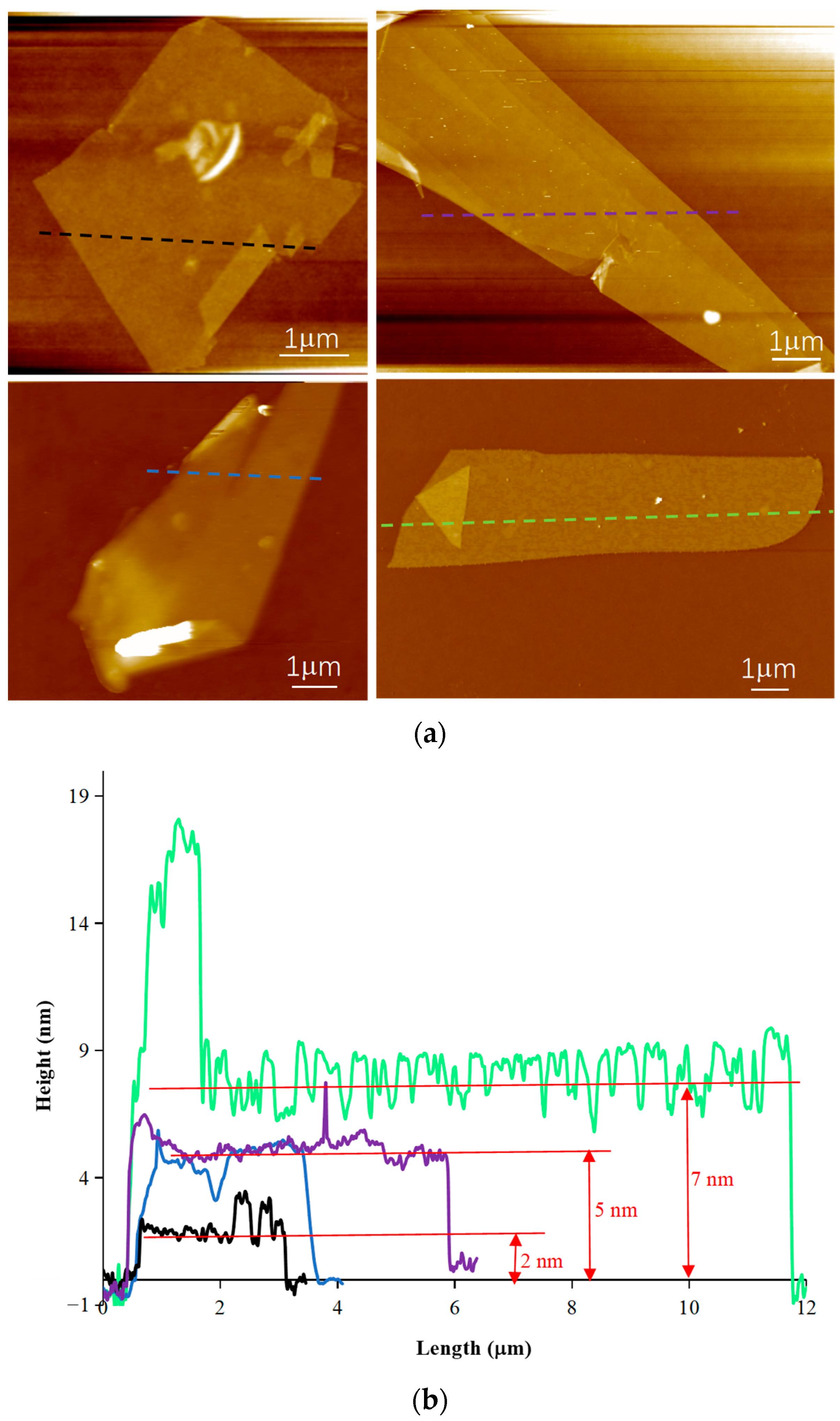
3.1. Thickness Measurement of Prepared

The h-BN flakes of different thicknesses are prepared by mechanical peeling with tape. With the aid of an optical microscope, the location and size of samples can be determined by using the color and contrast differences between the h-BN flakes and the surrounding SiO2 substrate. As shown in Figure 3b, the samples with blue color mean thinner h-BN flakes, while the samples with bright colors mean thicker h-BN flakes. The morphology of the samples is characterized by AFM. It can be seen from Figure 5a that the prepared samples have various shapes, and some samples have defects of folding or notching. The height image along the dashed lines with different colors is shown in Figure 5b. The thickness of the prepared samples ranges from 2 nm to 7 nm, corresponding to 5–20 layers by considering layer spacing of 0.34 nm [22].

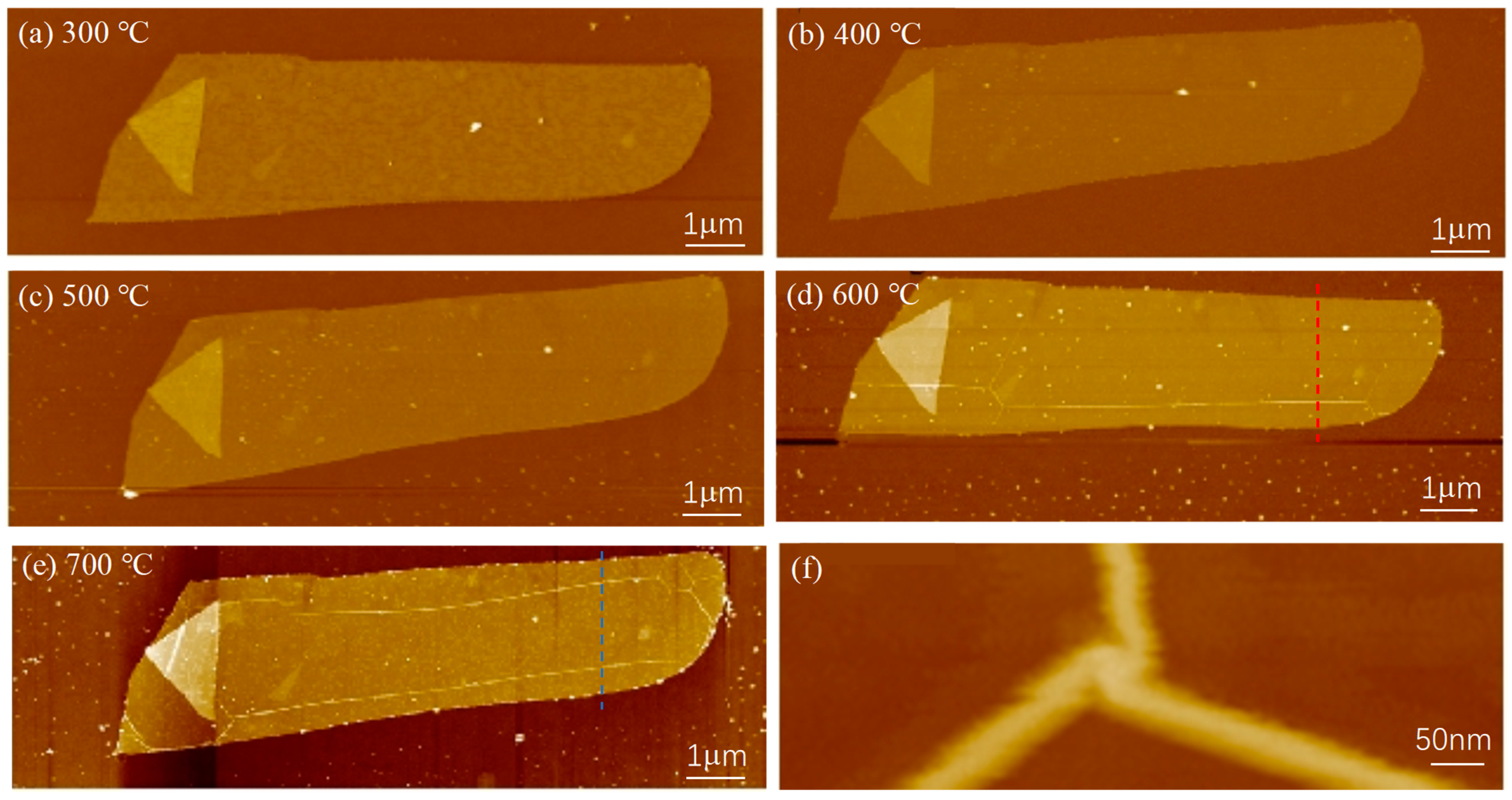
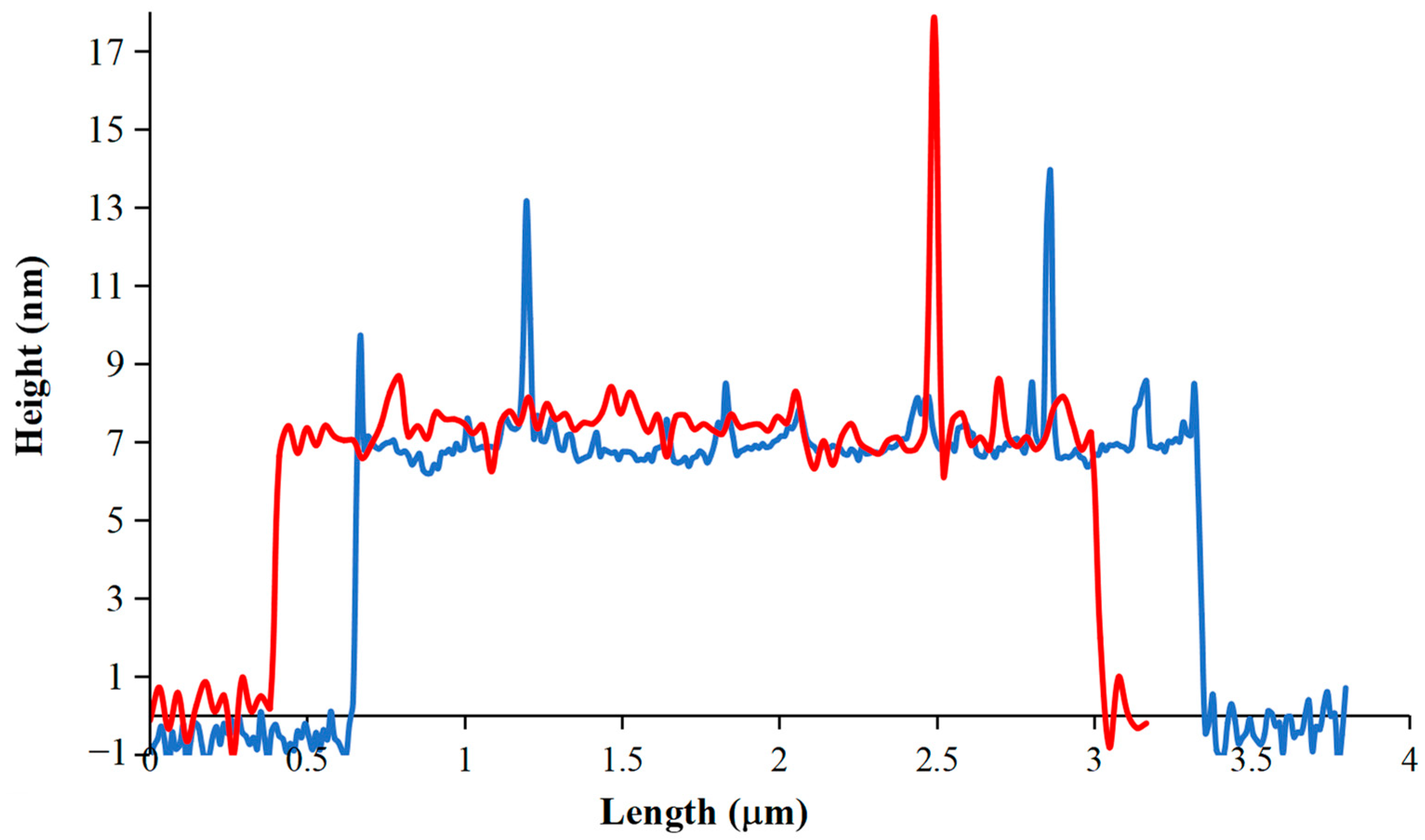
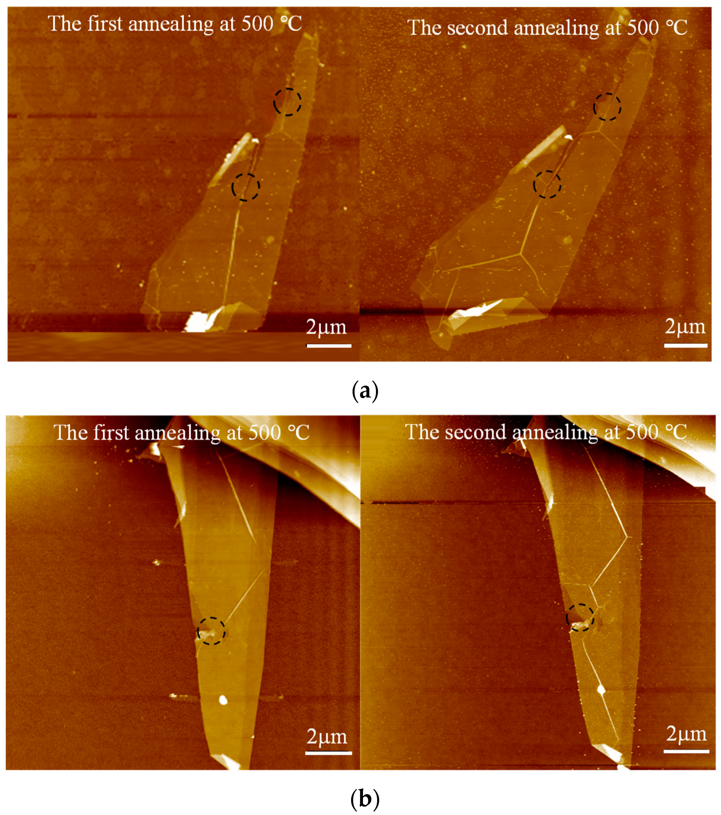
3.2. Morphology Variation after Each Annealing

The h-BN flake of 7nm thickness was chosen to observe the morphology variations after each annealing of different temperatures. Figure 6a–e show AFM images of h-BN flakes after annealing of 300 °C, 400 °C, 500 °C, 600 °C and 700 °C, respectively. As can be observed from the images, when the annealing temperature is lower than 600 °C, there is no discernible change on the sample’s surface. However, the sample’s surface starts to wrinkle as the temperature increases to 600 °C. Additionally, the wrinkles also appear in the triangular area up to 18 nm in thickness. Taking a close look at Figure 6d,e, the wrinkle connections present Y-types, as shown in Figure 6f. The angle of the cross wrinkles is about 120°, which indicates that they were created along crystallgraphic directions. This explanation has been verified by the Bernardo group [13]. It is known that h-BN has the same atomic-level flat surface and lattice structure as graphene. One possible reason lies in the annealing treatment and the differences between the thermal expansion coefficients of h-BN and silicon substrates by a mechanism similar to the wrinkling of CVD-grown and mechanically exfoliated flake graphene [17].
Although the wrinkles after annealing occurred under both 600 °C and 700 °C, their number and location changed. Two long wrinkles were observed under 700 °C, and only one long wrinkle appeared under 600 °C. The number of wrinkles grows along with the annealing temperature, suggesting that more compressive strain has been introduced. In order to verify our suspicions, the heights along the red dashed line in Figure 6d and along the blue dashed line in Figure 6e were measured, as shown in Figure 7. The wrinkle heights after annealing under 600 °C and 700 °C were approximately 6 nm and 10 nm relative to the flat sample surface. Although the winkles after annealing under 700 °C were lower than those that appeared under 600 °C, the strain corresponding to two wrinkles was greater than one wrinkle. Although there were less wrinkles at 700 °C than at 600 °C, there were more wrinkles to withstand the compressive stress at 700 °C.
In order to verify whether the generation of winkles is related to the thickness of the samples, two other samples of 5 nm thicknesses were investigated, as shown in Figure 8. Compared to the sample of 7 nm thickness above, both samples in Figure 8 had crack defects, which may have been created during the mechanical peeling process. The wrinkles are created after annealing at 500 °C. This means that the thinner the h-BN flakes, the more likely it wrinkles under the annealing-induced substrate strain. According to the St. Venant’s principle [29], the stresses in an object caused by a load distributed over a small area (or volume) of the elastomer, a little farther away from the zone of action of the load, are essentially related only to the combined force and moment of the load; the specific distribution of the load affects only the stress distribution near the zone of action of the load. The stress is so small as to be almost equal to zero at a place far from the area where the load acts. During the annealing process, the bottom layer of the h-BN flake is in direct contact with the substrate, and due to the adhesion force, shear forces are generated on the contact surface, inducing compressive stresses. The more layers there are, the more stresses can be released internally. With the same stress on the bottom, the fewer the layers, the easier it is to generate the wrinkles to release the stress.
With repeated annealing, the positions of the wrinkles changes accordingly. As shown in Figure 8a, the long wrinkle at the first annealing becomes a Y-shaped wrinkle at the second annealing. Additionally, the wrinkle in the central region in Figure 8a moves up to the left and forms a stable Y-shape when it meets with the other wrinkle above. More Y-shaped wrinkles appear after the second annealing. This means that wrinkles along the lattice direction are more stable, while long wrinkles tend to move or even disappear when the repeated annealing results in a change in the stress state. Moreover, it was found that if there was a crack in the sample, then there must be wrinkles at the crack, and the wrinkles would not disappear after repeated annealing. This is because the crack position tends to lead to stress concentration [30]. The uniform load suddenly encounters a region with a smaller cross-section during transmission, resulting in an increase of stress, so the wrinkles are generated to release the stress. It is interesting to note that there is an impurity in Figure 8b, and the wrinkle appears and goes through it. This defect of impurity also tends to cause stress concentration.

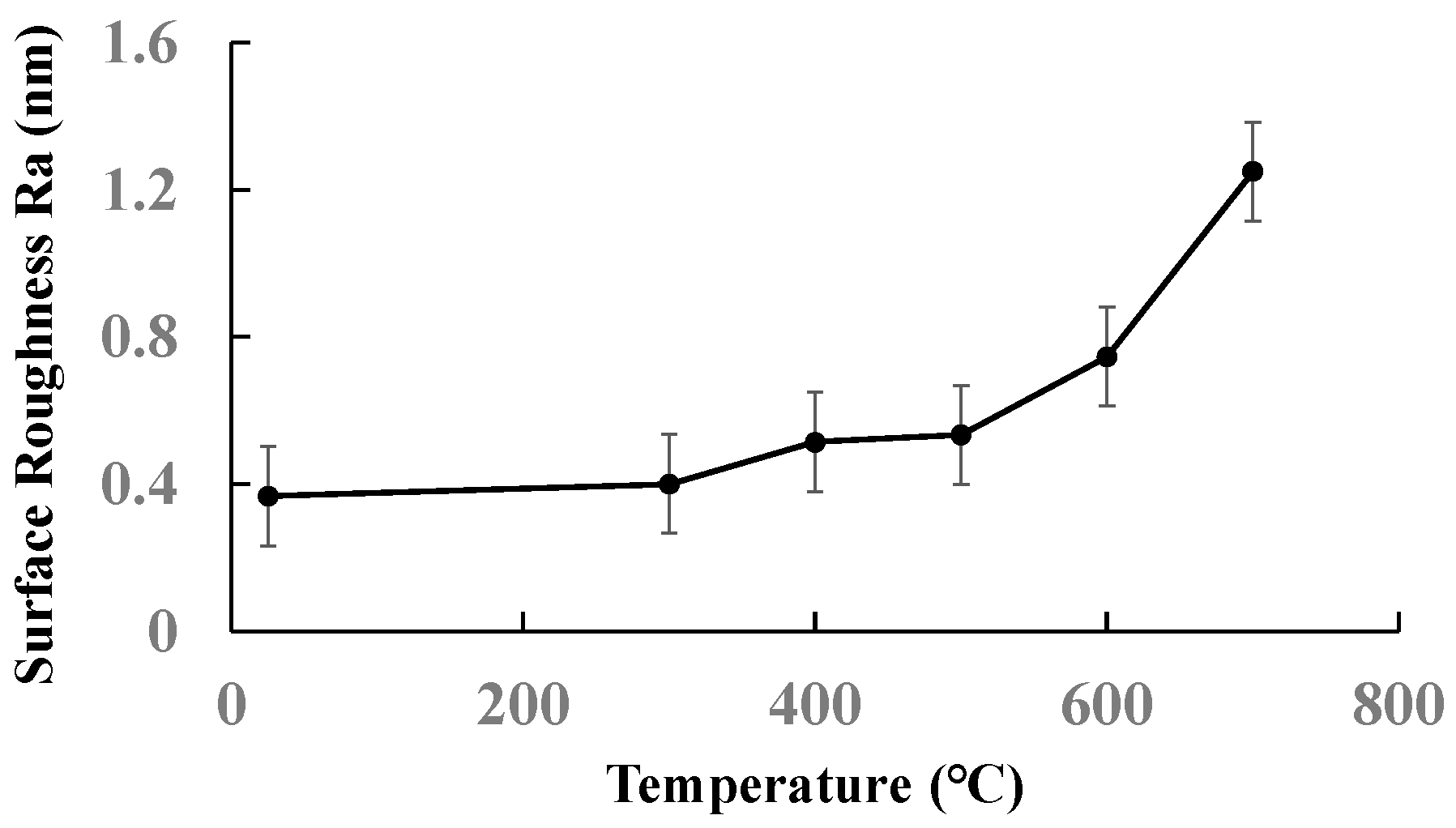
3.3. Surface Roughness

The surface roughness of the sample of 7 nm thickness can be obtained directly from the above AFM images (Figure 6), as shown in Figure 9. The roughness of ten lines in different areas of the h-BN flake was investigated after annealing at different temperatures. It can be seen from Figure 9 that the surface roughness of the sample is about 0.4 nm at room temperature and 300 °C. Before 500 °C, the roughness of the sample is kept in a narrow range of about 0.3–0.6 nm. However, when the annealing temperature reaches 600 °C, the surface roughness suddenly increases, and the roughness rises to 0.7 nm. Finally, when the temperature reaches 700 °C, the roughness is 1.2 ± 0.15 nm. This is consistent with the fact that wrinkles are observed in Figure 6. The roughness of the h-BN flake surface depends on the atomic lattice match between boron nitride and the silicon dioxide substrate. The higher the temperature, the more severe the lattice mismatch will be. The thin h-BN flakes are reported to have a negative in-plane thermal expansion coefficient compared to the positive thermal expansion coefficient of silicon oxide substrates. This means that h-BN flakes shrink at higher temperatures, which leads to more pronounced winkles and a higher surface roughness.

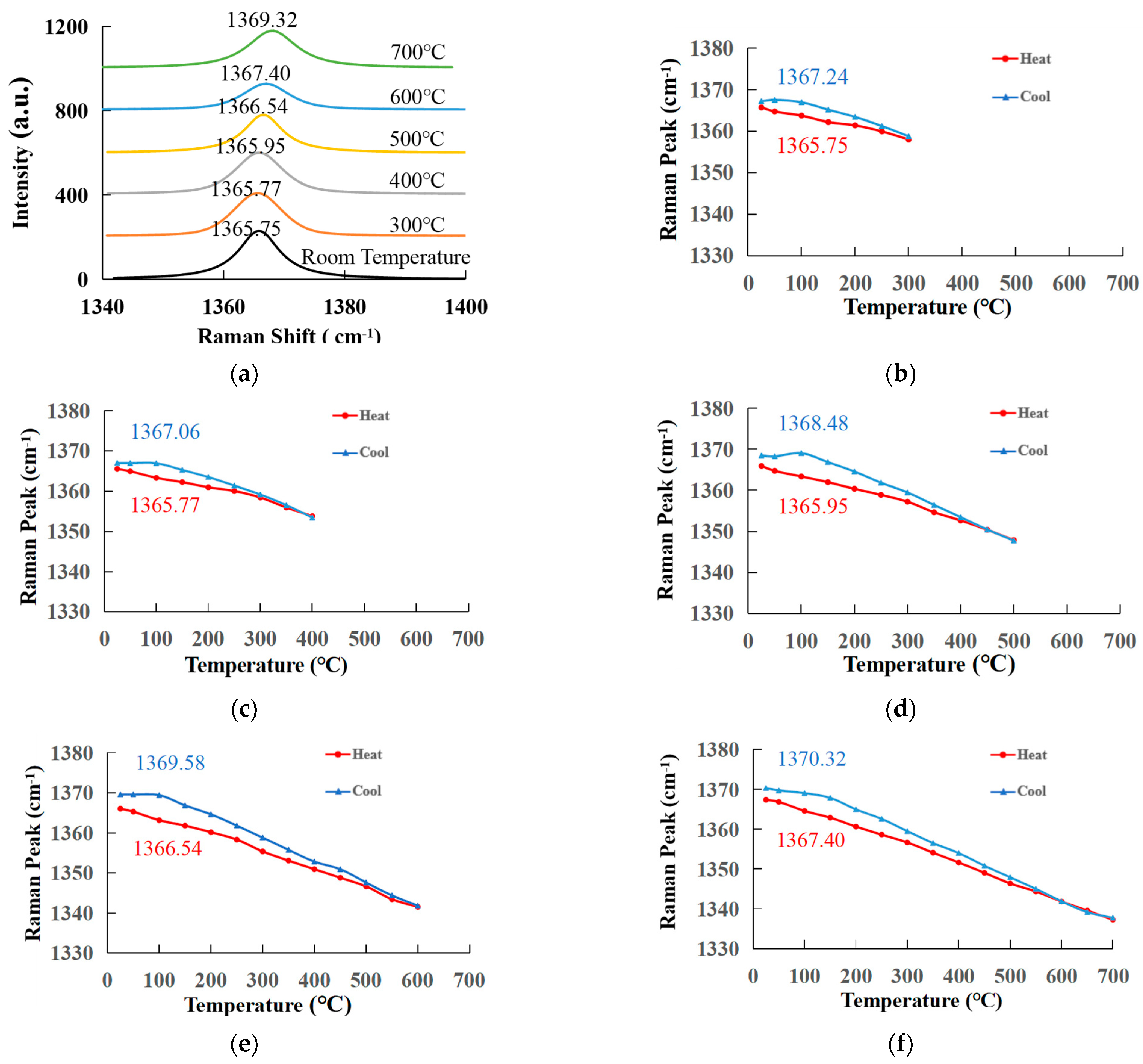
3.4. Ex Situ and In Situ Raman Spectra
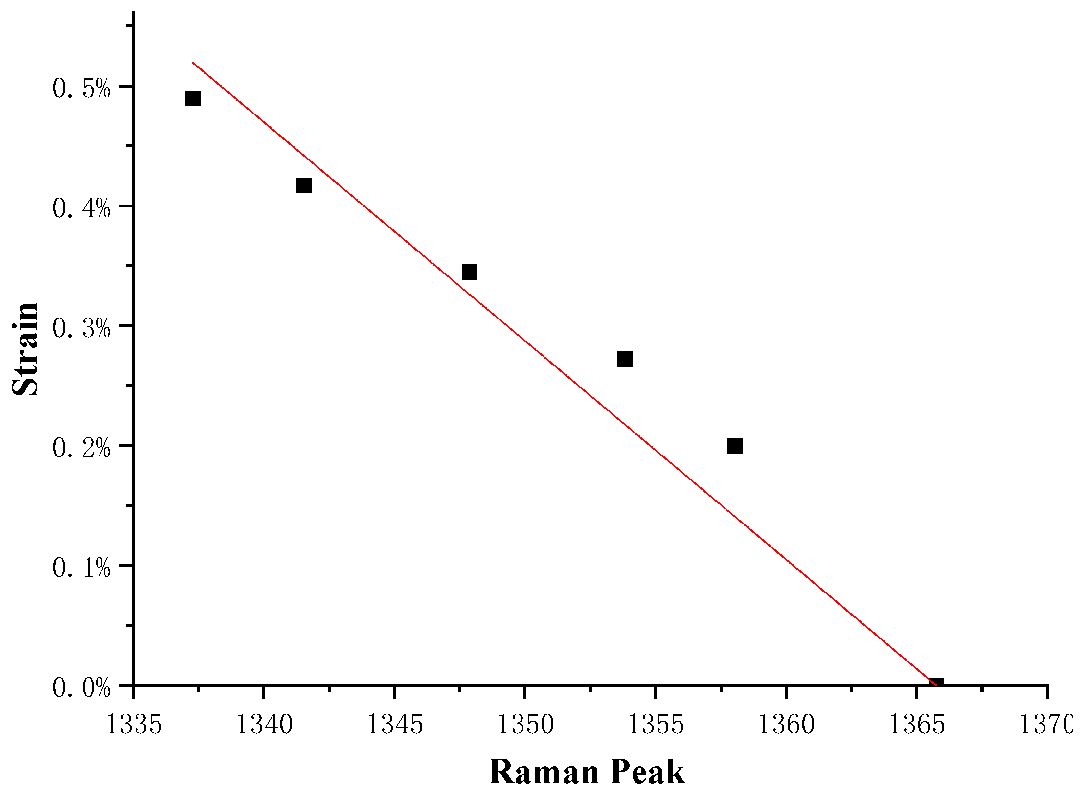
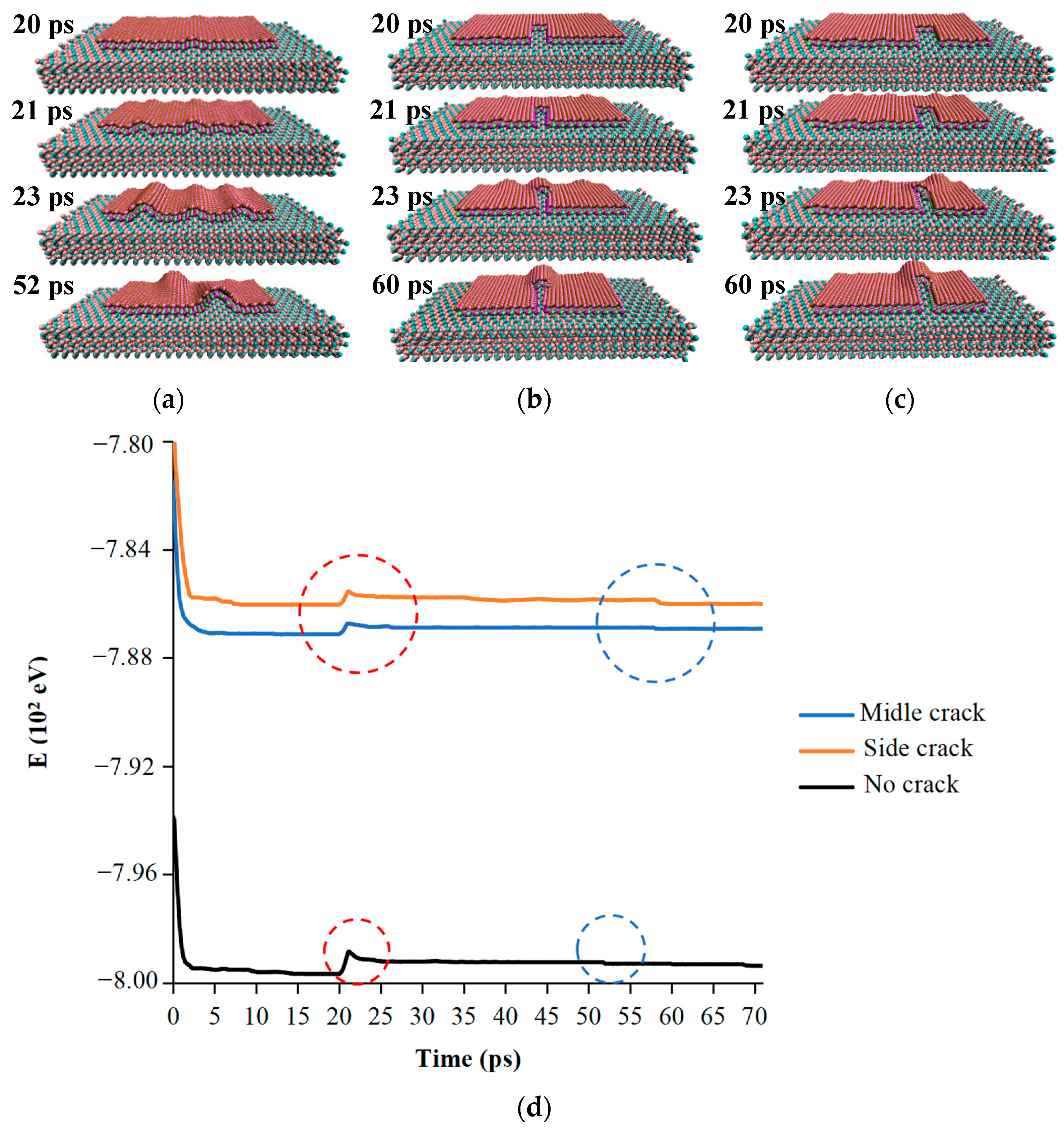
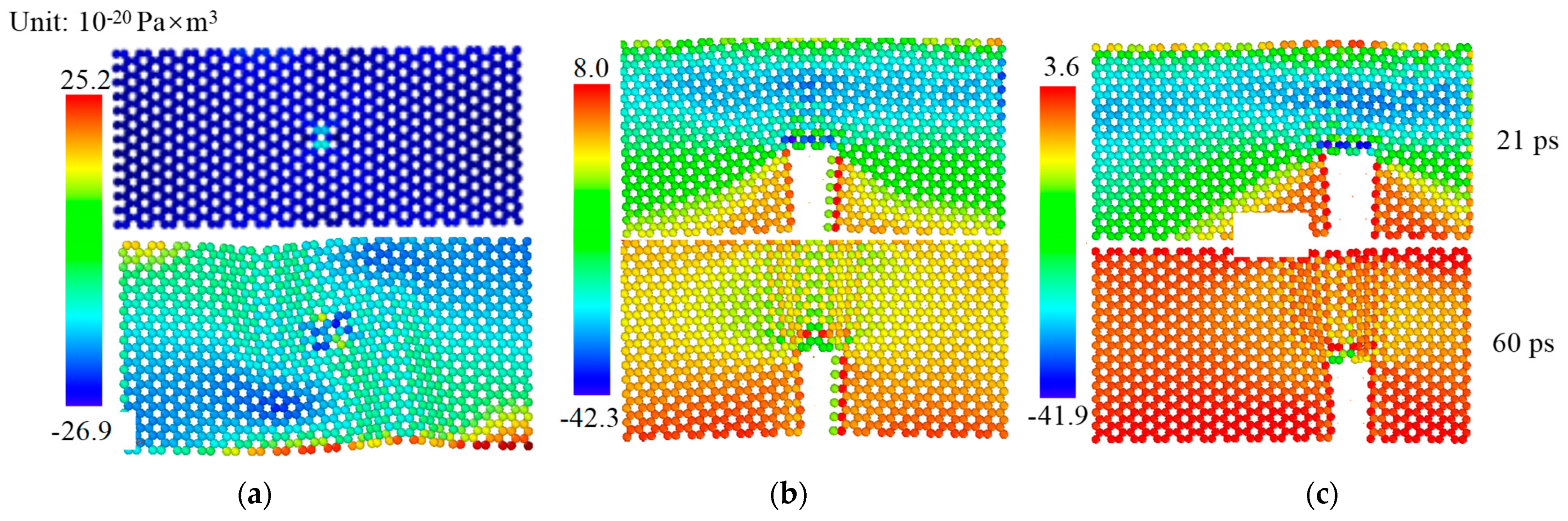
It is now well established that Raman spectroscopy can be used to follow stress transfer in two-dimensional materials [31,32]. The Raman peak shift originating from the E2g mode of BN vibrations can deflect the in-plane strain of the h-BN flakes according to many other literature [17,33]. The left shift of the peak of h-BN represents the introduction of tensile stress, and the right shift represents the introduction of compressive stress. Figure 10a shows the ex situ Raman spectra of the sample shown in Figure 6 after annealing at different temperatures. Each ex situ Raman measurement was performed 24 h after annealing. The initial Raman peak of the sample is 1365.75 cm−1 at room temperature, as shown in Figure 10a. The E2g mode was centered at ∼1365 cm−1, the expected value for bulk h-BN [34], suggesting that no stress was induced in our sample prepared process. When the annealing temperature is below 500 °C, there is no obvious shift of the Raman peak. This shows that there is no large sliding between the sample and the substrate below 500 °C and no introduction of compressive stress. When it reaches 600 °C, the peak rises to 1367.40 cm−1. Continuing to increase the temperature to 700 °C, the peak rises to 1369.32 cm−1. Compared with the initial Raman peak of 1365.75 cm−1, the difference after annealing at 300 °C, 400 °C, 500 °C, 600 °C and 700 °C, are 0.02 cm−1, 0.20 cm−1, 0.79 cm−1, 1.65 cm−1 and 3.57 cm−1, respectively. These values are measured when the sample has cooled for 24 h after annealing, so the change in the Raman peak is permanent. These permanent Raman peak shifts indicate that h-BN flakes produce irrecoverable mechanical deformations at high temperature annealing. The wrinkles in the h-BN flake of 7 nm thickness appears after annealing at 600 °C, which implies that the compressive stress needs to make the Raman peak shift at least 1.65 cm−1 before the wrinkles are produced. Even though the wrinkles are not observed at low temperature annealing, it still introduces compressive stress from the variations of the Raman peak, but the introduced compressive stress is just not enough to generate wrinkles.
The Raman peak shifts in situ can be seen in Figure 10 b–f during the heating and cooling cycle at different annealing temperatures. Raman spectra and their Raman peak are found to shift with stress, which enables stress transfer to be monitored between the h-BN flake and SiO2 substrate. By analyzing the peak shift–temperature relationship curve, stress variations of the h-BN flake during the heating and cooling cycle are emphasized. During the heating stage, the frequency shifts of the Raman peak display a linear downshift as the temperature rises, which indicates that the elastic tensile stress is effectively transferred to the h-BN flake by the interfacial shear. Although the h-BN flake has a negative coefficient of thermal expansion, it is actually in a stretched state instead of compression due to the strong adhesion between the bottom layer of the h-BN flake and the silicon dioxide substrate when the temperature increases. During the cooling stage, the frequency shifts of the Raman peak display a two-stage upshift trend. At the start, the frequency shifts of the Raman peak move upward linearly. Notice that the frequency upshift rate during cooling is higher than the downshift rate during heating. This is because the sample was maintained for 20 min at the annealing temperature, and the high temperature can weaken the Van der Waals force between the substrate and the sample [35], resulting in interfacial slippage. However, when the temperature has not dropped to room temperature yet, the Raman peak has reached the initial value, which indicates that the stress of the sample has returned to its original state. As the temperature continues to cool, new compressive stresses are introduced. Then, the frequency change enters a plateau stage. For example, in Figure 10f, the initial peak is 1367.40 cm−1 and drops to 1337.75 cm−1 when the temperature rises to 700 °C. Then, when the temperature cools to 150 °C, it returns to 1367.86 cm−1. As the temperature continues to cool to 100 °C, the Raman peak rises to 1369.06 cm−1. The temperature continues to cool, and the frequency changes little or even decreases. The thermal contraction of the substrate as a result of the temperature decrease induces an in-plane compress force to the bottom layer of the h-BN flake, and the whole h-BN sheet is contracted through the interlayer binding interactions, which, in turn, leads to the creation of wrinkles to release the compressive stress. Thus, it is concluded that the h-BN flake wrinkles during the 600 °C and 700 °C annealing begin to generate when the temperature cools to 100 °C.
The red and blue numbers in Figure 10 represent the Raman peak frequency at room temperature before and after annealing. The differences between the two values after annealing at 300 °C, 400 °C, 500 °C, 600 °C and 700 °C were 1.49 cm−1, 1.29 cm−1, 2.53 cm−1, 3.04 cm−1 and 2.92 cm−1, respectively. It is worth noting that the Raman peak frequency of h-BN at room temperature in situ after annealing is a little higher than that of ex situ. This is because the measurements in situ were carried out after cooling down for 20 min, and the interior of the material was not completely stabilized. The ex situ measurements were performed 24 h after the return, and the internal stress was basically completely released.
In order to obtain the relationship between the Raman peak frequency shift and the strain of the boron nitride, it is assumed here that there is no strain induced in the sample prepared process. The strain in the h-BN flake at temperature t is calculated as Δ ε ( t ) = ( C T E S i O 2 C T E B N ) × ( t 25 ° C ) , where C T E S i O 2 = 0.56 × 10 6 / ° C is the coefficient of thermal expansion of SiO2 [36] and C T E B N = ( 2.3 × 10 12 t 2 + 5.2 × 10 9 t 6.7 × 10 6 ) / ° C is the coefficient of thermal expansion of the h-BN flake [37]. The Raman peaks at room temperature, 300 °C, 400 °C, 500 °C, 600 °C and 700 °C at the end of the heating process during each annealing experiment, respectively, were abstracted, as shown in Figure 11. These peaks were linearly fitted to the corresponding calculated strains to obtain the following expressions: Δ ε = 1.825 × 10 4 × R a m a n P e a k + 0.249 . The compress strain in the h-BN flake was found to be 0.052% (300 °C), 0.048% (400 °C), 0.075% (500 °C), 0.095% (600 °C) and 0.108% (700 °C) after the annealing at each temperature.

3.5. Crack Effect

In order to explore the phenomenon of the crack effect, a molecular dynamics simulation was carried out. Figure 12a shows an intact h-BN flake model with no crack. The h-BN model in Figure 6b has a crack created in the middle against the bottom, and the model in Figure 6c has a crack created on the right against the bottom. It can be seen from the Raman spectrum that the wrinkles are caused by the compressive stress introduced after annealing. Therefore, the uniaxial compression of the model was directly carried out to explore the locations of wrinkles. Figure 12 shows the change of the h-BN model morphology with the simulation time. The 20 ps and 21 ps correspond to the end of the relaxation and axial compression, respectively. When the compression was over, the sample presented a number of small wrinkles, and with the continuation of the simulation, the wrinkles began to converge, tending to become large. At 52 ps, two wrinkle-like caves were formed, and the shape was stable with continued simulation. Unlike the intact boron nitride model, the notched sample formed a stable wrinkle at the crack at 60 ps. The variations of energy with time in the simulation process of the three models are shown in Figure 12d. It could be seen from the images after relaxation that the system energy increased when the system model was compressed at 21 ps (red circle), and after the compression, the energy began to decrease and reached the minimum at about 52 ps (blue circle in the intact model) and 60 ps (blue circle in the cracked model). The system energy no longer changed after the formation of the above shaped wrinkles, which also indicated that the wrinkles at the crack were the most stable. Therefore, a wrinkle was easy to appear stable at the crack.
Finally, the stress change of the bottom layer of the h-BN flake model with time is investigated, as shown in Figure 13. For ease of observation, the substrate and the top layer h-BN flake are hidden. When the system is at 21 ps—that is, after the end of compression—the compressive stress is mainly concentrated on the top of the crack region, and the stress on both sides of the crack is lower. Since there are no atoms at the crack, the atoms on either side of the crack are less compressed, resulting in lower stress. The stress is uniformly distributed in the intact model. The maximum compressive stress is 42.3 × 10⁻²⁰ Pa × m3 for the model with a crack in the middle region and 41.9 × 10⁻²⁰ Pa × m3 for the model with a crack in the side region. The maximum compressive stress is 26.9 × 10⁻²⁰ Pa × m3 for the intact model, which is significantly less than the stress with a crack. This is because the stress distribution is more uniform in the intact model, while defective areas tend to cause stress concentration. With the change of time, the compressive stress begins to release gradually through the formation of wrinkles. The maximum compressive stress values are 19.1 × 10⁻²⁰ (intact model), 11.0 × 10⁻²⁰ Pa × m3 (middle crack) and 19.9 × 10⁻²⁰ Pa × m3 (side crack). There is no significant reduction in stress of the intact model at 60 ps compared with that at 21 ps. It can be seen from Figure 13a that the intact model forms two wrinkle-like caves under compressive stress, and stress concentrates at the closed end of the wrinkle. The maximum compressive stress in the crack models is located at the crack. This is all due to the stress concentration effect.

4. Conclusions

In this study, a combination of the in situ Raman spectroscopy technique and AFM measurements was used to investigate the thermal-induced wrinkles in h-BN flakes on a silicon oxide substrate. It is pointed out that the compressive stress caused by annealing is the main cause of wrinkling. After annealing at the temperatures of 500 °C and 600 °C, the wrinkles appear in h-BN flakes of 5–7 nm thickness. From the in situ Raman characterization, the introduction of compressive stress occurs mainly when cooling to 100 °C. The relationship between the strain and Raman peaks in the h-BN flake of 7 nm thickness was investigated, and it was found that a Raman peak shift of at least 1.5 cm was required to generate a wrinkle. Moreover, stable wrinkles formed in the h-BN flake at the crack were observed after high temperature annealing due to the stress concentration effect. Molecular dynamics simulations showed that the energy of the system is the least when the wrinkle forms at the crack. The generation mechanism of wrinkles after annealing at high temperatures is complex; it is influenced by the number of sample layers, defects and even time but, essentially, by changes in the surface stress. These findings are helpful to better understand the fundamental mechanical properties of h-BN nanomaterials in high-temperature environments. Additionally, such wrinkle engineering could ultimately be used to generate and control new “pseudomagnetic”, flexoelectric and photonic effects on specific 2D materials [13].

Author Contributions

Conceptualization, G.Z.; methodology, G.Z.; validation, B.Y.; formal analysis, Y.C.; investigation, G.Z. and B.Y.; resources, B.Y.; data curation, Y.C.; writing—original draft preparation, G.Z.; writing—review and editing, Y.C.; visualization, Y.C.; supervision, G.Z. and project administration, G.Z. All authors have read and agreed to the published version of the manuscript.

Funding

This research was funded by the National Natural Science Foundation of China (Grant No. 52205582), Science and Technology of Anyang (Grant No. 2021C01SF028 and No. 2022C01GX015), Key Science and Technology Plan Project of Henan province of China (Grant No. 222102310333), Key Scientific Research Projects of Universities in Henan (Grant No. 22A460001) and Startup Foundation for Doctors at Anyang Institute of Technology (Grant No. BSJ2021052).

Data Availability Statement

The data that support the findings of this study are available from the corresponding author, upon reasonable request.

Conflicts of Interest

The authors declare no conflict of interest.

References

  1. Geim, A.K.; Novoselov, K.S. The rise of graphene. Nat. Mater. 2007, 6, 183–191. [Google Scholar] [CrossRef]
  2. Wang, H.; Li, S.; Ai, R.; Huang, H.; Shao, L.; Wang, J. Plasmonically enabled two-dimensional material-based optoelectronic devices. Nanoscale 2020, 12, 8095–8108. [Google Scholar] [CrossRef]
  3. Rosso, C.; Filippini, G.; Criado, A.; Melchionna, M.; Fornasiero, P.; Prato, M. Metal-free photocatalysis: Two-dimensional nanomaterial connection toward advanced organic synthesis. ACS Nano 2021, 15, 3621–3630. [Google Scholar] [CrossRef] [PubMed]
  4. Jana, M.; Xu, R.; Cheng, X.B.; Yeon, J.S.; Park, J.M.; Huang, J.Q.; Zhang, Q.; Park, H.S. Rational design of two-dimensional nanomaterials for lithium—Sulfur batteries. Energy Environ. Sci. 2020, 13, 1049–1075. [Google Scholar] [CrossRef]
  5. Jing, X.; Li, Y.; Zhu, J.; Chang, L.; Maganti, S.; Naik, N.; Xu, B.B.; Murugadoss, V.; Huang, M.; Guo, Z. Improving thermal conductivity of polyethylene/polypropylene by styrene-ethylene-propylene-styrene wrapping hexagonal boron nitride at the phase interface. Adv. Compos. Hybrid Mater. 2022, 5, 1090–1099. [Google Scholar] [CrossRef]
  6. Mussa, Y.; Ahmed, F.; Arsalan, M.; Alsharaeh, E. Two dimensional (2D) reduced graphene oxide (RGO)/hexagonal boron nitride (h-BN) based nanocomposites as anodes for high temperature rechargeable lithium-ion batteries. Sci. Rep. 2020, 10, 1882. [Google Scholar] [CrossRef]
  7. Scardamaglia, M.; Boix, V.; D’Acunto, G.; Struzzi, C.; Reckinger, N.; Chen, X.; Shivayogimath, A.; Booth, T.; Knudsen, J. Comparative study of copper oxidation protection with graphene and hexagonal boron nitride. Carbon 2021, 171, 610–617. [Google Scholar] [CrossRef]
  8. Kulkarni, H.B.; Tambe, P.B.; Joshi, G.M. Influence of surfactant assisted exfoliation of hexagonal boron nitride nanosheets on mechanical, thermal and dielectric properties of epoxy Nanocomposites. Compos. Interfaces 2020, 27, 529–550. [Google Scholar] [CrossRef]
  9. Ren, W.; Ouyang, Y.; Jiang, P.; Yu, C.; He, J.; Chen, J. The impact of interlayer rotation on thermal transport across graphene/hexagonal boron nitride van der waals heterostructure. Nano Lett. 2021, 21, 2634–2641. [Google Scholar] [CrossRef]
  10. Li, F.; Zheng, Z.; Wang, X.; Li, H.; Yan, Y. Horizontally aligned BN nanosheet array for nanometer-thick ZrO2 coating with greatly enhanced anticorrosion and hydrogen isotope resistance property. Chem. Eng. J. 2022, 440, 135920. [Google Scholar] [CrossRef]
  11. Rathaur, A.S.; Katiyar, J.K.; Patel, V.K. Thermo-mechanical and tribological properties of SU-8/h-BN composite with SN150/perfluoropolyether filler. Friction 2020, 8, 151–163. [Google Scholar] [CrossRef]
  12. Du, X.Z.; Li, J.; Lin, J.Y.; Jiang, H.X. Temperature dependence of the energy bandgap of multi-layer hexagonal boron nitride. Appl. Phys. Lett. 2017, 111, 132106. [Google Scholar] [CrossRef]
  13. Oliveira, C.K.; Gomes, E.F.; Prado, M.C.; Alencar, T.V.; Nascimento, R.; Malard, L.M.; Batista, R.J.; de Oliveira, A.B.; Chacham, H.; de Paula, A.M.; et al. Crystal-oriented wrinkles with origami-type junctions in few-layer hexagonal boron nitride. Nano. Res. 2015, 8, 1680–1688. [Google Scholar] [CrossRef]
  14. Lim, H.; Jung, J.; Ruoff, R.S.; Kim, Y. Structurally driven one-dimensional electron confinement in sub-5-nm graphene nanowrinkles. Nat. Commun. 2015, 6, 8601. [Google Scholar] [CrossRef]
  15. Jiang, Y.; Mao, J.; Duan, J.; Lai, X.; Watanabe, K.; Taniguchi, T.; Andrei, E.Y. Visualizing strain-induced pseudomagnetic fields in graphene through an hBN magnifying glass. Nano Lett. 2017, 17, 2839–2843. [Google Scholar] [CrossRef] [PubMed]
  16. Levy, N.; Burke, S.A.; Meaker, K.L.; Panlasigui, M.; Zettl, A.; Guinea, F.; Castro Neto, A.H.; Crommie, M.F. Straininduced pseudo-magnetic fields greater than 300 tesla in graphene nanobubbles. Science 2010, 329, 544–547. [Google Scholar] [CrossRef] [PubMed]
  17. Meng, L.; Li, Y.; Liu, T.S.; Zhu, C.; Li, Q.Y.; Chen, X.; Zhang, S.; Zhang, X.; Bao, L.; Huang, Y.; et al. Wrinkle networks in exfoliated multilayer graphene and other layered materials. Carbon 2020, 156, 24–30. [Google Scholar] [CrossRef]
  18. Esfandiar, A.; Radha, B.; Wang, F.C.; Yang, Q.; Hu, S.; Garaj, S.; Nair, R.R.; Geim, A.K.; Gopinadhan, K. Size effect in ion transport through angstrom-scale slits. Science 2017, 358, 511–513. [Google Scholar] [CrossRef] [PubMed]
  19. Gopinadhan, K.; Hu, S.; Esfandiar, A.; Lozada-Hidalgo, M.; Wang, F.C.; Yang, Q.; Tyurnina, A.V.; Keerthi, A.; Radha, B.; Geim, A.K. Complete steric exclusion of ions and proton transport through confined monolayer water. Science 2019, 363, 145–148. [Google Scholar] [CrossRef]
  20. Fumagalli, L.; Esfandiar, A.; Fabregas, R.; Hu, S.; Ares, P.; Janardanan, A.; Yang, Q.; Radha, B.; Taniguchi, T.; Watanabe, K.; et al. Anomalously low dielectric constant of confined water. Science 2018, 360, 1339–1342. [Google Scholar] [CrossRef] [PubMed] [Green Version]
  21. Wang, Y.; Yang, R.; Shi, Z.; Zhang, L.; Shi, D.; Wang, E.; Zhang, G. Super-Elastic Graphene Ripples for Flexible Strain Sensors. ACS Nano 2011, 5, 3645–3650. [Google Scholar] [CrossRef] [PubMed]
  22. Chen, L.; Elibol, K.; Cai, H.; Jiang, C.; Shi, W.; Chen, C.; Wang, H.S.; Wang, X.; Mu, X.; Li, C.; et al. Direct observation of layer-stacking and oriented wrinkles in multilayer hexagonal boron nitride. 2D Mater. 2021, 8, 024001. [Google Scholar] [CrossRef]
  23. Nayyar, V.; Ravi-Chandar, K.; Huang, R. Stretch-induced wrinkling of polyethylene thin sheets: Experiments and modeling. Int. J. Solids Struct. 2014, 51, 1847–1858. [Google Scholar] [CrossRef]
  24. Yang, K.; Chen, Y.; Pan, F.; Wang, S.; Ma, Y.; Liu, Q. Buckling Behavior of Substrate Supported Graphene Sheets. Materials 2016, 9, 32. [Google Scholar] [CrossRef] [PubMed]
  25. Novoselov, K.S.; Jiang, D.; Schedin, F.; Booth, T.; Khotkevich, V.V.; Morozov, S. Two-dimensional atomic crystals. Proc. Natl. Acad. Sci. USA 2005, 102, 10451–10453. [Google Scholar] [CrossRef]
  26. Patel, D.R.; Kiran, M.B. A non-contact approach for surface roughness prediction in CNC turning using a linear regression model. Mater. Today Proc. 2020, 26, 350–355. [Google Scholar] [CrossRef]
  27. Maaravi, T.; Leven, I.; Azuri, I.; Kronik, L.; Hod, O. Interlayer Potential for Homogeneous Graphene and Hexagonal Boron Nitride Systems: Reparameterization for Many-Body Dispersion Effects. J. Phys. Chem. C 2017, 121, 22826–22835. [Google Scholar] [CrossRef]
  28. Sosa, E.B. Computational Study of the Development of Graphene Based Devices; Texas A&M University: College Station, TX, USA, 2012. [Google Scholar]
  29. Toupin, R.A. Saint-Venant’s principle. Arch. Ration. Mech. Anal. 1965, 18, 83–96. [Google Scholar] [CrossRef]
  30. Wagner, H.D.; Eitan, A. Stress concentration factors in two-dimensional composites: Effects of material and geometrical parameters. Compos. Sci. Technol. 1993, 46, 353–362. [Google Scholar] [CrossRef]
  31. Gong, L.; Kinloch, I.A.; Young, R.J. Interfacial stress transfer in a graphene monolayer nanocomposite. Adv. Mater. 2010, 22, 2694–2697. [Google Scholar] [CrossRef] [Green Version]
  32. Qu, W.; Chen, X.; Ke, C. Temperature-dependent frictional properties of ultra-thin boron nitride nanosheets. Appl. Phys. Lett. 2017, 110, 143110. [Google Scholar] [CrossRef]
  33. Young, R.J.; Gong, L.; Kinloch, I.A.; Riaz, I.; Jalil, R.; Novoselov, K.S. Strain mapping in a graphene monolayer nanocomposite. Acs. Nano 2011, 5, 3079–3084. [Google Scholar] [CrossRef]
  34. Liu, Z.; Song, L.; Zhao, S.; Huang, J.; Ma, L.; Zhang, J.; Lou, J.; Ajayan, P.M. Direct growth of graphene/hexagonal boron nitride stacked layers. Nano Lett. 2011, 11, 2032–2037. [Google Scholar] [CrossRef]
  35. Pinon, A.V.; Wierez-Kien, M.; Craciun, A.D.; Beyer, N.; Gallani, J.L.; Rastei, M.V. Thermal effects on van der Waals adhesive forces. Phys. Rev. B 2016, 93, 035424. [Google Scholar] [CrossRef]
  36. El-Kareh, B.; Hutter, L.N. Fundamentals of Semiconductor Processing Technology; Springer Science & Business Media: New York, NY, USA, 2012. [Google Scholar]
  37. Anees, P.; Valsakumar, M.C.; Panigrahi, B.K. Effect of strong phonon–phonon coupling on the temperature dependent structural stability and frequency shift of 2D hexagonal boron nitride. Phys. Chem. Chem. Phys. 2016, 18, 2672–2681. [Google Scholar] [CrossRef] [PubMed]
Figure 1. The prepared process of h-BN flakes.
Crystals 13 00304 g001
Figure 2. Schematic diagram of the annealing process. (Red curve represents heating stage; blue curve represents cooling stage).
Crystals 13 00304 g002
Figure 3. (a) Schematic diagram of h-BN flake topography measurements by using AFM. (b) Optical images of h-BN observed by different contrasts between the substrate and the sample.
Crystals 13 00304 g003
Figure 4. The simulation model.
Crystals 13 00304 g004
Figure 5. (a) AFM morphology of h-BN flakes with different thicknesses. (b) Height of h-BN flakes corresponding to the different colored dashed lines in Figure 5a.
Crystals 13 00304 g005
Figure 6. The morphology of the sample after annealing at 300 °C (a), 400 °C (b), 500 °C (c), 600 °C (d) and 700 °C (e). (f) The morphology of the junction of the wrinkles.
Crystals 13 00304 g006
Figure 7. The heights of the wrinkles in Figure 6d (red dashed line) and Figure 6e (blue dashed line).
Crystals 13 00304 g007
Figure 8. Morphological changes of wrinkles of h-BN flakes with cracks after twice annealing: (a) A slender crack. (b) Triangular crack (The dashed circle describes the position of the crack).
Crystals 13 00304 g008
Figure 9. The surface roughness of the h-BN flakes shown in Figure 1 after each annealing.
Crystals 13 00304 g009
Figure 10. Ex situ and in situ Raman spectra: (a) Ex situ Raman spectra of the h-BN flake shown in Figure 2. Raman peak frequency shifts during heating/cooling cycle under the annealing temperatures of 300 °C (b), 400 °C (c), 500 °C (d), 600 °C (e) and 700 °C (f).
Crystals 13 00304 g010
Figure 11. The Raman peak frequency shift caused by the strain in the h-BN flake.
Crystals 13 00304 g011
Figure 12. Morphological changes of h-BN flakes and energy change with the simulation time: (a) Intact h-BN flake model. (b) h-BN flake model with a crack in the middle region. (c) h-BN flake model with a crack in the side region. (d) Energy change of the models with time.
Crystals 13 00304 g012
Figure 13. Stress changes of h-BN flakes with the simulation time: (a) Stress change of the intact model with time. (b) Stress change of the model with a crack in the middle region with time. (c) Stress change of the model with a crack in the side region with time.
Crystals 13 00304 g013
Disclaimer/Publisher’s Note: The statements, opinions and data contained in all publications are solely those of the individual author(s) and contributor(s) and not of MDPI and/or the editor(s). MDPI and/or the editor(s) disclaim responsibility for any injury to people or property resulting from any ideas, methods, instructions or products referred to in the content.

