Abstract
This study presents broadband ultraviolet photodetectors (BUV PDs) based on Ga2O3/GaN core-shell micro-nanorod arrays with excellent performance. Micro-Nanoarchitectonics of Ga2O3/GaN core-shell rod arrays were fabricated with high-temperature oxidization of GaN micro-nanorod arrays. The PD based on the microrod arrays exhibited an ultrahigh responsivity of 2300 A/W for 280 nm at 7 V, the peak responsivity was approximately 400 times larger than those of the PD based on the planar Ga2O3/GaN film. The responsivity was over 1500 A/W for the 270–360 nm band at 7 V. The external quantum efficiency was up to 1.02 × 10⁶% for 280 nm. Moreover, the responsivity was further increased to 2.65 × 10⁴ A/W for 365 nm and over 1.5 × 10⁴ A/W for 270–360 nm using the nanorod arrays. The physical mechanism may have been attributed to the large surface area of the micro-nanorods coupled with the Ga2O3/GaN heterostructure, which excited more photogenerated holes to be blocked at the Ga2O3 surface and Ga2O3/GaN interface, resulting in a larger internal gain. The overall high performance coupled with large-scale production makes it a promising candidate for practical BUV PD.
1. Introduction
Broadband ultraviolet photodetectors (BUV PDs) have attracted significant attention as an emerging technology, and they have been widely used in land invasion, forest fire and ozone hole security monitoring, satellite and security communications, and other fields [1,2,3,4]. Over the past few decades, significant developments in fabricating BUV PDs have been achieved based on wide-band-gap semiconductors, such as MgZnO/ZnO, AlGaN/GaN [5,6,7,8,9,10]. However, high Al/Mg-content AlGaN/MgZnO layers with high crystal quality are difficult to achieve by epitaxial growth, as the process of alloying makes the fabrication complex and introduces high defect density, thereby increasing the dark current and limiting the performance of PDs [11,12,13,14,15,16,17]. Alternatively, Ga2O3 can avoid the complex and unmanageable alloying process owing to its intrinsic solar-blind region band gap. Furthermore, Ga2O3 exhibits high thermal stability (MP 1730 °C), chemical stability and excellent thermal conductivity. Accordingly, Ga2O3-based PDs gained vast attention in the past few years [18,19,20,21,22,23,24,25,26,27,28]. Moreover, Ga2O3/GaN heterostructures have a broadband ultraviolet bandgap. More importantly, the intrinsic conduction band difference between Ga2O3 and GaN is 0.1 eV, which facilitates the flow of electrons. The intrinsic valence-band barrier between Ga2O3 and GaN is approximately 1.4 eV, which can effectively block hole transport, resulting in a large internal gain. Therefore, Ga2O3/GaN heterostructures are considered to be promising materials for BUV PDs. Guo et al. fabricated a super-high-performance self-powered UV PD based on the GaN/Sn:Ga2O3 p–n junction. The responsivity at 254 nm reached up to 3.05 A/W without consuming external power [29]. Lin et al. proposed a typical UV PD based on the “sandwich” structure (graphene/β-Ga2O3/GaN heterojunction). Using rectifying effect of the p-GaN/β-Ga2O3 diode, the photodetector showed an extremely low dark current density of 1.25 × 10⁻⁸ A/cm2, and the responsivity is up to 12.8 A/W by the hot carrier multiplication in graphene under Solar-blind ultraviolet illumination [30]. Kalra et al. demonstrated epitaxial β-Ga2O3/GaN-based vertical metal–heterojunction-metal (MHM) broadband UV-A/UV-C PDs, the PD exhibited the responsivity (R) of 3.7 A/W at 256 nm, and the UV-to-visible rejection >103, and a photo-to-dark current ratio of >100 [31].
Although there are many reports on BUV PD based on Ga2O3/GaN heterostructures, they are mostly thin-film structures [29,30,31,32,33]. The Micro-Nanoarchitectonics of Ga2O3/GaN rod arrays are featured with a higher surface-to-volume ratio display superior optical absorption ability and higher recovery efficiency. Specifically, the higher surface area induces more photogenerated carriers and enhances recombination of nonequilibrium carrier via the high surface states, leading to excellent response characteristics. He et al. [34] grew Ga2O3/GaN nanowires by partially thermally oxidizing GaN nanowires grown using molecular beam epitaxy (MBE). The fabricated PD based on vertical Ga2O3/GaN nanowire arrays showed a broadband spectral response from 276 to 366 nm with a high responsivity exceeding 550 A/W at −5 V bias and a fast response speed in the millisecond range. Wang et al. [35] fabricated monoclinic β-Ga2O3 vertically aligned nanorod arrays (NRAs) by hydrothermal and post-annealing methods. The fabricated solar-blind PD based on β-Ga2O3 NRAs exhibited a high responsivity of 550 A/W under a bias of 5 V. Moreover, the PD exhibited self-powered characteristics, that is, a responsivity of 10.80 mA/W at 0 V bias and response time of 0.38 s. Although significant developments have been achieved based on Micro-Nanoarchitectonics Ga2O3/GaN rod arrays, there are still many areas that could be further optimized. For example, most of the reported structures are based on relative complex vertical structures, and the preparation methods of Ga2O3/GaN heterostructures are mainly MBE [36,37,38,39], metal-organic chemical vapor deposition (MOCVD) [40,41,42], pulsed laser deposition (PLD) [43,44,45], atomic layer deposition (ALD) [46,47,48] and so on. These methods require precise control. It is worth noting that thermal oxidation, that is, the high-temperature thermal oxidation of GaN to obtain Ga2O3, is relatively simple and suitable for mass production [49,50,51,52,53,54,55,56,57,58,59,60,61]. Furthermore, the metal-semiconductor-metal (MSM) structure takes advantage of the high light–electron conversion of nano/micro-rod arrays and possesses the unique advantage of easier fabrication compared to other vertical sandwich structures. More importantly, such an MSM geometry constructed two electrodes on the nano/microarrays to increase the electrode effective area and thus effectively collect photogenerated carriers, further improving the performance of PDs.
In this study, Micro-Nanoarchitectonics of Ga2O3/GaN core-shell rod arrays were prepared by high-temperature oxidization of GaN M-NRAs. MSM PD based on Ga2O3/GaN core-shell microrod arrays (MRAs) was fabricated. The PD showed excellent performance; an ultrahigh responsivity of 2300 A/W for 280 nm and over 1500 A/W for the 270–360 nm band was obtained at a 7 V bias. The external quantum efficiency was approximately 1.02 × 10⁶% at 280 nm, respectively. The physical mechanism was attributable to the large surface area of the MRA arrays and Ga2O3/GaN heterojunction band structure, which blocked more holes at the surface of the M-NRA and Ga2O3/GaN heterojunction interface, resulting in a larger internal gain compared to the planar Ga2O3/GaN film-based PD. This mechanism is consistent with the results of PD fabricated using NRAs. It is worth highlighting that the features of inexpensive manufacturing and easy scalability are particularly attractive for mass production.
2. Materials and Methods
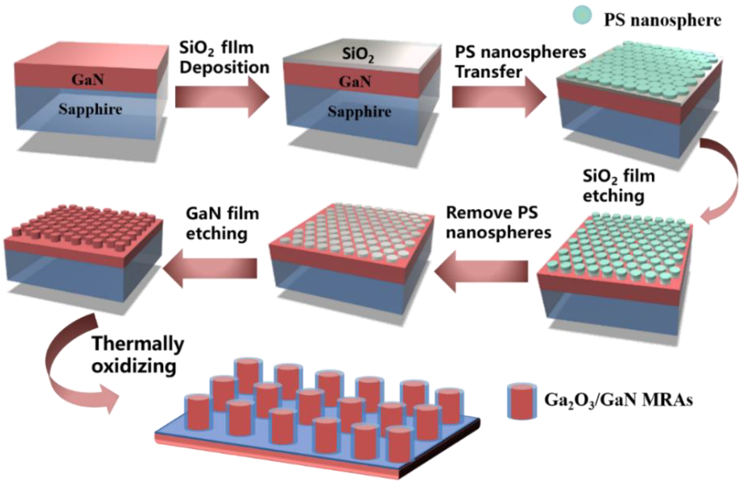
To take advantage of the internal gain brought by the special band structure of Ga2O3/GaN heterojunction, the Micro-architectonics of Ga2O3/GaN with core-shell structure were fabricated. Figure 1 is a schematic of the Ga2O3/GaN core-shell MRAs fabrication. GaN/sapphire samples with approximately 5 μm-thick unintentionally doped GaN epitaxial layer were used in this study. The GaN/sapphire wafers were ultrasonically cleaned in acetone and isopropyl alcohol for 15 min and then dipped into a diluted hydrochloric acid water solution (HCL:H2O = 1:1) for 5 min to eliminate the native oxide. A SiO2 film with a thickness of 200 nm was deposited on GaN using plasma-enhanced chemical vapor deposition (SENTECH SI500D). Subsequently, the polystyrene microsphere solution and alcohol were mixed in a 1:1 ratio, and then the polystyrene microspheres were transferred to the surface of the sample. A highly ordered self-assembled monolayer of microspheres with a diameter of 1.7 μm was arranged on the sample. To reduce the size of the microspheres and increase the distance between them, the samples were treated with oxygen plasma for 10 min. The polystyrene microsphere template was then transferred to the SiO2 film by etching the SiO2 film using inductively coupled plasma (ICP) with CF4 gas for 120 s. After the ICP etching process, the polystyrene nanospheres were eliminated by dipping the sample in tetrahydrofuran for 2 h and sonicating for 30 s. Subsequently, the SiO2 template was transferred to the GaN film through etching of the GaN film by ICP with Cl2 and BCl3 gases. Then, the sample was dipped in the BOE solution to eliminate the SiO2 mask, and GaN MRAs with a cone morphology were fabricated. Subsequently, the sample was placed in an oxidizing furnace. The heating time from room temperature to 1000 °C was approximately 55 min in an oxygen-gas environment. GaN was oxidized in a quartz tube furnace injected with 50 sccm of oxygen gas at 1000 °C for 45 min at atmospheric pressure. Finally, the samples were removed from the oxidizing furnace when the temperature was reduced to 200 °C in a nitrogen protection environment. An interdigitated metal contact (Ti/Al) with a thickness of 30/100 nm was patterned using standard photolithography (Karlsuss MA6/BA6), DC magnetron sputtering, and lift-off processes. Each device comprised 10 pairs of interdigital electrodes with lengths, widths, and spacings of 300, 6, and 6 μm, respectively. Consequently, the effective illumination area was 3.42 × 10⁻⁴ cm2. The fabricated PD was finally annealed by rapid thermal annealing under an N2 atmosphere at 200 °C for 120 s. The contrast PD based on the planar Ga2O3/GaN film was fabricated using a direct high-temperature oxidization process from a GaN film, as described above.
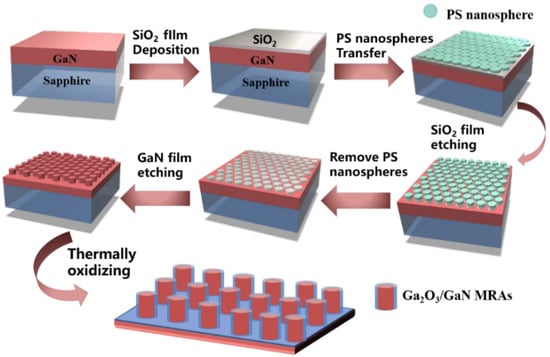
Figure 1.
Schematic of the Ga2O3/GaN MRAs fabrication.
To characterize the material properties, the surface and cross-sectional morphology, microstructure, and the elemental mapping were determined using a ZEISS SIGMA high-resolution field emission scanning electron microscope (FE-SEM). Phase formation and crystallinity were monitored using a Helios Nano-Lab 460HP high-resolution transmission electron microscope (HR-TEM). The I–V characteristics were measured using a Keithley 2410 source meter and Keithley 6514 programmable electrometer. A 450 W Xe arc lamp, mechanical chopper, and lock-in amplifier were applied to measure the photocurrent response spectra. The system was calibrated using a standard silicon detector. The devices were all illuminated perpendicularly to the front metal/semiconductor contact side. All measurements were performed at room temperature.
3. Results
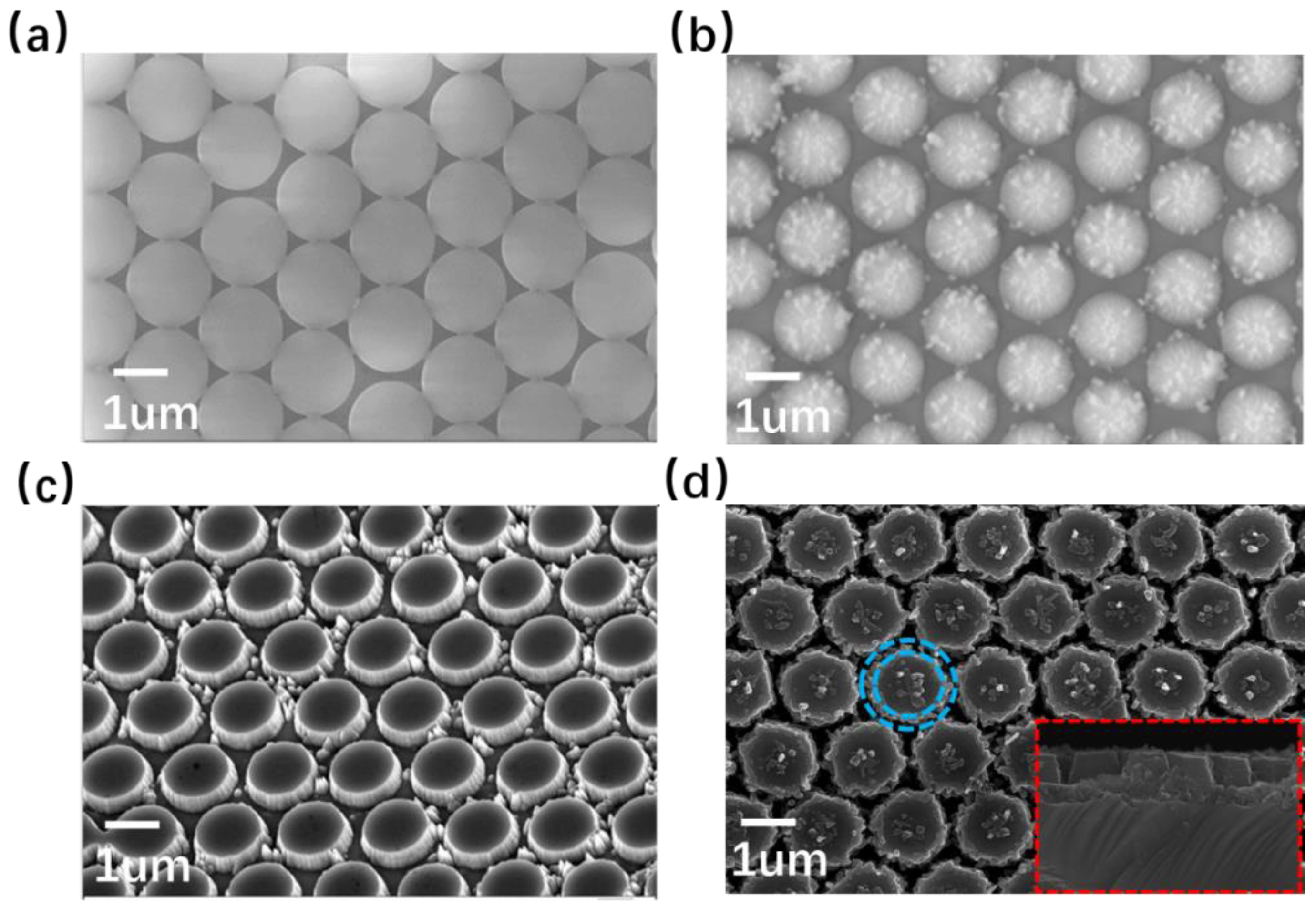
Figure 2a shows the surface morphology of the polystyrene microspheres. A highly ordered self-assembled monolayer of microspheres with a diameter of 1.7 μm was arranged on the sample. Other sizes of the polystyrene microspheres can also be used to fabricate the GaN rod arrays with different sizes. The diameter of the microspheres was reduced to 1.3 μm and the spacing of the microspheres increased after oxygen plasma treatment, as shown in Figure 2b. GaN rod arrays with different sizes and distances can also be prepared flexibly by adjusting the power and duration of oxygen plasma processing. Figure 2c shows the surface morphology of the GaN MRAs, and the highly ordered GaN MRAs with a diameter of about 1.3 μm was obtained. This size is similar to the size of the polystyrene microspheres after plasma treatment. Figure 2d shows the surface morphology of the oxidized Ga2O3/GaN MRAs. The diameter of the Ga2O3/GaN MRAs was approximately 1.35 μm. The height of the Ga2O3/GaN MRAs was approximately 750 nm, as shown in the inset of Figure 2d. Clearly, the Ga2O3/GaN MRAs show a core-shell structure, in which the outer shell is Ga2O3 with a 200–300 nm thickness and the core is GaN with an 850–1050 nm thickness. Some Ga2O3 grains with several hundred nanometers in size were observed on the top surface of the MRAs, which was also confirmed in our previous study. The X-ray diffraction (XRD) spectrum of the sample and morphology of the planar Ga2O3/GaN film were similar to those previously reported and are not shown here [54,55,59,60,61].
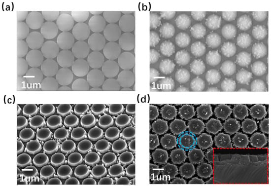
Figure 2.
(a) Surface SEM image of microspheres. (b) Surface SEM image of microsphere after oxygen plasma treatment. (c) Surface morphology of the GaN MRAs after etching the GaN film. (d) Surface morphology of the oxidized Ga2O3/GaN MRAs. The inset shows the cross-sectional SEM image of Ga2O3/GaN MRAs.
To assess the photoresponse characteristics of the planar Ga2O3/GaN film and Micro-architectonics of Ga2O3/GaN core-shell rod arrays, MSM PD based on a planar Ga2O3/GaN film (sample A) and Ga2O3/GaN MRAs (sample B) were fabricated. The device structure diagram of sample B is shown in inset of Figure 3b. The MSM structure, that is, the two electrodes constructed directly on the MRAs, had a large electrode area, which enabled the efficient collection of photogenerated carriers. Moreover, owing to the intrinsic high valence-band barrier between Ga2O3 and GaN (1.4 eV), the holes generated in GaN will be blocked at the interface of Ga2O3/GaN heterojunction underneath the electrode, resulting in a greater internal gain. The larger metal electrode area will cause more holes to be blocked at the interface of Ga2O3/GaN heterojunction, resulting in greater internal gain. The spectral response from 200 to 400 nm at applied bias of 7 V was investigated. The spectral responsivity values via wavelength are calculated using the relation [29]:
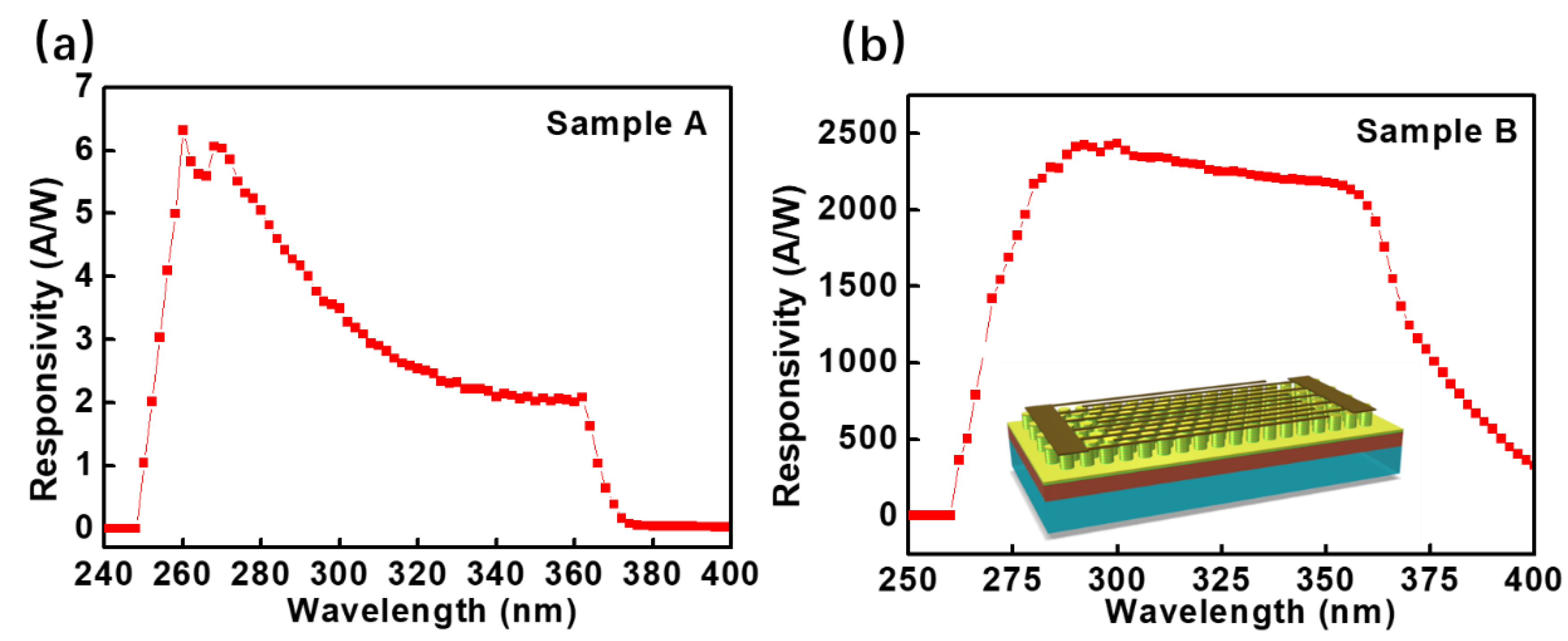
where Iph and IDark are the currents measured under illumination and dark conditions, respectively, and Pλ is the incident power density at a specific wavelength of λ, which was calibrated using a standard silicon detector. The R dependences on wavelength under the applied bias of 7 V for samples A and B are shown in Figure 3a and Figure 3b, respectively. Both PDs exhibited a wide-spectrum response in the BUV region. When the illumination wavelength exceeds 370 nm, the responsivity of sample A decreases rapidly, which corresponds to the spectral response cutoffs of GaN material. Sample B has an obvious spectral response at 370–400 nm, which is attributable to the damage of GaN crystal structure by etching process during the preparation of GaN rod arrays, forming many surface defects in GaN and inducing the defect response. Therefore, it is necessary to further optimize the preparation process in the future. As shown in Figure 3a, the peak responsivity was 6.3 A/W at 260 nm for sample A, and the responsivity at the range of 250–360 nm exceeded 2 A/W. For sample B, the peak responsivity was 2300 A/W at 280 nm, the peak responsivity is enhanced by approximately 4 × 10² times compared with sample A (6.3 A/W), and the responsivity at the 270–360 nm band exceeded 1500 A/W, as shown in Figure 3b. It is also superior to some reported values [34,35]. Both of the two samples have high responsivity, indicating that the two PDs have a large external quantum efficiency (EQE), which is defined as the number of electrons generated per incident photon and can be obtained using the following equation [27]:
where R, h, c, q, and λ are the responsivity, Planck’s constant, speed of light, electron charge, and wavelength of the incident optical light, respectively. It is observed that sample A exhibited an EQE of approximately 3 × 10³% for 260 nm and sample B exhibited an ultrahigh EQE of approximately 1.02 × 10⁶% for 280 nm. Compared with sample A, the internal gain of sample B is significantly increased. Obviously, it cannot be explained by the increase in light absorption efficiency owing to the large surface area of MRAs. This is assignable to the larger surface area of the MRA coupled with the Ga2O3/GaN heterostructure. This is discussed in detail later in this study.
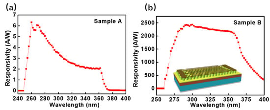
Figure 3.
(a) Spectral responsivity values of sample A as a function of wavelength at 7 V bias, (b) spectral responsivity values of sample B as a function of wavelength at 7 V bias. The inset shows the device diagram of sample B.
Detectivity (D*), which usually describes the smallest detectable signal, is another key figure of merit of PDs. The detectivity (D*) can be expressed as [27]
where S (3.42 × 10⁻⁴ cm2) is the effective area under illumination with the shot noise from IDark regarded as the major component of the total noise. The detectivity D* of sample A was calculated as 4.47 × 10¹² Jones for 260 nm. The detectivity D* of sample B was calculated as 2.65 × 10¹³ Jones for 280 nm and shows that the ability to detect weak signals is improved.
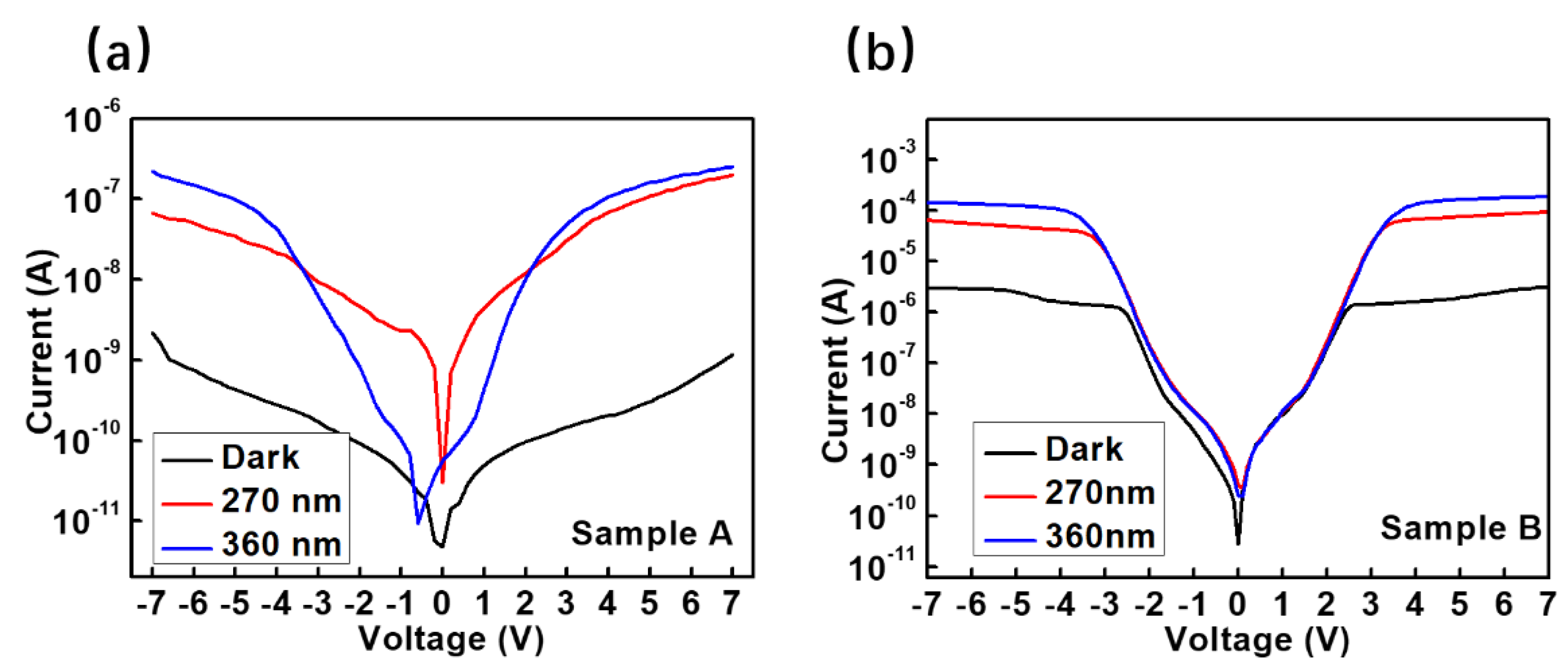
Figure 4a,b shows the I–V characteristics of samples A and B under dark conditions and the illumination of 270 nm/360 nm light, respectively. For sample A, the dark current at 7 V bias is 1.14 × 10⁻⁹ A, and the photocurrents are 1.99 × 10⁻⁷ and 2.44 × 10⁻⁷ A at 270 nm and 360 nm light illuminations, respectively, while the photo-to-dark ratios for 360 nm and 270 nm/dark current both exceeded 102. Such low light-to-dark ratio is mainly due to the rather weak intensity of the 270 nm and 360 nm light illuminations, which is separated from the xenon lamp light passing through the monochromator. When the bias voltage is in the range of −3~3 V, the photocurrent at 360 nm light illumination is less than that at 270 nm light illumination, indicating that the depletion region is mainly in the Ga2O3 layer. As the bias voltage increases, the photocurrent for 360 nm increases rapidly, and exceeds the photocurrent for 270 nm, which indicates that the depletion layer of the device enters the GaN layer. The PD presents B-UV detection, which is consistent with the results of the response spectrum. For sample B, the dark current at 7 V bias is up to 10−6 A, which is three orders of magnitude higher than that of sample A. The significant increase in dark current is attributable to the following reasons. The larger electrode area of sample B not only increased the photocurrent, but also inevitably led to larger dark current. Meanwhile, the etching process of the GaN film also caused a deterioration of the GaN crystalline quality, resulting in a greater current leakage. Therefore, the photocurrent was evidently higher than that of dark current until the bias voltage exceeding 3.2 V. The photo-to-dark ratios for 360 nm and 270 nm/dark currents both exceeded 10. It is necessary to further optimize the process to improve the light/dark ratio.
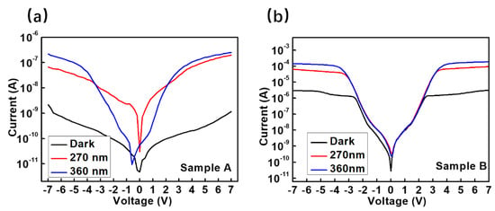
Figure 4.
I−V characteristics of samples A (a) and B (b) in the dark and under 254 nm/365 nm UV illuminations.
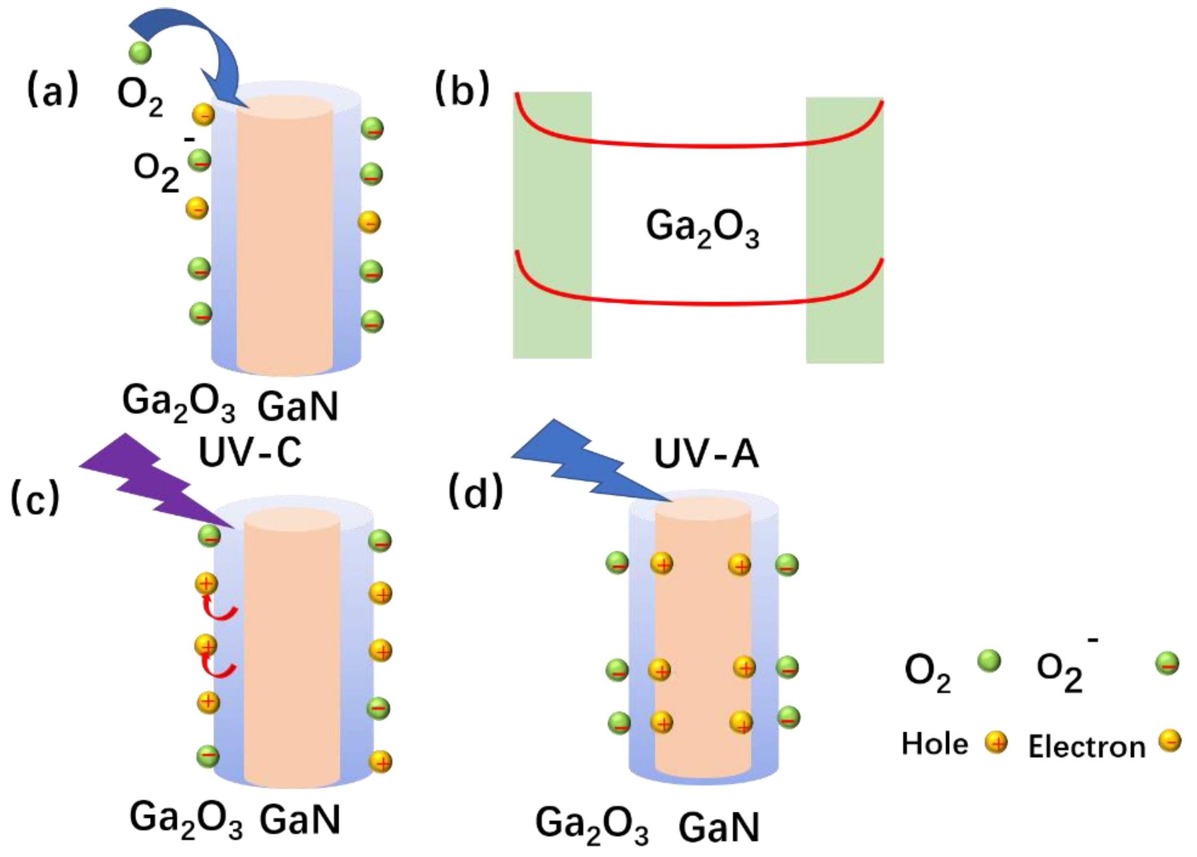
To clearly explain the increased internal gain in sample B, the photodetection model and mechanism of sample B are schematically shown in Figure 5. As shown in Figure 5a,b, the microarchitectonics of Ga2O3/GaN core-shell rod arrays have a larger surface area, and more ambient oxygen molecules are adsorbed on the surface of the MRAs in the dark environment. The free electrons on the surface of the Ga2O3 film were trapped by oxygen molecules, forming a depletion layer and the energy band bending near the surface of the MRAs. When the device was illuminated under UV-C light, the photogenerated holes in Ga2O3 migrated to the surface of Ga2O3 due to the bending band. Compared with the photogenerated electrons in Ga2O3, the photogenerated holes in Ga2O3 that migrate to the surface of Ga2O3, were difficult to collect by the electrode, resulting in a large gain. When the device was illuminated under UV-A light, because negatively charged oxygen ions existed on the surface of the Ga2O3 film after the reaction with O2, the photogenerated holes in the GaN film were aggregated at the interface of Ga2O3/GaN owing to the capacitance effect. These holes were also difficult for the electrode to collect, resulting in an enhanced gain. Therefore, sample B exhibited a greater internal gain than sample A in BUV band range.
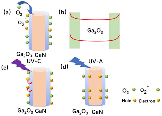
Figure 5.
(a,b) Schematic of reaction of Ga2O3/GaN core-shell micron rod with oxygen and band of Ga2O3 films after reaction with oxygen respectively (c) Schematic of holes transferred to the surface of Ga2O3 film under UV-C illumination; (d) Schematic of photo-generated holes in GaN layer gathering at Ga2O3/GaN heterojunction interface owing to capacitance effect under UV-A illumination.
Moreover, the Ga2O3/GaN core-shell MRAs with higher surface-to-volume ratios effectively improved the light absorption efficiency and thus excited more photogenerated carriers. Because of the larger electrode area, these additional photogenerated electrons can be effectively collected and increase the photocurrent. In addition, more holes were blocked at the Ga2O3/GaN interface underneath the electrode, resulting in high responsivity. Since the Ga2O3/GaN heterojunction has the low conduction band barrier (0.1 eV) and high valence band barrier (1.4 eV), the photogenerated electrons in the GaN layer can pass through the Ga2O3/GaN heterojunction and be collected by the electrode. Meanwhile, the photogenerated holes in GaN are effectively blocked in the Ga2O3/GaN heterojunction, noting that these blocked photogenerated holes are mainly located at the Ga2O3/GaN heterojunction interface below the electrode. A larger metal electrode area can block more holes, thus leading to greater photoconductance gain. The designed structure effectively coupled the optical field enhancement effect with the internal gain of the heterojunction, resulting in ultra-high responsivity of the PDs.
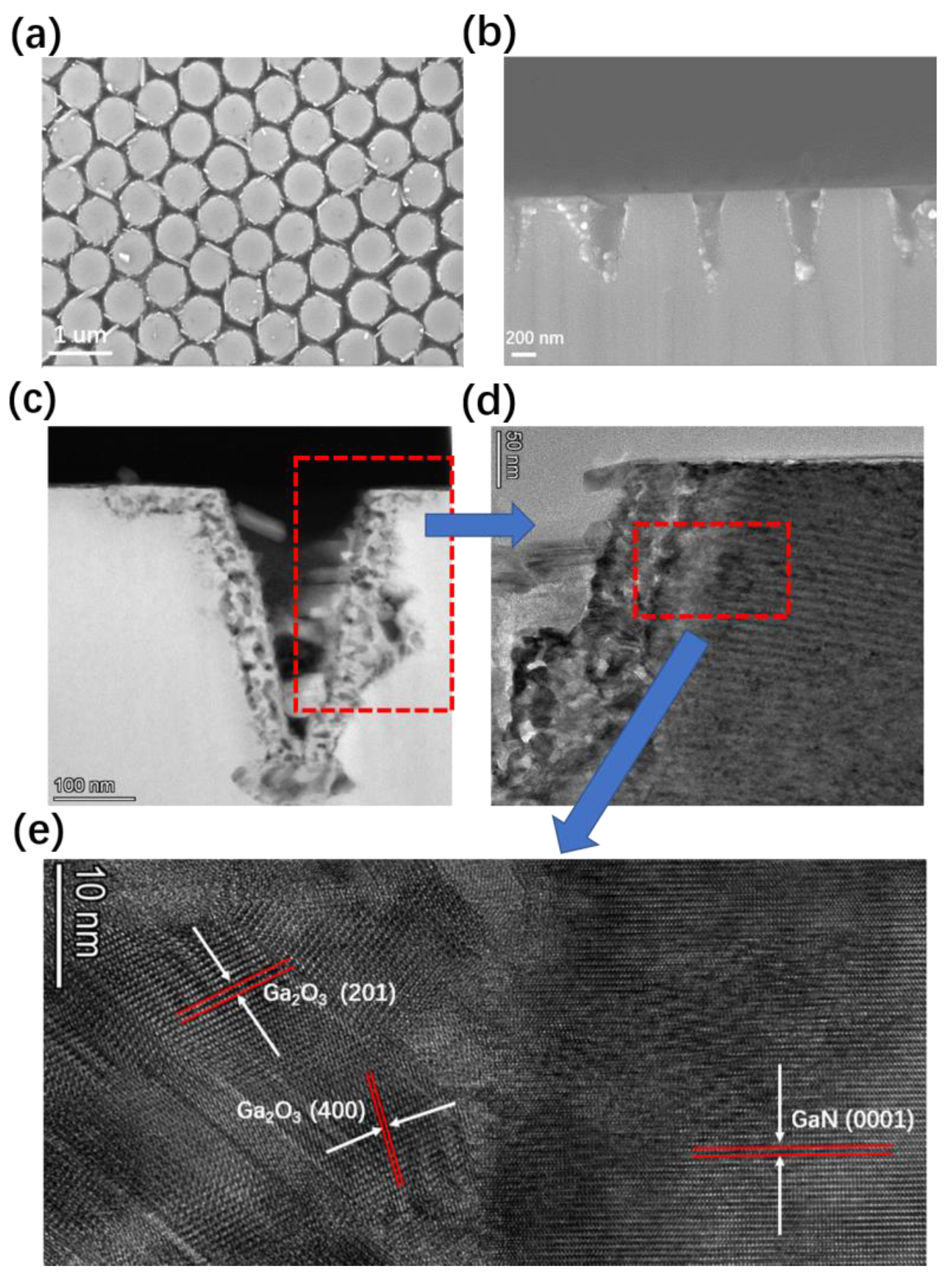
Whether the increased gain caused by the oxygen adsorption, or the large electrode area coupled by the internal gain of the Ga2O3/GaN heterojunction, both are related to the surface area of Ga2O3/GaN core-shell rod arrays. To further confirm the above mechanism, Ga2O3/GaN NRAs with larger surface areas were fabricated using the same method as described above, except that the polystyrene microspheres with a diameter of 1 μm was applied as the mask template and the thermal oxidation time was reduced to 30 min. Figure 6a,b shows the surface and cross-sectional topography of the NRAs. As shown in Figure 6a,b, the highly ordered Ga2O3/GaN NRAs were obtained, the diameter of the nano-column is approximately 700 nm and the height is approximately 400–450 nm. A thin layer of Ga2O3 was identified in the outermost layer of the NRA. In order to demonstrate the formation of the Ga2O3/GaN core-shell structures, high-resolution HR-TEM inspections were performed. As shown in Figure 6c–e, the outmost shell with a thickness of 10–50 nm is confirmed, which corresponds to the β-Ga2O3 (201) and β-Ga2O3 (400), and the core area corresponds to GaN (0001). These results indicate that the GaN NRAs were oxidized at high temperature and form the polycrystalline Ga2O3 film on the GaN surface.

Figure 6.
(a) Surface morphology of the oxidized Ga2O3/GaN NRAs. (b) Cross-section SEM image of Ga2O3/GaN NRAs. (c,d) Low-magnification TEM image of the core-shell NRA. (e) HR-TEM image of the core-shell NRA.
To further confirm the formation of the nanoarchitectonics of Ga2O3/GaN rod arrays with core-shell structure by thermal oxidation, energy dispersive X-ray (EDX) and element mapping characterizations were performed on the cross section of Ga2O3/GaN NRAs. As shown in Figure 7a–e, it can be intuitively seen that Ga and O elements are mainly distributed in the outermost layer of the nanorods, which represents the formed Ga2O3 thin film layer. The Ga and N elements are mainly distributed inside the nanorods, which corresponds to the GaN layer inside. These results further demonstrate the formation of the Ga2O3/GaN core-shell structures. To assess the photoresponse characteristics of the nano-architectonics of Ga2O3/GaN core-shell rod arrays, the PD (sample C) was fabricated in these structures with identical preparation method. Figure 8 shows the responsivity spectrum of sample C. The PDs exhibited a wide-spectrum response in the BUV region. An obvious optical response at 370–400 nm is observed in sample C, which is the same as sample B, indicating the existence of interband response. The peak responsivity of sample C is in the UV-A band range, while the case for sample B is in the UV-C band as described above. This is mainly because the thickness of Ga2O3 in sample C is ultrathin, only 10–50 nm, and the sample C mainly exhibits UV-A band response induced from GaN material. As shown in Figure 8, the peak responsivity was 2.65 × 10⁴ A/W for 365 nm at 7 V applied bias, and the responsivity at the 270–360 nm band exceeded 1.5 × 10⁴ A/W, which is a further order of magnitude enhancement than sample B. These results show that larger surface area leads to greater internal gain, which is consistent with the proposed mechanisms as aforementioned. Nevertheless, it is possible to further optimize the thickness of Ga2O3 film on GaN by adjusting the oxidation time, and realize the tunable detection in UV band. Overall, we proposed a simple method to fabricate the B-UV PD with high responsivity, which enables the detection under weak light illuminations.
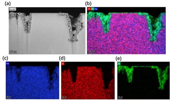
Figure 7.
(a) Cross-section SEM image of Ga2O3/GaN NRA and (b) corresponding element mapping; (c–e) are distribution diagrams of Ga, N and O elements respectively.
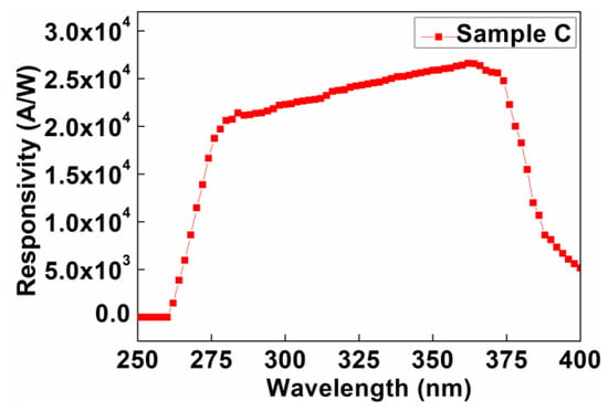
Figure 8.
Spectral responsivity values of sample C as a function of wavelength at 7 V bias.
4. Conclusions
In this study, we designed and demonstrated a BUV PD based on Ga2O3/GaN core-shell MRAs and NRAs, which were fabricated using partially thermally oxidizing GaN MRAs and NRAs. The PD based on MRAs showed an ultrahigh responsivity of 2300 A/W for 280 nm and over 1500 A/W for the 270–360 nm band at 7 V. The detectivity and external quantum efficiency were approximately 2.65 × 10¹³ Jones and 1.02 × 10⁶% at 280 nm, respectively. The responsivity was further increased to 2.65 × 10⁴ A/W for 280 nm and over 1.5 × 10⁴ A/W for 270–360 nm using the nanorod arrays. Such high performance can be attributed to the blocking of photo-generated holes. Specifically, the large surface area of Ga2O3/GaN MRAs and NRAs led to the migration of photogenerated holes to the surface of Ga2O3 film, which was caused by the band bending of Ga2O3 surface induced by oxygen absorption mechanism and resulted in the large internal gains. Moreover, the larger metal electrode area can block more holes at the heterojunction interface of Ga2O3/GaN, which was caused by the larger valence-band barrier (1.4 eV). Overall, the proposed metal–semiconductor–metal structure enables a large surface area and is suitable for mass production.
Author Contributions
R.T., J.L. and K.H. conceived the idea and designed the experiments. J.L. and K.H. supervised the project. R.T., G.L. and N.G. explored the oxidation process and the devices’ fabrication. R.T., G.L. and J.L. performed the device characterization and the simulation. R.T., X.H., J.L., K.H., J.K. and R.Z. analyzed the data and contributed to the mechanism investigation. R.T., J.L. and K.H. wrote the manuscript. All authors participated in the discussion and commented on the manuscript. All authors have read and agreed to the published version of the manuscript.
Funding
This research was funded by Key Technologies Research and Development Program (2021YFB3600101); National Natural Science Foundation of China (62174141, 61974126, 51902273, and 61874090); Key scientific and technological Program of Xiamen (3502Z20191016); Natural Science Foundation of Fujian Province (No. 2021J01008).
Conflicts of Interest
The authors declare no conflict of interest. The funders had no role in the design of the study; in the collection, analyses, or interpretation of data; in the writing of the manuscript; or in the decision to publish the results.
References
- Aslam, S.; Miko, L.; Stahle, C.; Franz, D.; Pugel, D.; Guan, B.; Zhang, J.; Gaska, R. Dual-band deep ultraviolet AlGaN photodetectors. Electron. Lett. 2007, 43, 1382–1384. [Google Scholar] [CrossRef]
- Assefa, S.; Xia, F.; Vlasov, Y.A. Reinventing germanium avalanche photodetector for nanophotonic on-chip optical interconnects. Nature 2010, 464, 80–84. [Google Scholar] [CrossRef] [PubMed]
- Gong, X.; Tong, M.; Xia, Y.; Cai, W.; Moon, J.S.; Cao, Y.; Yu, G.; Shieh, C.-L.; Nilsson, B.; Heeger, A.J. High-Detectivity Polymer Photodetectors with Spectral Response from 300 nm to 1450 nm. Science 2009, 325, 1665–1667. [Google Scholar] [CrossRef] [PubMed]
- Konstantatos, G.; Sargent, E.H. Nanostructured materials for photon detection. Nat. Nanotechnol. 2010, 5, 391–400. [Google Scholar] [CrossRef] [PubMed]
- Monroy, E.; Omn, F.; Calle, F. Wide-Bandgap Semiconductor Ultraviolet Photodetectors. Semicond. Sci. Technol. 2003, 18, R33–R51. [Google Scholar] [CrossRef]
- Zheng, W.; Lin, R.; Zhang, D.; Jia, L.; Ji, X.; Huang, F. A new superconductor of cuprates with unique features. Adv. Opt. Mater. 2018, 6, 1800697. [Google Scholar] [CrossRef]
- Li, J.Z.; Lin, J.Y.; Jiang, H.X.; Khan, M.A. Effects of persistent photoconductivity on the characteristic performance of an AlGaN/GaN heterostructure ultraviolet detector. Appl. Phys. Lett. 1998, 72, 2868–2870. [Google Scholar] [CrossRef]
- Ji, L.W.; Peng, S.M.; Su, Y.K.; Young, S.-J.; Wu, C.Z.; Cheng, W.B. Ultraviolet photodetectors based on selectively grown ZnO nanorod arrays. Appl. Phys. Lett. 2009, 94, 203106. [Google Scholar] [CrossRef]
- Lupan, O.T.; Braniste, M.; Deng, L.; Ghimpu, I.; Paulowicz, Y.K.; Mishra, L.; Kienle, R.; Adelung, I.; Tiginyanu, I. Rapid switching and ultra-responsive nanosensors based on individual shell–core Ga2O3/GaN:Ox@SnO2 nanobelt with nanocrystalline shell in mixed phases. Sens. Actuators B 2015, 221, 544–555. [Google Scholar] [CrossRef]
- Yu, J.; Shan, C.X.; Huang, X.M.; Zhang, X.W.; Wang, S.P.; Shen, D.Z. ZnO-based ultraviolet avalanche photodetectors. J. Phys. D Appl. Phys. 2013, 46, 305105. [Google Scholar] [CrossRef]
- Yu, J.; Shan, C.X.; Liu, J.S.; Zhang, X.W.; Li, B.H.; Shen, D.Z. MgZnO avalanche photodetectors realized in Schottky structures. Phys. Status Solidi. RRL—Rapid Res. Lett. 2013, 7, 425–428. [Google Scholar] [CrossRef]
- Shao, Z.G.; Chen, D.J.; Lu, H.; Zhang, R.; Cao, D.P.; Luo, W.J.; Zheng, Y.D.; Li, L.; Li, Z.H. High-Gain AlGaN Solar-Blind Avalanche Photodiodes. IEEE Electron Device Lett. 2014, 35, 372–374. [Google Scholar] [CrossRef]
- Huang, Y.; Chen, D.J.; Lu, H.; Dong, K.X.; Zhang, R.; Zheng, Y.D.; Li, L.; Li, Z.H. Back-illuminated separate absorption and multiplication AlGaN solar-blind avalanche photodiodes. Appl. Phys. Lett. 2012, 101, 253516. [Google Scholar] [CrossRef]
- Tut, T.; Gokkavas, M.; Inal, A.; Ozbay, E. AlxGa1-xN-based avalanche photodiodes with high reproducible avalanche gain. Appl. Phys. Lett. 2007, 90, 163506. [Google Scholar] [CrossRef]
- Huang, Z.; Li, J.; Zhang, W.; Jiang, H. AlGaN Solar-Blind Avalanche Photodiodes with Enhanced Multiplication Gain Using Back-Illuminated Structure. Appl. Phys. Express 2013, 6, 054101. [Google Scholar] [CrossRef]
- Tut, T.; Gokkavas, M.; Butun, B.; Butun, S.; Ulker, E.; Ozbay, E. Experimental evaluation of impact ionization coefficients in AlxGa1−xN based avalanche photodiodes. Appl. Phys. Lett. 2006, 89, 183524. [Google Scholar] [CrossRef]
- Xie, X.H.; Zhang, Z.Z.; Shan, C.X.; Chen, H.Y.; Shen, D.Z. Dual-color ultraviolet photodetector based on mixed-phase-MgZnO/i-MgO/p-Si double heterojunction. Appl. Phys. Lett 2012, 101, 081104. [Google Scholar] [CrossRef]
- Xuan, H.C.; Wen, X.M.; Yang, X.; Bo, F.; Zhi, T.J.; Jian, D.Y. Highly Narrow-Band Polarization-Sensitive Solar-Blind Photodetectors Based on β-Ga2O3 Single Crystals. ACS Appl. Mater. Interfaces 2019, 11, 7131–7137. [Google Scholar]
- Kong, W.Y.; Wu, G.A.; Wang, K.Y.; Zhang, T.F.; Zou, Y.F.; Wang, D.D.; Luo, L.B. Graphene-β-Ga2O3 Heterojunction for Highly Sensitive Deep UV Photodetector Application. Adv. Mater. 2016, 28, 10725–10731. [Google Scholar] [CrossRef]
- Pratiyush, A.; Krishnamoorthy, S.; Solanke, S.S.; Xia, V.Z.; Muralidharan, R.; Rajan, S.; Nath, D.N. High responsivity in molecular beam epitaxy grown β-Ga2O3 metal semiconductor metal solar blind deep-UV photodetector. Appl. Phys. Lett. 2017, 110, 221107. [Google Scholar] [CrossRef]
- Qu, Y.; Wu, Z.; Ai, M.; Guo, D.; An, Y.; Yang, H.; Li, L.; Tang, W. Enhanced Ga2O3/SiC ultraviolet photodetector with graphene top electrodes. J. Alloys Compd 2016, 680, 247–251. [Google Scholar] [CrossRef]
- Zhao, B.; Wang, F.; Chen, H.; Zheng, L.; Su, L.; Zhao, D.; Fang, X. An Ultrahigh Responsivity (9.7 mA W− ( ) Self-Powered Solar-Blind Photodetector Based on Individual ZnO-Ga2O3 Heterostructures. Adv. Funct. Mater. 2017, 27, 1700264. [Google Scholar] [CrossRef]
- Guo, D.Y.; Liu, H.; Li, P.; Wu, Z.; Wang, S.; Cui, C.; Li, C.; Tang, W. Zero-Power-Consumption Solar-Blind Photodetector Based on β-Ga2O3/NSTO Heterojunction. ACS Appl. Mater. Interfaces 2017, 9, 1619–1628. [Google Scholar] [CrossRef] [PubMed]
- Chen, X.; Liu, K.; Zhang, Z.; Wang, C.; Li, B.; Zhao, H.; Zhao, D.; Shen, D. Self-Powered Solar-Blind Photodetector with Fast Response Based on Au/β-Ga2O3 Nanowires Array Film Schottky Junction. ACS Appl. Mater. Interfaces 2016, 8, 4185–4191. [Google Scholar] [CrossRef]
- Li, P.; Shi, H.; Chen, K.; Guo, D.; Cui, W.; Zhi, Y.; Wang, S.; Wu, Z.; Chen, Z.; Tang, W. Construction of GaN/Ga2O3 p–n junction for an extremely high responsivity self-powered UV photodetector. J. Mater. Chem. C 2017, 5, 10562–10570. [Google Scholar] [CrossRef]
- Kanika, A.; Neeraj, G.; Mahesh, K.; Mukesh, K. Ultra-high-performance of Self-Powered β-Ga2O3 Thin Film Solar-blind Photodetector Grown on Cost-Effective Si Substrate using High-Temperature Seed Layer. ACS Photonics 2018, 5, 2391–2401. [Google Scholar]
- Qian, L.-X.; Wu, Z.-H.; Zhang, Y.-Y.; Lai, P.T.; Liu, X.-Z.; Li, Y.-R. Ultrahigh-Responsivity, Rapid-Recovery, Solar-Blind Photodetector Based on Highly Nonstoichiometric Amorphous Gallium Oxide. ACS Photon. 2017, 4, 2203–2211. [Google Scholar] [CrossRef]
- Weng, W.Y.; Hsueh, T.J.; Chang, S.J.; Huang, G.J. A β-Ga2O3/GaN Hetero-Structured Solar-Blind and Visible-Blind Dual-Band Photodetector. IEEE Sens. J. 2011, 11, 5. [Google Scholar] [CrossRef]
- Guo, D.; Su, Y.; Shi, H.; Li, P.; Zhao, N.; Ye, J.; Wang, S.; Liu, A.; Chen, Z.; Li, C.; et al. Self-Powered Ultraviolet Photodetector with Superhigh Photoresponsivity (3.05 A/W) Based on the GaN/Sn:β-Ga2O3 pn Junction. ACS Nano 2018, 12, 12827–12835. [Google Scholar] [CrossRef]
- Lin, W.; Zheng, D.; Zhang, Z.; Zhang, Q.; Liao, L.; Yang, F.; Huang, F. High-Performance Graphene/β-Ga2O3 Heterojunction Deep-Ultraviolet Photodetector with Hot-Electron Excited Carrier Multiplication. ACS Appl. Mater. Interfaces 2018, 10, 22419–22426. [Google Scholar] [CrossRef]
- Kalra, A.; Vura, S.; Rathkanthiwar, S.; Muralidharan, R.; Raghavan, S.; Nath, D.N. Demonstration of High-Responsivity Epitaxial β-Ga2O3/GaN Metal–Heterojunction-Metal Broadband UV-A/UV-C Detector. Appl. Phys. Express 2018, 11, 064101. [Google Scholar] [CrossRef]
- Nakagomi, S.; Sato, T.; Takahashi, Y.; Kokubun, Y. Deep Ultraviolet Photodiodes Based on the β-Ga2O3/GaN Heterojunction. Sens. Actuators A Phys. 2015, 232, 208–213. [Google Scholar] [CrossRef]
- Zeng, C.H.; Ma, Y.J.; Zhang, B.S.; Xu, Y.M.; Kong, M. Broadband Ultraviolet Photodetector Based on Graphene/β-Ga2O3/GaN Heterojunction. Mater. Sci. Forum 2020, 1014, 131–136. [Google Scholar] [CrossRef]
- He, T.; Zhang, X.; Ding, X.; Sun, C.; Zhao, Y.; Yu, Q.; Ning, J.; Wang, R.; Yu, G.; Lu, S.; et al. Broadband Ultraviolet Photodetector Based on Vertical Ga2O3/GaN Nanowire Array with High Responsivity. Adv. Opt. Mater. 2019, 7, 1801563. [Google Scholar] [CrossRef]
- Wang, S.; Chen, K.; Zhao, H.; He, C.; Wu, C.; Guo, D.; Zhao, N.; Ungar, G.; Shen, J.; Chu, X.; et al. β-Ga2O3 Nanorod Arrays with High Light-to-Electron Conversion for Solar-Blind Deep Ultraviolet Photodetection. RSC Adv. 2019, 9, 6064–6069. [Google Scholar] [CrossRef] [PubMed]
- Kalarickal, N.K.; Xia, Z.; McGlone, J.; Krishnamoorthy, S.; Moore, W.; Brenner, M.; Arehart, A.R.; Ringel, S.A.; Rajan, S. Mechanism of Si Doping in Plasma Assisted MBE Growth of β-Ga2O3. Appl. Phys. Lett. 2019, 115, 152106. [Google Scholar] [CrossRef]
- Pratiyush, A.S.; Krishnamoorthy, S.; Kumar, S.; Xia, Z.; Muralidharan, R.; Rajan, S.; Nath, D.N. Demonstration of Zero Bias Responsivity in MBE Grown β-Ga2O3 Lateral Deep-UV Photodetector. Jpn. J. Appl. Phys. 2018, 57, 060313. [Google Scholar] [CrossRef]
- Sasaki, K.; Higashiwaki, M.; Kuramata, A.; Masui, T.; Yamakoshi, S. MBE grown Ga2O3 and its power device applications. J. Cryst. Growth 2013, 378, 591–595. [Google Scholar] [CrossRef]
- Sasaki, K.; Higashiwaki, M.; Kuramata, A.; Masui, T.; Yamakoshi, S. Growth temperature dependences of structural and electrical properties of Ga2O3 epitaxial films grown on β-Ga2O3 (010) substrates by molecular beam epitaxy. J. Cryst. Growth 2014, 392, 30–33. [Google Scholar] [CrossRef]
- Alema, F.; Hertog, B.; Mukhopadhyay, P.; Zhang, Y.; Mauze, A.; Osinsky, A.; Schoenfeld, W.V.; Speck, J.S.; Vogt, T. Solar Blind Schottky Photodiode Based on an MOCVD-Grown Homoepitaxial β-Ga2O3 Thin Film. APL Mater. 2019, 7, 022527. [Google Scholar] [CrossRef]
- Feng, Z.; Anhar Uddin Bhuiyan, A.F.M.; Karim, M.R.; Zhao, H. MOCVD Homoepitaxy of Si-Doped (010) β-Ga2O3 Thin Films with Superior Transport Properties. Appl. Phys. Lett. 2019, 114, 250601. [Google Scholar] [CrossRef]
- Seryogin, G.; Alema, F.; Valente, N.; Fu, H.; Steinbrunner, E.; Neal, A.T.; Mou, S.; Fine, A.; Osinsky, A. MOCVD Growth of High Purity Ga2O3 Epitaxial Films Using Trimethylgallium Precursor. Appl. Phys. Lett. 2020, 117, 262101. [Google Scholar] [CrossRef]
- Kneiß, M.; Hassa, A.; Splith, D.; Sturm, C.; von Wenckstern, H.; Schultz, T.; Koch, N.; Lorenz, M.; Grundmann, M. Tin-Assisted Heteroepitaxial PLD-Growth of κ-Ga2O3 Thin Films with High Crystalline Quality. APL Mater. 2019, 7, 022516. [Google Scholar] [CrossRef]
- Wang, Q.; Chen, J.; Huang, P.; Li, M.; Lu, Y.; Homewood, K.P.; Chang, G.; Chen, H.; He, Y. Influence of growth temperature on the characteristics of β-Ga2O3 epitaxial films and related solar-blind photodetectors. Appl. Surf. Sci. 2019, 489, 101–109. [Google Scholar] [CrossRef]
- Xu, C.; Liu, H.; Pan, X.; Ye, Z. Growth and characterization of Si-doped β-Ga2O3 films by pulsed laser deposition. Opt. Mater. 2020, 108, 110145. [Google Scholar] [CrossRef]
- Altuntas, H.; Donmez, I.; Ozgit-Akgun, C.; Biyikli, N. Electrical characteristics of β-Ga2O3 thin films grown by PEALD. J. Alloys Compd. 2014, 593, 190–195. [Google Scholar] [CrossRef]
- Choi, D.-W.; Chung, K.-B.; Park, J.-S. Low temperature Ga2O3 atomic layer deposition using gallium tri-isopropoxide and water. Thin Solid Film. 2013, 546, 31–34. [Google Scholar] [CrossRef]
- Comstock, D.J.; Elam, J.W. Atomic Layer Deposition of Ga2O3 Films Using Trimethylgallium and Ozone. Chem. Mater. 2012, 24, 4011–4018. [Google Scholar] [CrossRef]
- Zhou, H.; Alghamdi, S.; Si, M.; Qiu, G.; Ye, P.D. Al2O3/β-Ga2O3(-201) Interface Improvement Through Piranha Pretreatment and Postdeposition Annealing. IEEE Electron Device Lett. 2016, 37, 1411–1414. [Google Scholar] [CrossRef]
- Choi, J.-H.; Ham, M.-H.; Lee, W.; Myoung, J.-M. Fabrication and characterization of GaN/amorphous Ga2O3 nanocables through thermal oxidation. Solid State Commun. 2007, 142, 437–440. [Google Scholar] [CrossRef]
- Filippo, E.; Siciliano, M.; Genga, A.; Micocci, G.; Tepore, A.; Siciliano, T. Single crystalline β-Ga2O3 nanowires synthesized by thermal oxidation of GaSe layer. Mater. Res. Bull. 2013, 48, 1741–1744. [Google Scholar] [CrossRef]
- Lin, L.; Luo, Y.; Lai, P.; Lau, K.M. Influence of oxidation and annealing temperatures on quality of Ga2O3 film grown on GaN. Thin Solid Films 2006, 515, 2111–2115. [Google Scholar] [CrossRef]
- Oshima, T.; Kaminaga, K.; Mukai, A.; Sasaki, K.; Masui, T.; Kuramata, A.; Yamakoshi, S.; Fujita, S.; Ohtomo, A. Formation of Semi-Insulating Layers on Semiconducting β-Ga2O3 Single Crystals by Thermal Oxidation. Jpn. J. Appl. Phys. 2013, 52, 051101. [Google Scholar] [CrossRef]
- Tang, R.; Li, G.; Li, C.; Li, J.; Zhang, Y.; Huang, K.; Ye, J.; Li, C.; Kang, J.; Zhang, R.; et al. Localized Surface Plasmon Enhanced Ga2O3 Solar Blind Photodetectors. Opt. Express OE 2020, 28, 5731–5740. [Google Scholar] [CrossRef] [PubMed]
- Tang, R.F.; Li, G.Q.; Jiang, Y.; Gao, N.; Li, J.C.; Li, C.; Huang, K.; Kang, J.Y.; Wang, T.; Zhang, R. Ga2O3/GaN heterostructural ultraviolet photodetectors with exciton-dominated ultranarrow response. ACS Appl. Electron. Mater. 2021, 4, 188–196. [Google Scholar] [CrossRef]
- Wang, S.; Li, Y.W.; Xiu, X.Q.; Zhang, L.Y.; Hua, X.M.; Xie, Z.L.; Tao, T.; Liu, B.; Chen, P.; Zhang, R. Synthesis and characterization of β-Ga2O3@ GaN nanowires. Chin. Phys. B 2019, 28, 028104. [Google Scholar] [CrossRef]
- Zhang, L.Y.; Li, Y.W.; Xiu, X.Q.; Xin, G.Q.; Xie, Z.L.; Tao, T.; Liu, B.; Chen, P.; Zhang, R.; Zheng, Y.D. Preparation of vertically aligned GaN@Ga2O3 core-shell heterostructured nanowire arrays and their photocatalytic activity for degradation of Rhodamine B. Superlattices Microstruct. 2020, 143, 106556. [Google Scholar] [CrossRef]
- Ariga, K. Nanoarchitectonics: What’s coming next after nanotechnology? Nanoscale Horiz. 2021, 6, 364–378. [Google Scholar] [CrossRef]
- Sudhir, G.S.; Peyrot, Y.; Krüger, J.; Kim, Y.; Klockenbrink, R.; Kisielowski, C.; Rubin, M.D.; Weber, E.R.; Kriegseis, W.; Meyer, B.K. Effect of Mg, Zn, Si, and O on the Lattice Constant of Gallium Nitride Thin Films. MRS Online Proc. Libr. 1997, 482, 569–574. [Google Scholar] [CrossRef]
- Greco, G.; Fiorenza, P.; Giannazzo, F.; Alberti, A.; Roccaforte, F. Nanoscale electrical and structural modification induced by rapid thermal oxidation of AlGaN/GaN heterostructures. Nanotechnology 2013, 25, 025201. [Google Scholar] [CrossRef]
- Hayes, J.M.; Kuball, M.; Bell, A.T.; Harrison, I.; Korakakis, D.; Foxon, C.T. High-temperature processing of GaN: The influence of the annealing ambient on strain in GaN. Appl. Phys. Lett. 1999, 75, 2097–2099. [Google Scholar] [CrossRef]
Disclaimer/Publisher’s Note: The statements, opinions and data contained in all publications are solely those of the individual author(s) and contributor(s) and not of MDPI and/or the editor(s). MDPI and/or the editor(s) disclaim responsibility for any injury to people or property resulting from any ideas, methods, instructions or products referred to in the content. |
© 2023 by the authors. Licensee MDPI, Basel, Switzerland. This article is an open access article distributed under the terms and conditions of the Creative Commons Attribution (CC BY) license (https://creativecommons.org/licenses/by/4.0/).

