
A Review of Homoepitaxy of III-Nitride Semiconductors by Metal Organic Chemical Vapor Deposition and the Effects on Vertical Devices

Abstract
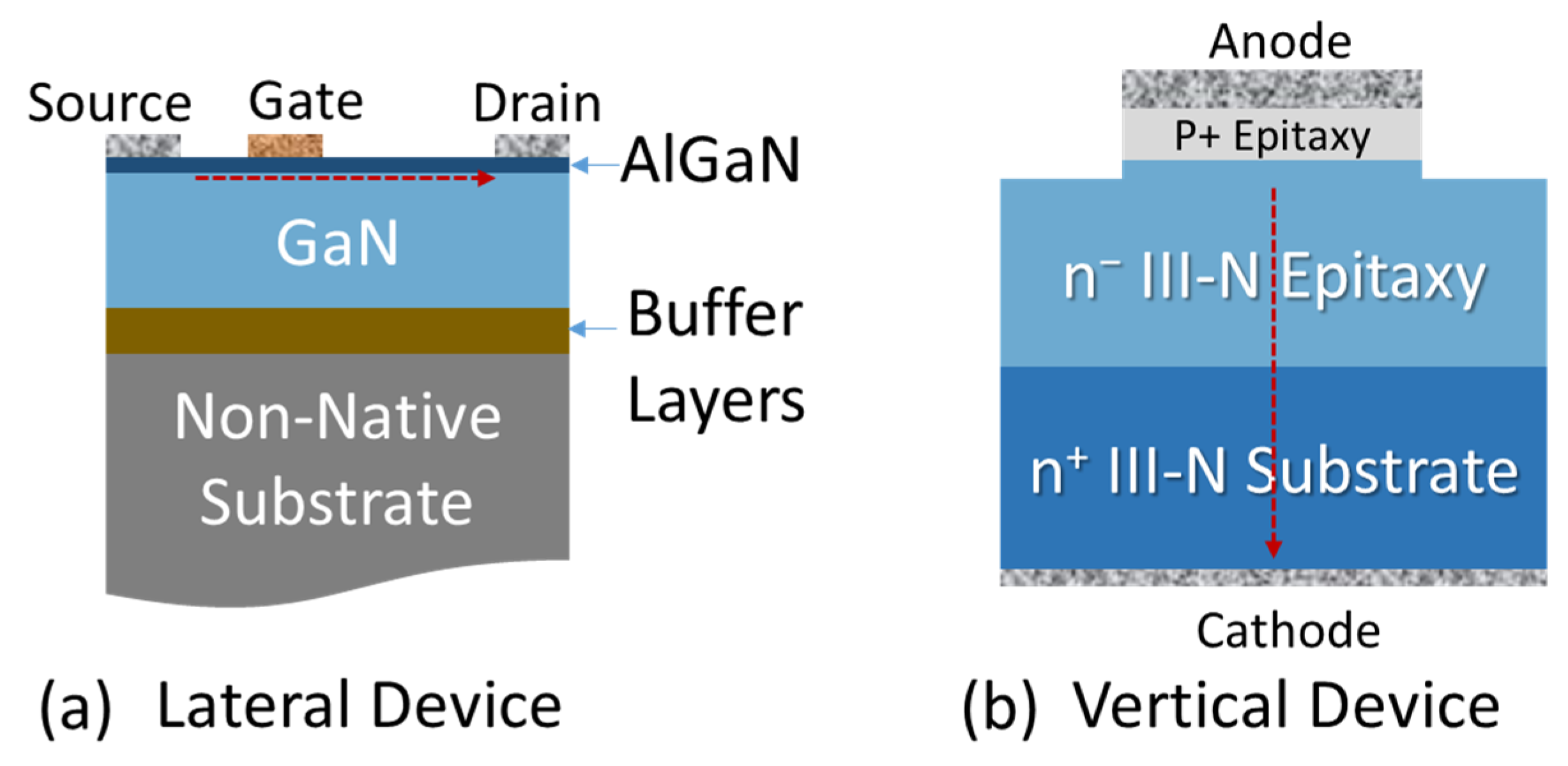
:1. Introduction
2. Understanding Native GaN Substrates
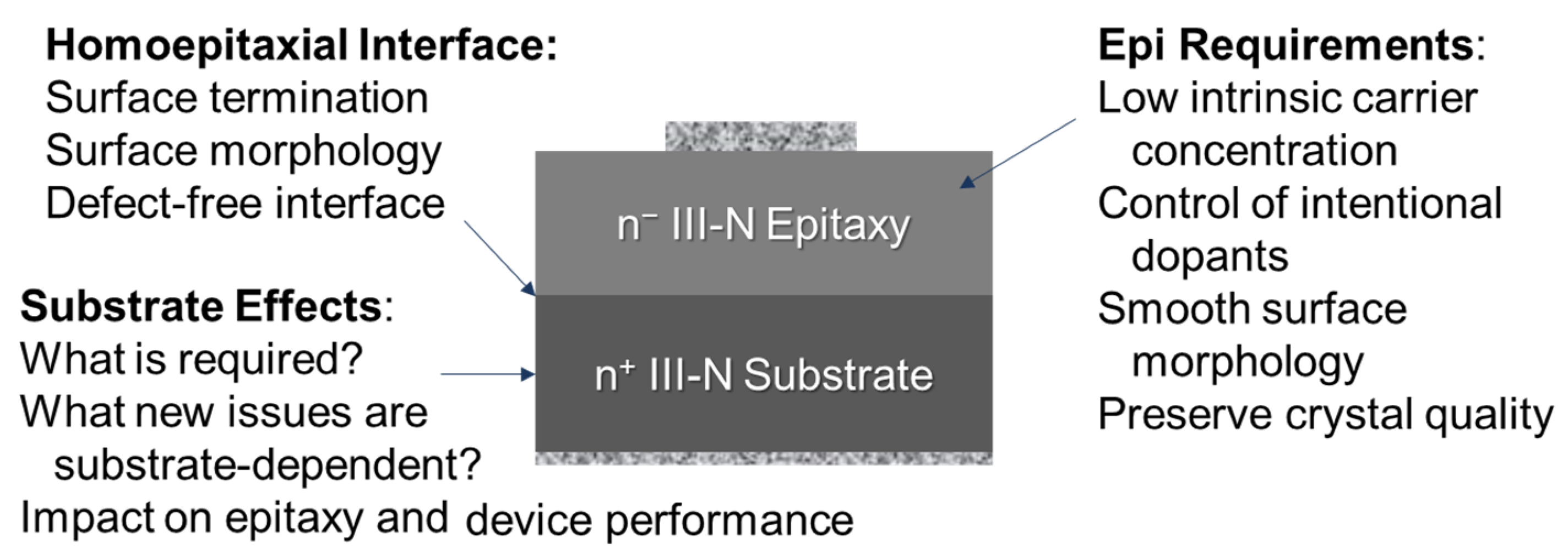
3. Substrate-Epitaxy Effects
4. Homoepitaxial Interface
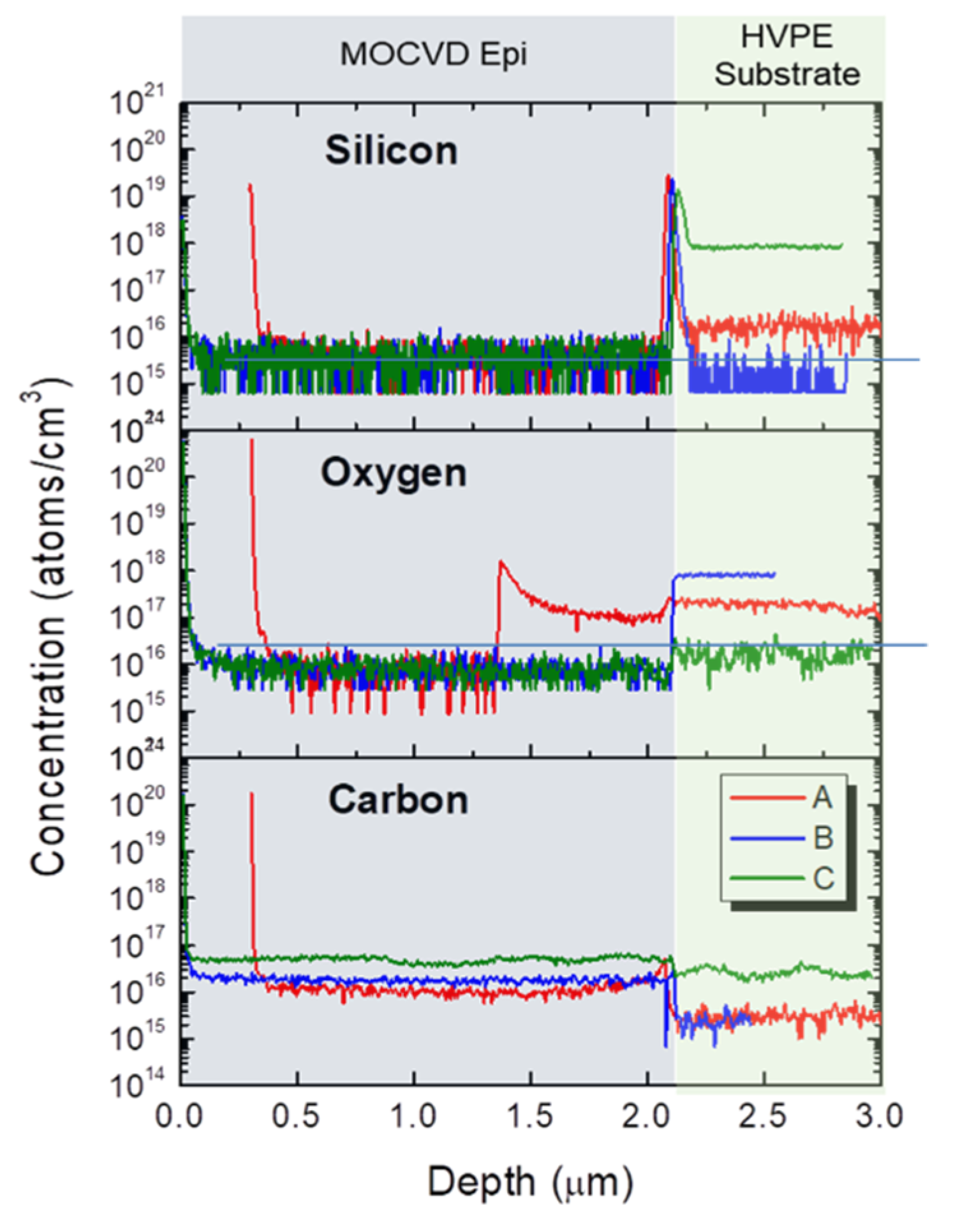
4.1. Composition
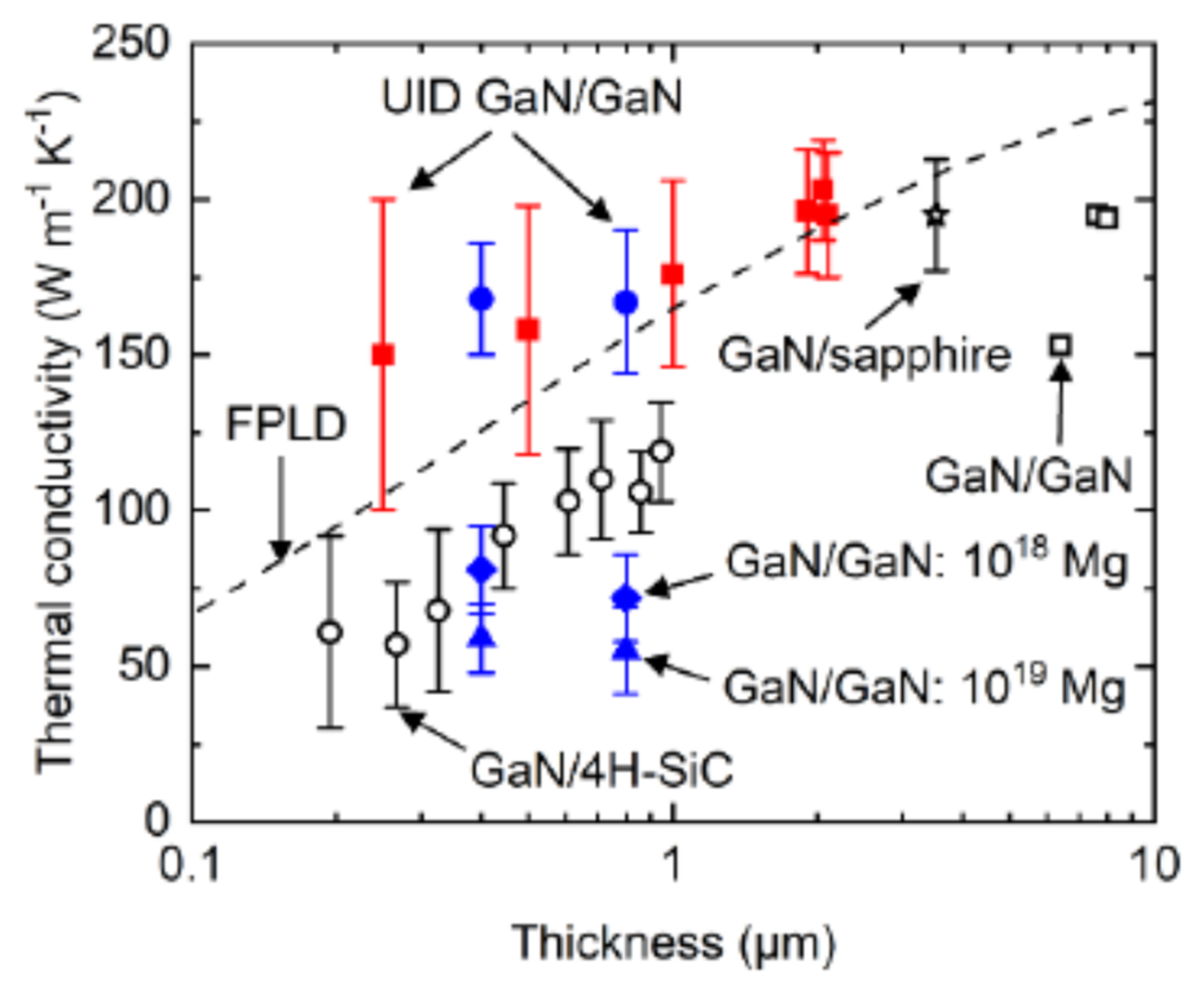
4.2. Thermal Conductivity
5. Impurity Incorporation
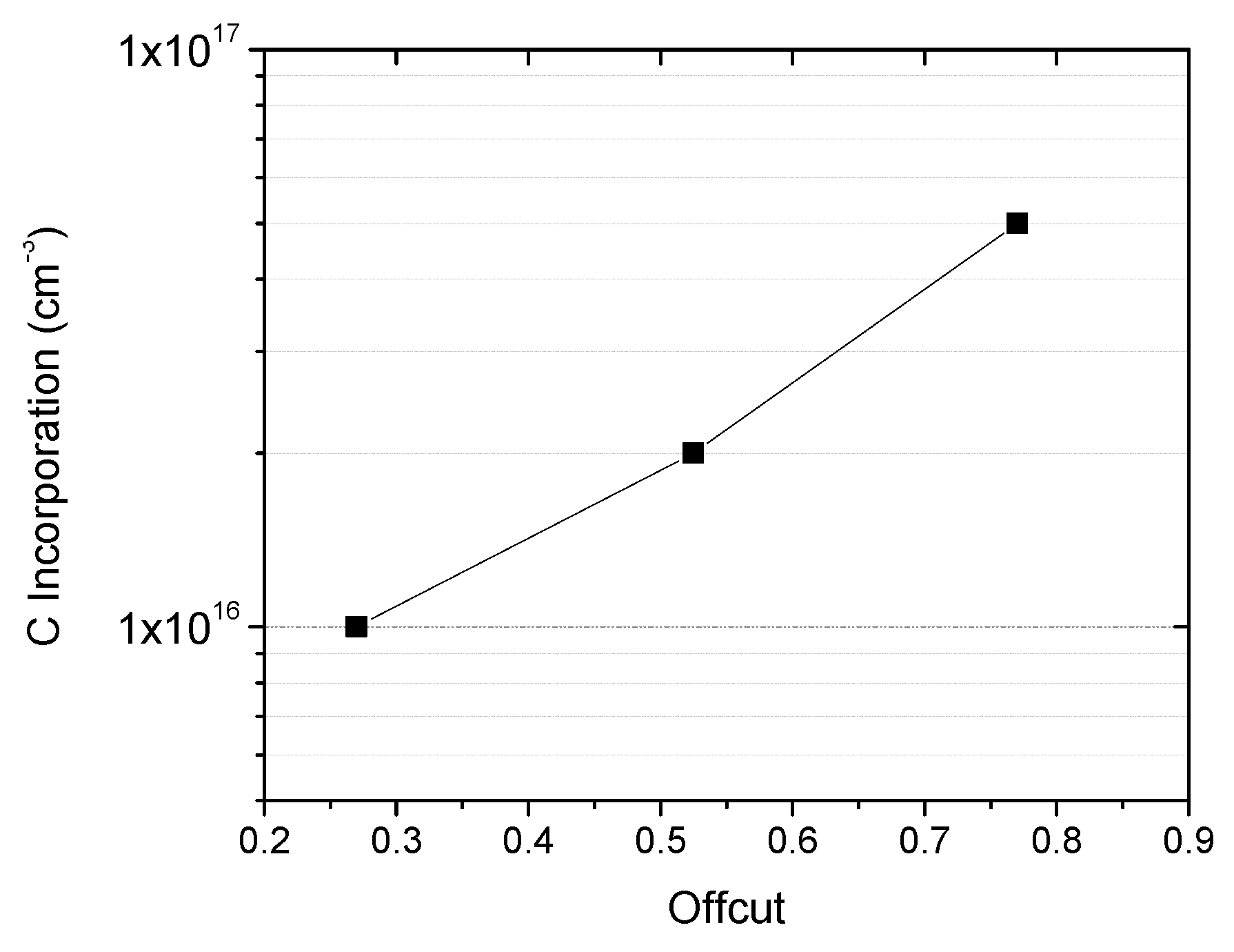
5.1. Carbon in GaN
5.2. Doping in Ultra-Wide Bandgap III-Nitrides
6. Effects on Processing and Device Performance
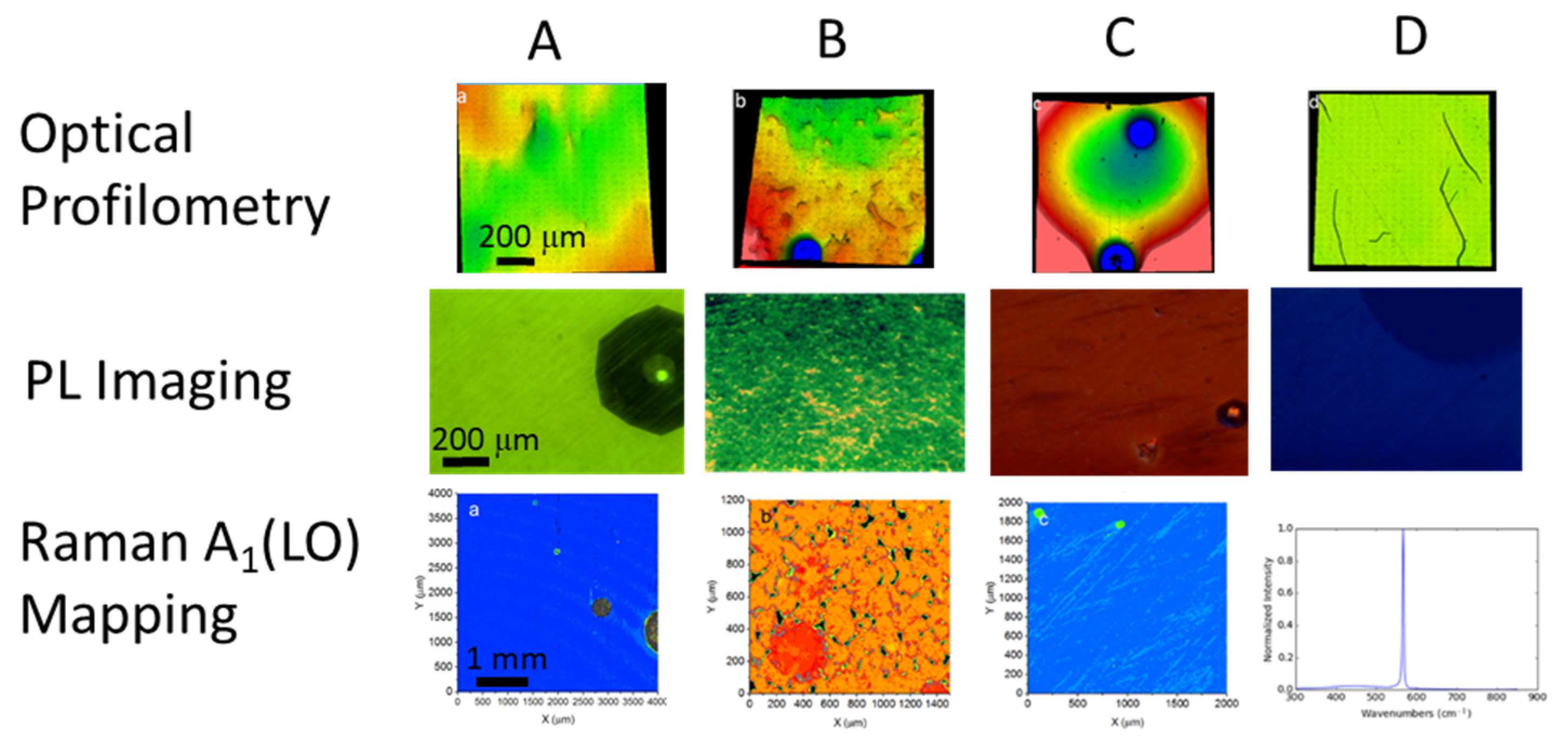
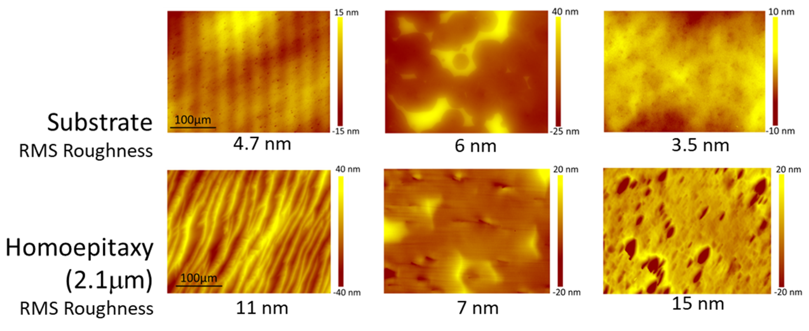
6.1. Surface Roughness
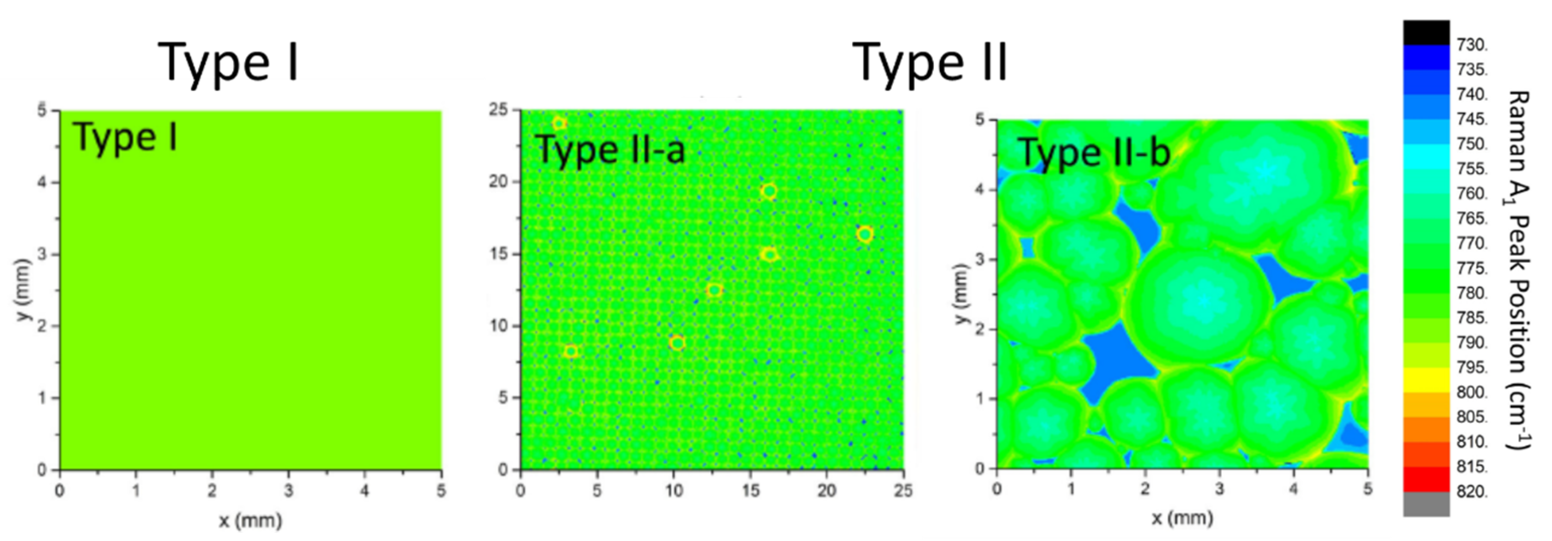
6.2. Inhomogeneity
6.3. Metal-Assisted Chemical (MAC) Etching
7. Summary
Funding
Data Availability Statement
Conflicts of Interest
References
- Nakamura, S. Background Story of the Invention of Efficient InGaN Blue-Light-Emitting Diodes. Angew. Chem. Int. Ed. 2015, 54, 7770–7788. [Google Scholar] [CrossRef]
- Manikandan, M.; Nirmal, D.; Ajayan, J.; Mohankumar, P.; Prajoon, P.; Arivazhagan, L. A review of blue light emitting diodes for future solid state lighting and visible light communication applications. Superlattices Microstruct. 2019, 136, 106294. [Google Scholar] [CrossRef]
- Pengelly, R.S.; Wood, S.M.; Milligan, J.W.; Sheppard, S.T.; Pribble, W.L. A Review of GaN on SiC High Electron-Mobility Power Transistors and MMICs. IEEE Trans. Microw. Theory Technol. 2012, 60, 1764. [Google Scholar] [CrossRef]
- Hamza, K.H.; Nirmal, D. A review of GaN HEMT broadband power amplifiers. Int. J. Electron. Telecommun. 2020, 116, 153040. [Google Scholar] [CrossRef]
- Speck, J.; Rosner, S.J. The role of threading dislocations in the physical properties of GaN and its alloys. Physica B 1999, 24, 273–274. [Google Scholar] [CrossRef]
- Hite, J.; Gaddipati, P.; Meyer, D.; Mastro, M.; Eddy, C. Correlation of threading screw dislocation density to GaN 2-DEG mobility. Electron. Lett. 2014, 50, 1722–1724. [Google Scholar] [CrossRef]
- Termentzidis, K.; Isaiev, M.; Salnikova, A.; Belabbas, I.; Lacrois, D.; Kioseoglu, J. Impact of screw and edge dislocations on the thermal conductivity of individual nanowires and bulk GaN: A molecular dynamics study. Phys. Chem. Chem. Phys. 2018, 20, 5159–5172. [Google Scholar] [CrossRef] [Green Version]
- Meneghini, M.; Tajalli, A.; Moens, P.; Banerjee, A.; Zanoni, E.; Meneghesso, G. Trapping phenomena and degradation mechanisms in GaN-based power HEMTs. Mater. Sci. Semicond. Process. 2018, 78, 118–126. [Google Scholar] [CrossRef]
- Hudgins, J.; Simin, G.; Santi, E.; Khan, M. An assessment of wide bandgap semiconductors for power devices. IEEE Trans. Power Electron. 2003, 18, 907–914. [Google Scholar] [CrossRef] [Green Version]
- Wang, L.-M. Relationship between Intrinsic Breakdown Field and Bandgap of Materials. In Proceedings of the 25th IEEE International Conference on Microelectronics, Belgrade, Serbia and Montenegro, 14–17 May 2006; pp. 576–579. [Google Scholar]
- Utsumi, W.; Saitoh, H.; Kaneko, H.; Watanuki, T.; Aoki, K.; Shimomura, O. Congruent melting of gallium nitride at 6 GPa and its application to single-crystal growth. Nat. Mater. 2003, 2, 735–738. [Google Scholar] [CrossRef]
- Porowski, S.; Sadovyi, B.; Gierlotka, S.; Rzoska, S.; Grzegory, I.; Petrusha, I.; Turkevich, V.; Stratiichuk, D.J. The challenge of decomposition and melting of gallium nitride under high pressure and high temperature. Phys. Chem. Sol. 2015, 85, 138–143. [Google Scholar] [CrossRef] [Green Version]
- Munir, Z.; Searcy, A.J. Activation Energy for the Sublimation of Gallium Nitride. Chem. Phys. 1965, 42, 4223–4428. [Google Scholar] [CrossRef] [Green Version]
- Kucharski, R.; Sochacki, T.; Lucznik, B.; Bockowski, M.J. Growth of bulk GaN crystals. Appl. Phys. 2020, 128, 050902. [Google Scholar] [CrossRef]
- Sochacki, T.; Bryan, Z.; Amilusik, M.; Bobea, M.; Fijalkowski, M.; Bryan, I.; Lucznik, B.; Collazo, R.; Weyher, J.; Kucharsi, R.; et al. HVPE-GaN grown on MOCVD-GaN/sapphire template and ammonothermal GaN seeds: Comparison of structural, optical, and electrical properties. J. Cryst. Growth 2014, 394, 55–60. [Google Scholar] [CrossRef]
- Gallagher, J.; Anderson, T.; Luna, L.; Koehler, A.; Hite, J.; Mahadik, N.; Hobart, K.; Kub, F.J. Long range, non-destructive characterization of GaN substrates for power devices. J. Cryst. Growth 2019, 506, 178–184. [Google Scholar] [CrossRef]
- Kuball, M. Raman spectroscopy of GaN, AlGaN and AlN for process and growth monitoring/control. Surf. Interface Anal. 2001, 31, 987–999. [Google Scholar] [CrossRef]
- Hite, J.; Mastro, M.; Gallagher, J.; Ebrish, M.; Anderson, T.; Freitas, J. GaN Homoepitaxial Growth and Substrate-Dependent Effects for Vertical Power Devices. ECS Trans. 2020, 98, 63–67. [Google Scholar] [CrossRef]
- Gallagher, J.; Anderson, T.; Koehler, A.; Ebrish, M.; Foster, G.; Mastro, M.; Hite, J.; Gunning, B.; Kaplar, R.; Hobart, K.; et al. Optimizing performance and yield of vertical GaN diodes using wafer scale optical techniques. Electr. Mater. 2021, 50, 3013–3021. [Google Scholar] [CrossRef]
- Hite, J.; Anderson, T.; Luna, L.; Gallagher, J.; Mastro, M.; Freitas, J.; Eddy, C., Jr. Influence of HVPE substrates on homoepitaxy of GaN grown by MOCVD. J. Cryst. Growth 2018, 498, 352–356. [Google Scholar] [CrossRef]
- Storm, D.; McConkie, T.; Hardy, M.; Katzer, D.; Nepal, N.; Meyer, D.J. Surface preparation of freestanding GaN substrates for homoepitaxial GaN growth by rf-plasma MBE. Vac. Sci. Technol. B 2017, 35, 02B109. [Google Scholar] [CrossRef]
- Hite, J.; Mastro, M.; Luna, L.; Anderson, T. Understanding Interfaces in Homoepitaxial GaN Growth. ECS Trans. 2018, 86, 15–19. [Google Scholar] [CrossRef]
- Fu, K.; Fu, H.; Liu, H.; Alugubelli, S.; Yang, T.; Huang, X.; Chen, H.; Baranowski, I.; Montes, J.; Ponce, F.; et al. Investigation of GaN-on-GaN vertical p-n diode with regrown p-GaN by metalorganic chemical vapor deposition. Appl. Phys. Lett. 2018, 113, 233502. [Google Scholar] [CrossRef]
- Fu, K.; Fu, H.; Deng, X.; Su, P.; Liu, H.; Hatch, K.; Cheng, C.; Messina, D.; Meidanshahi, R.; Peri, P.; et al. The impact of interfacial Si contamination on GaN-on-GaN regrowth for high power vertical devices. Appl. Phys. Lett. 2021, 118, 222104. [Google Scholar] [CrossRef]
- Noshin, M.; Soman, R.; Xu, X.; Chowdhury, S. A systematic study of the regrown interface impurities in unintentionally doped Ga-polar c-plane GaN and methods to reduce the same. Semicond. Sci. Technol. 2022, 37, 075018. [Google Scholar] [CrossRef]
- Hite, J.; Mastro, M. Chapter 12—Understanding interfaces for homoepitaxial GaN growth. In Wide Bandgap Semiconductor-Based Electronics; Ren, F., Pearton, S., Eds.; IOP Publishing Ltd.: Philadelphia, PA, USA, 2020. [Google Scholar]
- Koh, Y.; Hoque, M.B.; Olson, D.; Ahmad, H.; Liu, Z.; Shi, J.; Steven, W.; Huynh, K.; Hoglund, E.; Howe, J.; et al. High thermal conductivity and thermal boundary conductance of homoepitaxially grown gallium nitride (GaN) thin films. Phys. Rev. Mater. 2021, 5, 104604. [Google Scholar] [CrossRef]
- Hoque, M.B.; Koh, Y.; Aryana, K.; Hoglaund, E.; Braun, J.; Olson, D.; Gaskins, J.; Ahmad, H.; Elahi, M.; Hite, J.; et al. Thermal conductivity measurements of sub-surface buried substrates by steady- state thermoreflectance. Rev. Sci. Instrum. 2021, 92, 064906. [Google Scholar] [CrossRef] [PubMed]
- Lyons, J.; Wickramaratne, D.; Van de Walle, C.J. A first-principles understanding of point defects and impurities in GaN. Appl. Phys. 2021, 129, 111101. [Google Scholar] [CrossRef]
- Armstrong, A.; Arehart, A.; Green, D.; Mishra, U.; Speck, J.; Ringel, S.J. Impact of deep levels on the electrical conductivity and luminescence of gallium nitride codoped with carbon and silicon. Appl. Phys. 2005, 98, 053704. [Google Scholar] [CrossRef]
- Bakhtiary-Noodeh, M.; Detchprohm, T.; Dupuis, R.D. Carbon and silicon background impurity control in undoped GaN layers grown with trimethylgallium and triethylgallium via metalorganic chemical vapor deposition. J. Cryst. Growth 2023, 602, 126982. [Google Scholar] [CrossRef]
- Li, X.; Danielsson, O.; Pedersen, H.; Janzen, E.; Forsberg, U.J. Precursors for carbon doping of GaN in chemical vapor deposition. Vac. Sci. Technol. B 2015, 33, 021208. [Google Scholar] [CrossRef] [Green Version]
- Erwin, S.C.; Lyons, J.L. Atomic Layer Epitaxy of Aluminum Nitride: Unraveling the Connection between Hydrogen Plasma and Carbon Contamination. ACS Appl. Mater. Interfaces 2018, 10, 20142. [Google Scholar] [CrossRef] [PubMed]
- Lyons, J.; Glaser, E.; Zvanut, M.; Paudel, S.; Iwinska, M.; Sochacki, T.; Bockowski, M. Carbon complexes in highly C-doped GaN. Phys. Rev. B 2021, 104, 075201. [Google Scholar] [CrossRef]
- Lyons, J.; Janotti, A.; Van de Walle, C. Carbon impurities and the yellow luminescence in GaN. Appl. Phys. Lett. 2010, 97, 152108. [Google Scholar] [CrossRef]
- Walukiewicz, W. Intrinsic limitations to the doping of wide-gap semiconductors. Physica B 2001, 302–303, 123–134. [Google Scholar] [CrossRef]
- Lyons, J.; Van de Walle, C. Hole trapping at acceptor impurities and alloying elements in AlN. Phys. Status Sol. RRL 2021, 15, 2100218. [Google Scholar] [CrossRef]
- Taniyasu, Y.; Kasu, M.; Makimoto, T. An aluminium nitride light-emitting diode with a wavelength of 210 nanometres. Nature 2006, 441, 325–328. [Google Scholar] [CrossRef] [PubMed]
- Wu, R.; Shen, L.; Yang, M.; Sha, Z.; Cai, Y.; Feng, Y. Possible efficient p-type doping of AlN using Be: An ab initio study. Appl. Phys. Lett. 2007, 91, 152110. [Google Scholar] [CrossRef]
- Ahmad, H.; Lindemuth, J.; Engel, Z.; Matthews, C.; McCrone, T.; Doolittle, W. Substantial P-Type Conductivity of AlN Achieved via Beryllium Doping. Adv. Mater. 2021, 33, 2104497. [Google Scholar] [CrossRef] [PubMed]
- Turiansky, M.; Wickramaratne, D.; Lyons, J.; Van de Walle, C. Prospects for n-type conductivity in cubic boron nitride. Appl. Phys. Lett. 2021, 119, 162105. [Google Scholar] [CrossRef]
- Hite, J.; Anderson, T.; Mastro, M.; Luna, L.; Gallagher, J.; Myers-Ward, R.; Hobart, K.; Eddy, C., Jr. Effect of Surface Morphology on Diode Performance in Vertical GaN Schottky Diodes. ECS J. Sol. State Sci. Technol. 2017, 6, S3103–S3105. [Google Scholar] [CrossRef] [Green Version]
- Kizilyalli, I.; Bui-Quang, P.; Disney, D.; Bhatia, H.; Aktas, O. Reliability studies of vertical GaN devices based on bulk GaN substrates. Microelectron. Reliab. 2015, 55, 1645–1661. [Google Scholar] [CrossRef]
- Chan, C.; Shuyumi, N.; Hite, J.; Mastro, M.; Qadri, S.; Li, X. Homoepitaxial GaN micropillar array by plasma-free photo-enhanced metal-assisted chemical etching. J. Vac. Sci. Technol. A 2021, 39, 053212. [Google Scholar] [CrossRef]
Disclaimer/Publisher’s Note: The statements, opinions and data contained in all publications are solely those of the individual author(s) and contributor(s) and not of MDPI and/or the editor(s). MDPI and/or the editor(s) disclaim responsibility for any injury to people or property resulting from any ideas, methods, instructions or products referred to in the content. |
© 2023 by the author. Licensee MDPI, Basel, Switzerland. This article is an open access article distributed under the terms and conditions of the Creative Commons Attribution (CC BY) license (https://creativecommons.org/licenses/by/4.0/).
Share and Cite
Hite, J.K. A Review of Homoepitaxy of III-Nitride Semiconductors by Metal Organic Chemical Vapor Deposition and the Effects on Vertical Devices. Crystals 2023, 13, 387. https://doi.org/10.3390/cryst13030387
Hite JK. A Review of Homoepitaxy of III-Nitride Semiconductors by Metal Organic Chemical Vapor Deposition and the Effects on Vertical Devices. Crystals. 2023; 13(3):387. https://doi.org/10.3390/cryst13030387
Chicago/Turabian StyleHite, Jennifer K. 2023. "A Review of Homoepitaxy of III-Nitride Semiconductors by Metal Organic Chemical Vapor Deposition and the Effects on Vertical Devices" Crystals 13, no. 3: 387. https://doi.org/10.3390/cryst13030387